

Page 1
OPEN/
CLOSE
0
Î
¡
1
¢
STANDBY/ON
4
DV-454-K
3
8
7
DVD PLAYER
DV-454-K
DV-454-S
THIS MANUAL IS APPLICABLE TO THE FOLLOWING MODEL(S) AND TYPE(S).
Model Power Requirement
DV-454-K AC220-240V 2
DV-454-K AC220-240V 2
DV-454-K AC220-240V 2
DV-454-S
DV-454-S
DV-454-S
WYXU
WYXU/FRGR
WVXU
WYXU
WYXU/FRGR
WVXU
Type
AC220-240V 2
AC220-240V
AC220-240V
Regional restriction
codes (Region No.)
2
2
ORDER NO.
RRV2610
Remarks
Confirm it
Serial No.
For details, refer to "Important symbols for good services".
PIONEER CORPORATION 4-1, Meguro 1-chome, Meguro-ku, Tokyo 153-8654, Japan
PIONEER ELECTRONICS (USA) INC. P.O. Box 1760, Long Beach, CA 90801-1760, U.S.A.
PIONEER EUROPE NV Haven 1087, Keetberglaan 1, 9120 Melsele, Belgium
PIONEER ELECTRONICS ASIACENTRE PTE. LTD. 253 Alexandra Road, #04-01, Singapore 159936
PIONEER CORPORATION 2002
T – ZZE MAY 2002 Printed in Japan
Page 2
1
SAFETY INFORMATION
A
This service manual is intended for qualified service technicians ; it is not meant for the casual doit-yourselfer. Qualified technicians have the necessary test equipment and tools, and have been
trainedto properly and safely repair complex products such as those covered by this
manual.Improperly performed repairs can adversely affect the safety and reliability of the product
and mayvoid the warranty. If you are not qualified to perform the repair of this product properly and
safely, youshould not risk trying to do so and refer the repair to a qualified service technician.
23
4
B
C
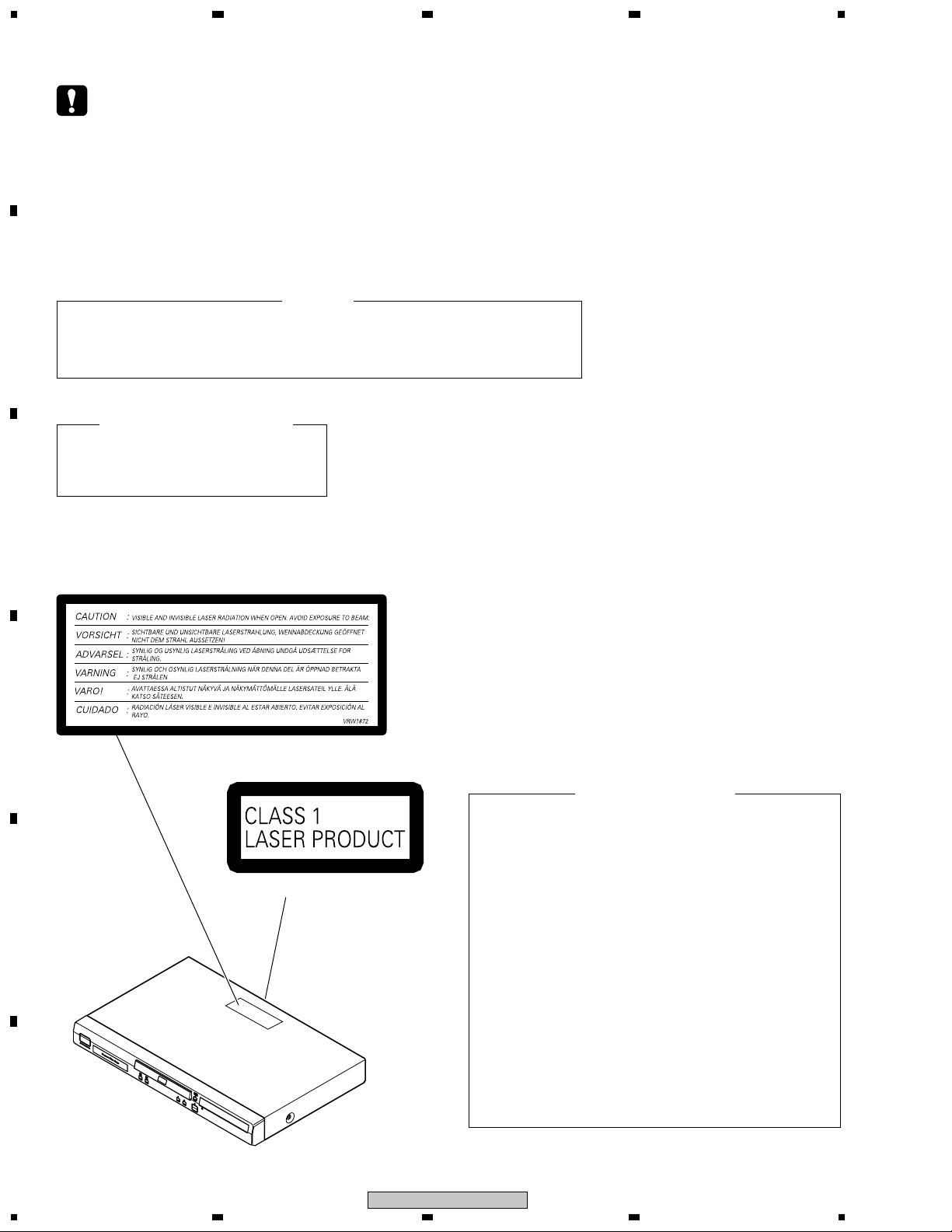
THE AEL (ACCESSIBLE EMISSION LEVEL) OF THE LASER POWER OUTPUT IS LESS THAN CLASS 1
BUT THE LASER COMPONENT IS CAPABLE OF EMITTING RADIATION EXCEEDING THE LIMIT FOR
CLASS 1.
A SPECIALLY INSTRUCTED PERSON SHOULD DO SERVICING OPERATION OF THE APPARATUS.
LASER DIODE CHARACTERISTICS
FOR DVD : MAXIMUM OUTPUT POWER : 5 mW
WAVELENGTH : 650 nm
FOR CD : MAXIMUM OUTPUT POWER : 5 mW
WAVELENGTH : 780 nm
WARNING !
LABEL CHECK
D
Additional Laser Caution
1. Laser Interlock Mechanism
• Loading switch (S101 on the LOAB Assy) is used for interlock
mechanism of the laser.
When this switch turned ON in SW2 (XCLOSE) side (OPEN signal is
0V and XCLOSE signal is 3.5V), a laser becomes the status which can
(Printed on the Rear Panel)
E
F
2
1234
DV-454-K
completely oscillation.
Furthermore, the laser completely oscillates in the disc judgment and
disc playback.
When player is power ON state and laser diode is not completely
oscillating, 780nm laser diode is always oscillating by half power.
• Laser diode is driving with Q101 (650nm LD) and Q102 (780nm LD)
on the FJMB Assy.
Therefore, when short-circuit between the emitter and collector of these
transistors or the base voltage is supplied for transistors turn on, the
laser oscillates. (failure mode)
• In the test mode ∗ , there is the mode that the laser oscillates except
for the disc judgment and playback. LD ON mode in the test mode
oscillates with the laser forcibly.
The interlock mechanism mentioned above becomes invalid in this
mode.
2. When the cover is open, close viewing through the objective lens with
the naked eye will cause exposure to the laser beam.
∗ : See page 53.
Page 3
5
678
[ Important symbols for good services ]
In this manual, the symbols shown-below indicate that adjustments, settings or cleaning should be made securely.
When you find the procedures bearing any of the symbols, be sure to fulfill them:
1. Product safety
You should conform to the regulations governing the product (safety, radio and noise, and other regulations), and
should keep the safety during servicing by following the safety instructions described in this manual.
2. Adjustments
To keep the original performances of the product, optimum adjustments or specification confirmation is indispensable.
In accordance with the procedures or instructions described in this manual, adjustments should be performed.
3. Cleaning
For optical pickups, tape-deck heads, lenses and mirrors used in projection monitors, and other parts requiring cleaning,
proper cleaning should be performed to restore their performances.
4. Shipping mode and shipping screws
To protect the product from damages or failures that may be caused during transit, the shipping mode should be set or
the shipping screws should be installed before shipping out in accordance with this manual, if necessary.
5. Lubricants, glues, and replacement parts
Appropriately applying grease or glue can maintain the product performances. But improper lubrication or applying
glue may lead to failures or troubles in the product. By following the instructions in this manual, be sure to apply the
prescribed grease or glue to proper portions by the appropriate amount.For replacement parts or tools, the prescribed
ones should be used.
A
B
C
Discs compatible with this
player
Any disc that displays one of the following
logos should play in this player. Other
formats, including DVD-Audio, DVD-RAM,
DVD-ROM, CD-ROM (except those that
contain MP3 files), SACD and Photo CD will
not play.
DVD-Video
Audio-CD
Video-CD CD-R CD-RW
D
E
F
DV-454-K
5
6
7
8
3
Page 4

CONTENTS
A
1
23
1. SPECIFICATIONS .................................................................................................................................................5
2. EXPLODED VIEWS AND PARTS LIST ............................................................................................................... 6
2.1 PACKING ........................................................................................................................................................ 6
2.2 EXTERIOR SECTION ..................................................................................................................................... 8
2.3 LOADING MECHANISM ASSY ................................................................................................................... 10
2.4 TRAVERSE MECHANISM ASSY-S ............................................................................................................ 14
3. BLOCK DIAGRAM AND SCHEMATIC DIAGRAM ............................................................................................ 16
3.1 BLOCK DIAGRAM ....................................................................................................................................... 16
3.1.1 SIGNAL ROUTE ........................................................................................................................................ 16
B
3.1.2 POWER SUPPLY BLOCK ........................................................................................................................ 18
3.1.3 WAVEFORMS ........................................................................................................................................... 19
3.2 LOAB ASSY and OVERALL WIRING DIAGRAM ........................................................................................20
3.3 FJMB ASSY 1/5 [FRONT END BLOCK] ...................................................................................................... 22
3.4 FJMB ASSY 2/5 [BACK END BLOCK] ........................................................................................................ 24
3.5 FJMB ASSY 3/5 [AUDIO BLOCK] ............................................................................................................... 26
3.6 FJMB ASSY 4/5 [VIDEO BLOCK] ................................................................................................................ 28
3.7 FJMB ASSY 5/5 [FL CONTROL BLOCK] .................................................................................................... 30
3.8 IRKY and PSWB ASSYS ............................................................................................................................. 32
3.9 POWER SUPPLY UNIT (VWR1352) ........................................................................................................... 34
C
3.10 POWER SUPPLY UNIT (VWR1354) ......................................................................................................... 35
3.11 SCRB ASSY ............................................................................................................................................... 36
4. PCB CONNECTION DIAGRAM ......................................................................................................................... 39
4.1 LOAB ASSY ................................................................................................................................................. 39
4.2 FJMB ASSY.................................................................................................................................................. 40
4.3 IRKY and PSWB ASSYS ............................................................................................................................. 44
4.4 POWER SUPPLY UNIT (VWR1352) ........................................................................................................... 45
4.5 POWER SUPPLY UNIT (VWR1354) ........................................................................................................... 46
4.6 SCRB ASSY ................................................................................................................................................. 47
5. PCB PARTS LIST ............................................................................................................................................... 48
D
6. ADJUSTMENT .................................................................................................................................................... 51
6.1 ADJUSTMENT ITEMS AND LOCATION ..................................................................................................... 51
6.2 JIGS AND MEASURING INSTRUMENTS ................................................................................................... 51
6.3 NECESSARY ADJUSTMENT POINTS ....................................................................................................... 52
6.4 TEST MODE ................................................................................................................................................. 53
6.5 MECHANISM ADJUSTMENT ...................................................................................................................... 54
7. GENERAL INFORMATION ................................................................................................................................ 57
7.1 DIAGNOSIS.................................................................................................................................................. 57
7.1.1 TEST MODE.............................................................................................................................................. 57
E
7.1.2 DISPLAY OF THE MECHANISM ERROR HISTORY .............................................................................. 63
7.1.3 TEST POINTS LOCATION & WAVEFORMS ........................................................................................... 66
7.1.4 TROUBLE SHOOTING ............................................................................................................................. 71
7.1.5 SEQUENCE AFTER THE POWER ON .................................................................................................... 73
7.1.6 DISASSEMBLY ......................................................................................................................................... 74
7.2 IC .................................................................................................................................................................. 79
7.3 CLEANING ................................................................................................................................................... 97
8. PANEL FACILITIES ............................................................................................................................................ 98
4
F
4
1234
DV-454-K
Page 5
5
1. SPECIFICATIONS
678
General
System ........................... DVD-Video, Video CD
CD and MP3 files
Power requirements.... AC 220–240 V, 50/60 Hz
Power consumption..................................14 W
Power consumption (standby)
Weight .................................................... 2.5 kg
Dimensions
DV-454 ............ 420 (W) x 55 (H) x 278 (D) mm
Operating temperature..............+5°C to +35°C
Operating humidity .........................5% to 85%
S-Video output
Y (luminance) - Output level..........1 Vp-p (75 Ω)
C (color) - Output level.......... 286 mVp-p (75 Ω)
Jack .............................................. S-Video jack
Video output
Output level ..................................1 Vp-p (75 Ω)
Jack ...................................................RCA jack
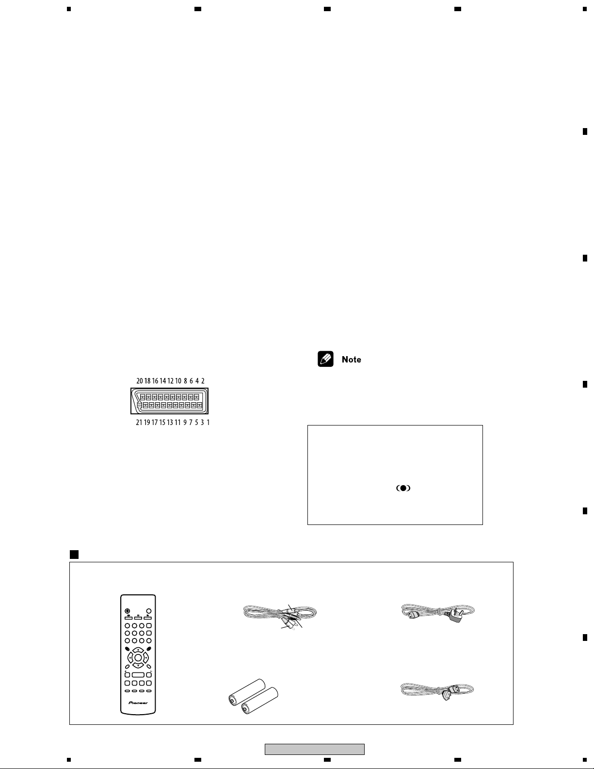
AV connector output
AV Connectors (21-pin connector assignment)
AV connector input/output ..... 21-pin connector
This connector provides the video and audio
signals for connection to a compatible colour
TV or monitor.
..................... 0.3 W
(no condensation)
Audio output (1 stereo pair)
Output level .......................During audio output
200 mVrms (1 kHz, –20 dB)
Number of channels ...................................... 2
Jacks ................................................. RCA jack
Digital audio characteristics
Frequency response................... 4 Hz to 44 kHz
(DVD fs: 96 kHz)
S/N ratio ................................................118 dB
Dynamic range ...................................... 101 dB
Total harmonic distortion .....................0.0016 %
Wow and flutter..............Limit of measurement
(0.001% W. PEAK) or lower
Digital output
Optical digital output ...........Optical digital jack
Coaxial digital output ......................... RCA jack
Accessories
Audio/video cable ...........................................1
Power cable.................................................. . 1
Remote control............................................... 1
AA/R6P dry cell batteries ............................... 2
Operating Instructions ....................................1
Warranty card .................................................1
• The specifications and design of this
product are subject to change without
notice, due to improvement.
A
B
C
PIN no.
1 ........................................................... Audio 2/R out
3 ........................................................... Audio 1/L out
4 ..........................................................................GND
7 .........................................................................B out
8 .......................................................................Status
11 ....................................................................... G out
15 ................................................................R or C out
17 ........................................................................GND
19 ................................................... Video out or Y out
21 ........................................................................GND
Accessories
Remote Control : VXX2800
OPEN/CLOSE
STANDBY/ON
0
ANGLEAUDIO
SUBTITLE
CLEAR
23
1
ENTER
56
4
0
789
TOP MENU
MENU
ENTER
SETUP
RETURN
E/
/e
13
¡
8
4
7
¢
PLAY MODE SURROUND ZOOM DISPLAY
Audio/Video Cable (L=1.5m): XDE3049
Yellow
AA/R6P Dry Cell Batteries
White
• Manufactured under license from Dolby
Laboratories. “Dolby” and the double-D
symbol are trademarks of Dolby Laboratories.
• “DTS” is a registered trademark of Digital
Theater Systems, Inc.
• TruSurround and the
® symbol are
trademarks of SRS Labs, Inc. TruSurround
technology is incorporated under license from
SRS Labs, Inc.
Power Cable [WVXU Type]
: ADG1156
Red
Power Cable [Other Types]
: ADG1154
D
E
F
DV-454-K
5
6
7
8
5
Page 6
1
23
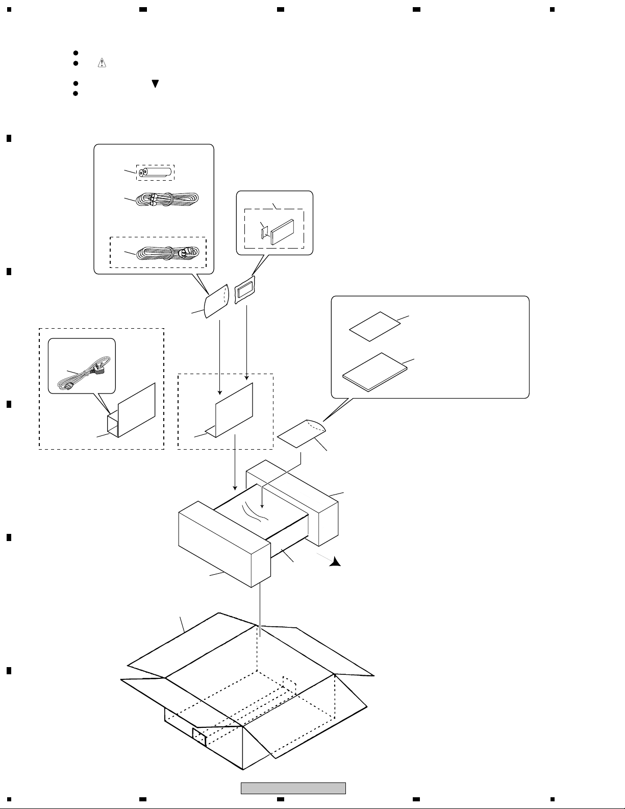
2. EXPLODED VIEWS AND PARTS LIST
NOTES:
A
2.1 PACKING
Parts marked by "NSP" are generally unavailable because they are not in our Master Spare Parts List.
The mark found on some component parts indicates the importance of the safety factor of the part.
Therefore, when replacing, be sure to use parts of identical designation.
Screws adjacent to mark on product are used for disassembly.
For the applying amount of lubricants or glue, follow the instructions in this manual.
(In the case of no amount instructions, apply as you think it appropriate.)
3
4
B
WVXU Type Only
C
1
17
D
8
WYXU and WYXU/FRGR
Types Only
1
4
11
7
14
WYXU
and WYXU/FRGR
Types Only
2
5, 6, 15, 16
"Operating Instructions"
4
10
13
9
FRONT
E
F
6
1234
12
DV-454-K
Page 7
5
(2) CONTRAST TABLE
Mark No. RemarksSymbol and Description
Part No.
DV-454-K DV-454-S
WYXU
WYXU/FRGR
WVXU WYXU
WYXU/FRGR
WVXU
> 1
5
6
11
12
15
16
17
Power Cable
Operating Instructions (English / Italian)
Operating Instructions (French / German)
Paper Board
Packing Case
Operating Instructions (Spanish / Dutch)
Operating Instructions (English)
Accessory Box
ADG1154
VRD1151
VRD1152
VHC1089
VHG2185
VRD1153
Not used
Not used
ADG1154
Not used
VRD1152
VHC1089
VHG2201
Not used
Not used
Not used
ADG1156
Not used
Not used
Not used
VHG2181
Not used
VRB1286
VHC1092
ADG1154
VRD1151
VRD1152
VHC1089
VHG2182
VRD1153
Not used
Not used
ADG1154
Not used
VRD1152
VHC1089
VHG2203
Not used
Not used
Not used
ADG1156
Not used
Not used
Not used
VHG2202
Not used
VRB1286
VHC1092
DV-454-K/WYXU, WYXU/FRGR, WVXU, DV-454-S/WYXU, WYXU/FRGR and WVXU are constructed the same except for the
following :
678
(1) PACKING PARTS LIST
Mark No. Description Part No.
> 1 Power Cable See Contrast table (2)
NSP 2 Warranty Card ARY7022
NSP 3 AA/R6P Dry Cell Battery VEM1030
4 Polyethylene Bag VHL1051
5 Operating Instructions See Contrast table (2)
(English / Italian)
6 Operating Instructions See Contrast table (2)
(French / German)
7 Remote Control VXX2800
8 Audio/Video Cable (L=1.5m) XDE3049
9 Pad L VHA1297
10 Pad R VHA1298
11 Paper Board See Contrast table (2)
12 Packing Case See Contrast table (2)
13 Seat Z23-007
14 Battery Cover VNK4997
15 Operating Instructions See Contrast table (2)
(Spanish / Dutch)
A
B
16 Operating Instructions See Contrast table (2)
(English)
17 Accessory Box See Contrast table (2)
C
D
E
5
6
DV-454-K
7
F
7
8
Page 8
1
2.2 EXTERIOR SECTION
23
4
A
25
Refer to
"2.3 LOADING MECHANISM ASSY".
B
C
NON-CONTACT
SIDE
CONTACT
SIDE
8
22
7
23
E
26
11
22
10
23
F
E
D
C
13
G
28
22
22
22
G
B
5
22
27
22
F
B
E
D
C
23
32
23
25
23
23
23
G
22
14
24
18
24
12
24
24
C
24
24
16
24
17
24
24
A
1
4
29
D
24
19
2
D
E
F
29
20
15
16
30
31
6
A
9
B
3
8
1234
DV-454-K
Page 9
5
(2) CONTRAST TABLE
Mark No. RemarksSymbol and Description
Part No.
DV-454-K DV-454-S
WYXU
WYXU/FRGR
WVXU WYXU
WYXU/FRGR
WVXU
13
18
19
20
25
26
30
31
Rear Panel
Tray Panel Assy
Front Panel Assy
Pioneer Badge
Screw
Bonnet Case S
Tray Panel
Sub Panel
VNA2441
VXA2514
VXA2497
VAM1130
BCZ40P060FZK
VXX2831
VNK4976
VNK5043
VNA2439
VXA2506
VXA2498
VAM1129
BCZ40P060FNI
VXX2823
VNK4979
VNK4977
DV-454-K/WYXU, WYXU/FRGR, WVXU, DV-454-S/WYXU, WYXU/FRGR and WVXU are constructed the same except for the
following :
(1) EXTERIOR PARTS LIST
678
Mark No. Description Part No.
NSP 1 IRKY Assy VWG2344
NSP 2 PWSB Assy VWG2345
3 FJMB Assy VWS1518
4 Connector Assy PF05PP-Q12
5 Connector Assy PF13PP-D25
6 Connector Assy PG05KK-E37
> 7 POWER SUPPLY Unit VWR1354
(or VWR1352)
NSP 8 Loading Mechanism Assy VWT1197
9 Leg Assy SX AEC7113
10 Cord Clamper RNH-184
11 Pcb Support VEC2184
NSP 12 Base Chassis VNA2410
13 Rear Panel See Contrast table (2)
14 PCB Base VNE2278
15 DVD V Plate VAM1120
16 Rubber Foot VEB1325
17 FP Angle VNE2270
18 Tray Panel Assy See Contrast table (2)
19 Front Panel Assy See Contrast table (2)
20 Pioneer Badge See Contrast table (2)
21 ••••••
22 Screw BBZ30P060FMC
23 Screw BBZ30P080FZK
24 Screw BBZ30P100FZK
25 Screw See Contrast table (2)
A
B
C
26 Bonnet Case S See Contrast table (2)
27 SCRB Assy VWV1903
28 Flexible Cable (20P) VDA1892
29 Ring VNK4982
30 Tray Panel See Contrast table (2)
31 Sub Panel See Contrast table (2)
32 Label VRW1872
D
E
F
5
6
DV-454-K
7
9
8
Page 10
1
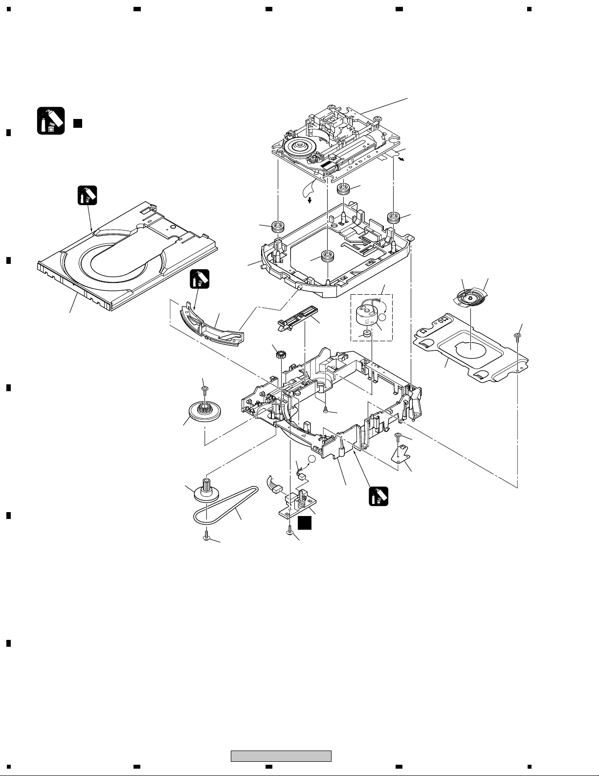
2.3 LOADING MECHANISM ASSY
A
23
4
Note :
Refer to
" Application of Lubricant".
B
C
23
Daifree
GEM1036
Lubricating Oil
GYA1001
13
22
12
To FJMB
CN251
8
8
17
16
8
A
4
2
Refer to
"2.4 TRAVERSE MECHANISM
ASSY-S".
6
To FJMB
CN151
8
3
5
18
19
20
22
21
15
22
D
14
9
22 22
E
7
A
10
A
11
1
Lubricating Oil
GYA1001
F
10
1234
DV-454-K
Page 11

5
LOADING MECHANISM ASSY PARTS LIST
•
678
Mark No. Description Part No.
NSP 1 LOAB Assy VWG2279
2 Traverse Mechanism Assy-S VXX2782
3 Loading Motor Assy VXX2505
4 Motor Pulley PNW1634
5 Carriage DC Motor / 0.3W PXM1027
6 Flexible Cable (26P) VDA1865
7 Connector Assy 2P VKP2253
8 Float Rubber VEB1327
9 Belt VEB1330
10 Stabilizer VNE2253
11 Loading Base VNL1917
12 Float Base DVD VNL1918
13 Drive Cam VNL1919
14 Gear Pulley VNL1921
15 Loading Gear VNL1922
16 Drive Gear VNL1923
17 SW Lever VNL1925
18 Clamper Plate VNE2251
19 Bridge VNE2252
20 Clamper VNL1924
A
B
C
21 Screw JGZ17P028FMC
22 Screw Z39-019
23 Tray VNL1920
D
E
F
DV-454-K
5
6
7
8
11
Page 12
1
23
4
Application of Lubricant
A
Lubricating Oil
GYA1001
Around the shaft
No. 11
Loading Base
B
Lubricating Oil
GYA1001
Lubricating Oil
No. 13
Drive Cam
Lubricating Oil
GYA1001
GYA1001
C
No. 13
Rear View
Inner side of a ditch
Lubricating Oil
GYA1001
D
No. 23
Tray
E
Inner side of a ditch
Lubricating Oil
GYA1001
Daifree
GEM1036
Concave of unevenness
Top View
No. 23
Tray
Inner side of a ditch
Drive Cam
Daifree
GEM1036
Concave of unevenness
Daifree
GEM1036
Top View
Concave of unevenness
Daifree
GEM1036
F
12
1234
DV-454-K
Bottom View
Side of the rib
Daifree
GEM1036
Page 13

5
678
A
B
C
D
E
F
DV-454-K
5
6
7
8
13
Page 14
1
23
2.4 TRAVERSE MECHANISM ASSY-S
A
18
17 (Torque : 0.12 ± 0.01 N•m)
Silicone Adhesive
12
8
GEM1037
3
4
10
18
B
1
13
C
D
16
18
10
7
14
6
19
4 (Adjustment Screw)
5
Screw Tight
5
GYL1001
17 (Torque : 0.12 ± 0.01 N•m)
17
(Torque : 0.12 ± 0.01 N•m)
15
Silicone Adhesive
GEM1037
9
Silicone Adhesive
GEM1037
16
2
NON-CONTACT
E
11
F
14
1234
DV-454-K
SIDE
CONTACT SIDE
Page 15

5
TRAVERSE MECHANISM ASSY-S PARTS LIST
•
678
Mark No. Description Part No.
1 Spindle Motor VXM1088
(or VXM1089)
2 Stepping Motor VXM1090
(or VXM1091)
3 Pickup Assy-S OXX8003
4 Skew Screw VBA1080
5 Skew Spring VBH1335
6 Guide Bar VLL1514
7 Sub Guide Bar VLL1515
8 Hold Spring VNC1017
9 Joint Spring VNC1019
10 Support Spring VNC1020
NSP 11 Mechanism Chassis VNE2248
12 Slider VNL1811
13 Spacer VNL1913
14 Joint VNL1914
15 FFC Holder VNL1915
A
B
16 Screw BBZ20P050FZK
17 Tapping Screw OBA8009
18 Screw PMA26P100FMC
19 Damper Sheet VEB1335
C
D
E
F
DV-454-K
5
6
7
8
15
Page 16
1
23
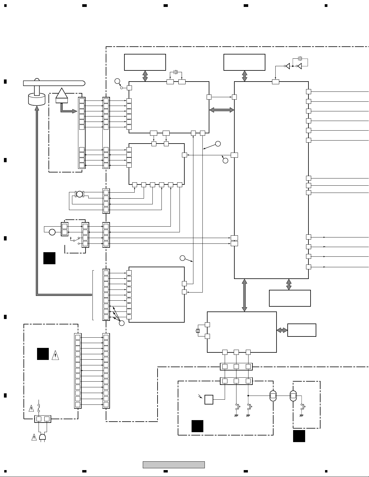
3. BLOCK DIAGRAM AND SCHEMATIC DIAGRAM
3.1 BLOCK DIAGRAM
A
3.1.1 SIGNAL ROUTE
Spindle
Motor
B
PICKUP
C
Loading
Motor
Assy
M
A
D
VWR1352: CN101
VWR1354: CN2
E
F
E
POWER
SUPPLY
UNIT
F1
1 2
LIVE
NEUTRAL
AC IN
CN1
(2P)
(26P)
20
21
15
16
19
ASSY
17
24
25
26
23
Stepping
Motor
(Carriage)
T_RTN
T_DRV
F_RTN
F_DRV
M
CN601
(5P)
3.3V
1
2
S101
+–
CN602
(2P)
1
2
LOAB ASSY
1
2
3
4
5
6
7
8
9
10
11
12
13
EV+6V(B)
EV+6V(A)
-28V
FLDC+
FLDC-
GND
P-CONT
GND
SW+12V
GND
EV+4V
GND
SW+3.3V
(13P)
B1
B2
B3
B4
A
C
ST1-
ST1+
ST2+
ST2-
LOD-
LOD+
SW2
SW1
H1+
Work RAM for Error Correction
IC302
K6T1008V2E-TB70
1M SRAM
1
RF(TP)
CN151
7
6
12
11
8
10
3
2
1
4
CN3
4
3
2
1
CN52
1
2
33
55
CN251
9
8
7
6
5
4
10
11
12
(26P)
(4P)
(5P)
(12P)
3
RFSACD
L6315ATXXTY
A
10
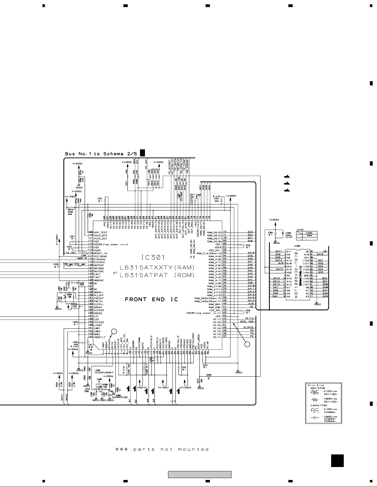
FRONT END IC
B
12
C
18
D
16
E
25
F
24
VM4-
13
VM4+
12
M56788AFP
10
VM3+
VM3-
9
Focus, Tracking,
Stepper and
Loading Drive
VM1+
VM1-35VM2-31VM2+32VM5-15VM5+
34
XCLOSE
OPEN
H1+
9
H1-H1-
10
H2+H2+
11
BA6664FM
H2-H2-
12
H3+H3+
13
• Spindle Drive
H3-H3-
14
• FG Detection
A1A1
7
A2A2
4
A3A3
2
IC301
• RF Demodulation
• Servo Control
• Servo Decode
• Error Correction
FACT
123
FDO
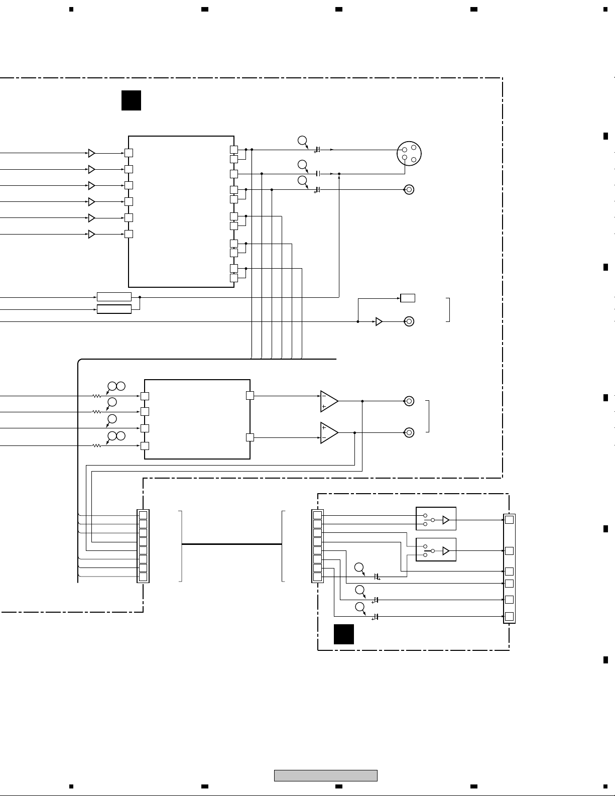
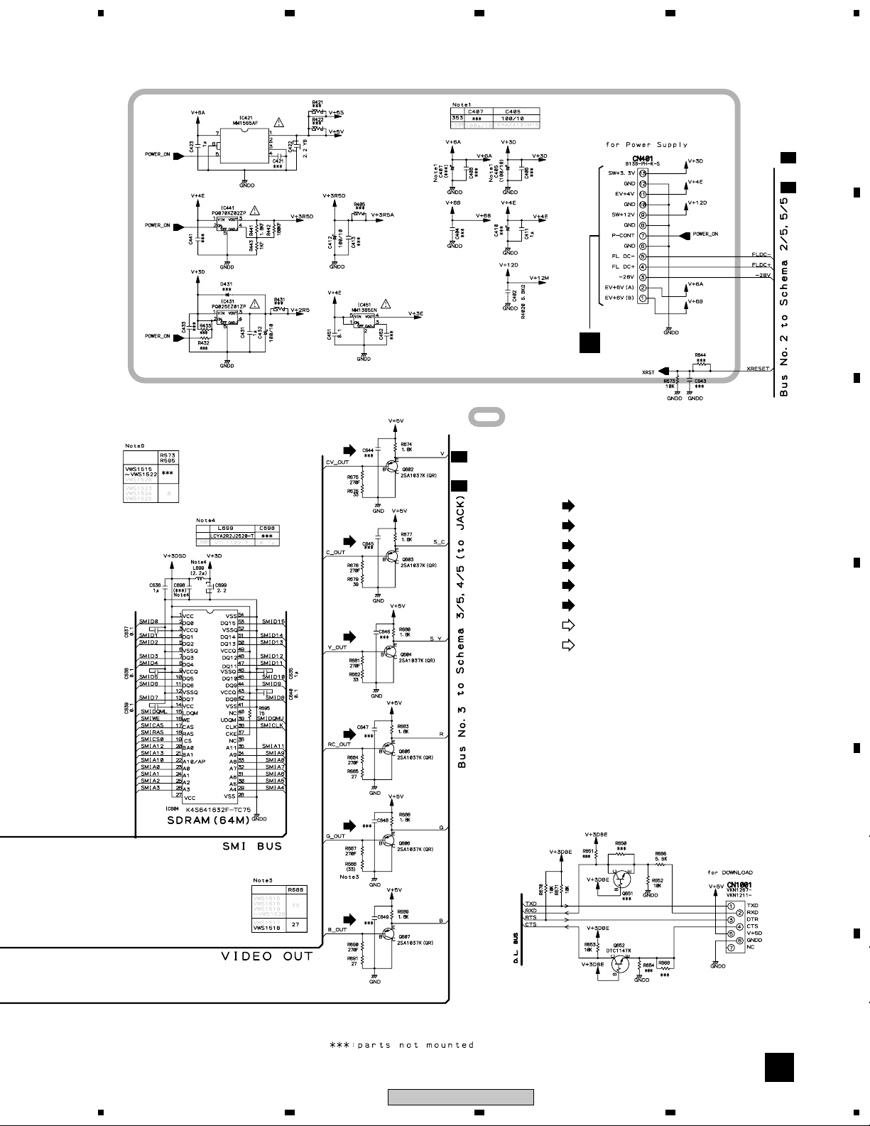
3 20
IN3-
IC351
FTS Driver
IC251
Spindle
Driver
17
CN401
(13P)
1
2
3
4
5
6
7
8
9
10
11
12
13
X301
20MHz
131
132
FREOUT FREIN
OUT_DATA(0) S_DATA
TACT
124
TDO
IN4-
IN5-
17
14
2
24
FG
EC
22
REMOTE
RECEIVER
UNIT
PC(2) PC(6)
FG
FG
SPDL PDM
X11
5MHz
C
Work RAM for MPEG Decode
K4S641632F-TC75
64M SDRAM
FE_DATA
84
4238
SPDL
PDM
LOAD_DRV
16
16
116
15
205
204
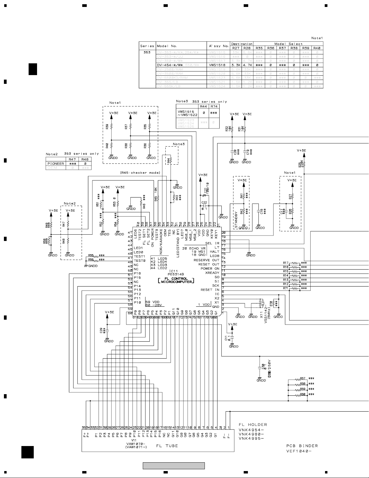
IC11 PE5314B
3
4
IC301
SPS-444L-H
FL CONTROL
X1
MICROCOMPUTER
• Main Unit Key Input
X2
• Remote Control Receive
• FL Display Control
KEY1
IR
17
21
5 2 1
IR
5 2 1
IRKY ASSY
IC604
120
PIXCLK
HSYNC
_PWM0
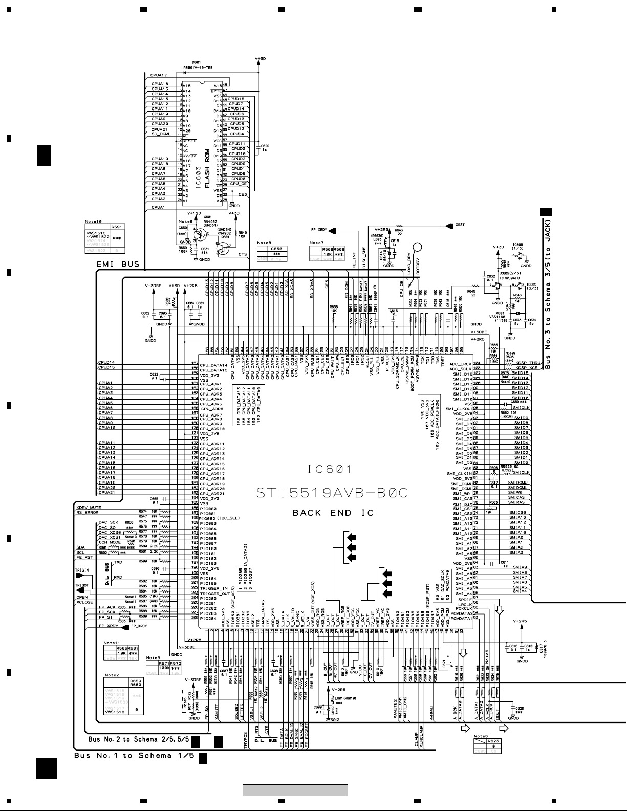
IC601
STI5519AVB-B0C
BACK END IC
• System Control
• MPEG Video Decode
• Video Encode
• Video DAC
• Audio Decode
(MP3, Dolby)
• Sub-picture Decode
XCLOSE
OPEN
8M FLASH ROM
KEY0
22
CN11
(5P)
KEY0
KEY1
CN301
(5P)
1 1
4
X601
27MHz
3562
IC605 TC7WU04FU
B_OUT
25
G_OUT
26
R_OUT
27
Y_OUT
32
C_OUT
33
CV_OUT
34
PIO381
7
PIO382
8
SPDIF
57
DAC_SCLK
PCMDATA0
IC603
VYW1978
KEY3
J301
(3P)
PCKCLK
LRCLK
V11
FL TUBE
51
52
55
56
D
PSWB ASSY
SQUEEZ
LETTER
DOUT
A_BCK
A_DATA0
A_MCLK
A_LRCK
16
1234
DV-454-K
Page 17
5
678
A
Q607
Q606
Q605
Q604
Q603
Q602
S_C
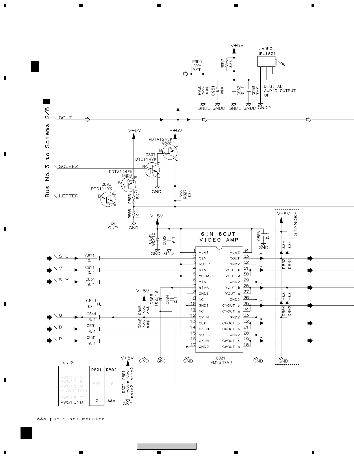
Q807,Q808
Q805,Q806
R721
R722
R723
G
R
S_Y
B
V
4 7
8
3
5 6
FJMB ASSY
B
Cb IN
14
CY IN
12
16
Cr IN
Y IN
6
C IN
2
V IN
4
MM1567AJ
6 IN • 6 OUT
VIDEO AMP
• LPF
• AMP
• Driver
BCKIN
1
DATA
2
MCLK
16
LRCKIN
3
YOUT b
IC801
Audio 2ch DAC
YOUT a
COUT
VOUT b
VOUT a
CYOUT b
CYOUT a
CrOUT b
CrOUT a
CbOUT b
CbOUT a
IC711
PCM1742KE
28
27
33
31
30
25
24
19
18
22
21
Vout L
Vout R
Y
C
V
G
R
B
Y_OUT2
C_OUT2
LOUT
7
ROUT
8
V_OUT2
G_OUT2
13
C832
14
C822
9
C812
R_OUT2
B_OUT2
AUDIO LPF
BA4560F
IC731-1/2
IC731-2/2
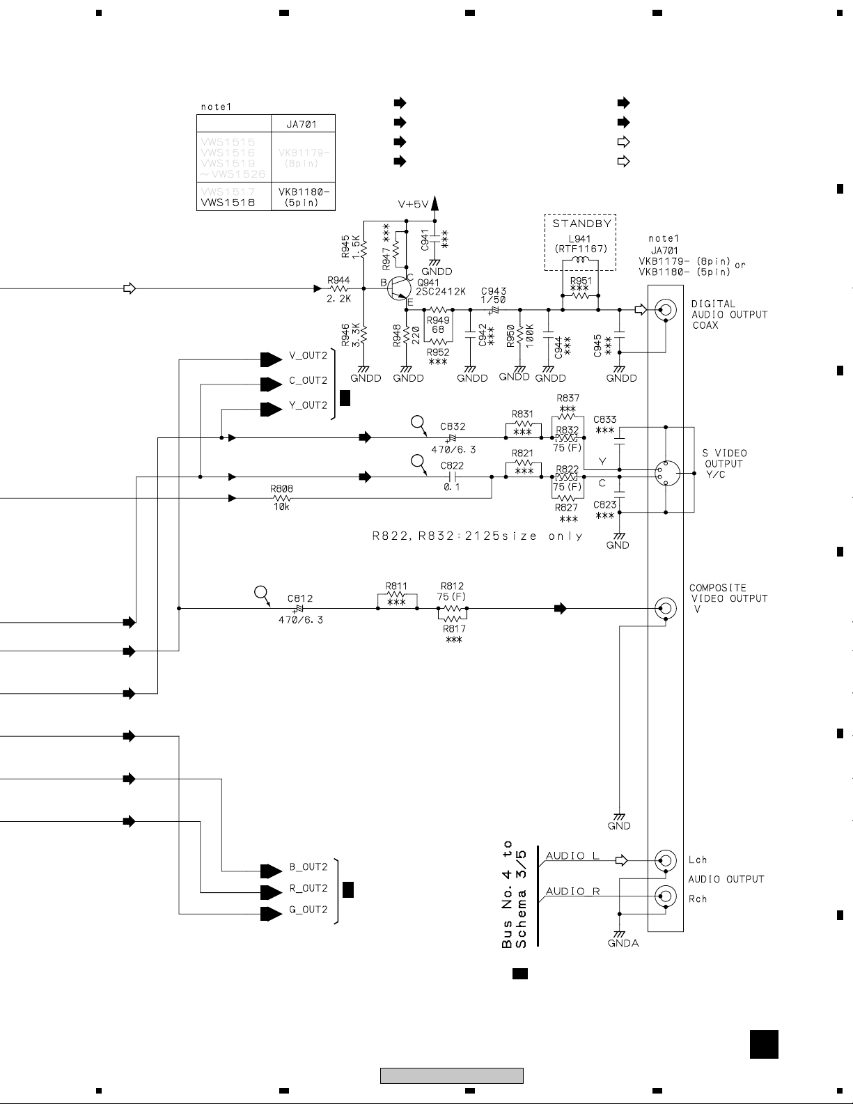
1– $: Refer to "3.1.3 WAVEFORMS".
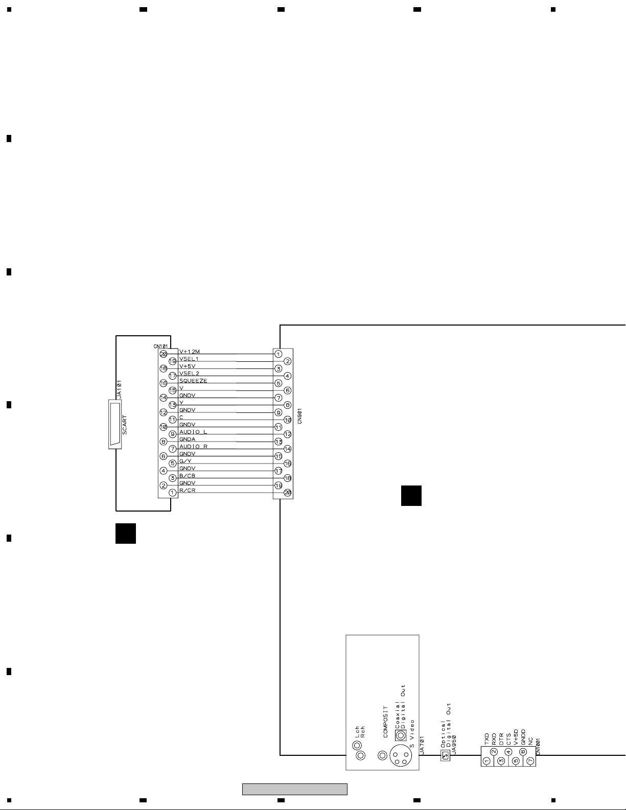
Y
C
Q941
2
1
3
5
7
6
JA950
S VIDEO
COMPOSITE
VIDEO OUT
OPTICAL
COAXIAL
L
AUDIO
OUT
R
DIGITAL
OUT
B
C
V_OUT2
Y_OUT2
C_OUT2
FRONT_L
FRONT_R
G_OUT2
B_OUT2
R_OUT2
6
8
10
12
14
16
18
20
V
Y
C
AUDIO_L
AUDIO_R
G
B
R
CN901
(20P)
AUDIO_L
AUDIO_R
D
CN101
(20P)
15
V
13
Y
11
C
9
7
G
5
B
3
R
1
10
C403
11
C501
12
C601
SCRB ASSY
G
IC301 MM1507XN
46H
IC401 MM1505XN
64L
2
L
2
H
JA101
(21P)
EURO
CONNECTOR
V/Y
19
R/C
15
AUD. LOUT
3
AUD. ROUT
1
G
11
B
7
E
F
DV-454-K
5
6
7
8
17
Page 18
1
3.1.2 POWER SUPPLY BLOCK
23
4
A
AC IN
B
POWER SUPPLY
ASSY
E
LIVE
NEUTRAL
F1
VWR1351: CN101
VWR1353: CN2
(13P)
1
2
3
4
5
6
7
8
9
10
11
12
13
EV+6V (B)
EV+6V (A)
-28V
FLDC+
FLDC-
GND
P-CONT
GND
SW+12V
GND
EV+4V
GND
SW+3.3V
CN401
1
2
3
4
5
6
7
8
9
10
11
12
13
(13P)
V+6B
V+6A
-28V
V+12M V+5AV+12D
IC421
MM1565AF
+5V Reg.
V+5S V+5V
IC901
NJM78L05A
+5V Reg.
31
2
IC431
PQ025EZ01ZP
V+3D V+2R5
+2.5V Reg.
IN OUT
FJMB ASSY
B
IC451
MM1385EN
V+4E
C
+3V Reg.
IN OUT
V+3E
IC303
BA18BC0FP
+1.8V Reg.
13
2
LOAB ASSY
A
V+3D
CN601
(5P)
4 4
CN52
(5P)
V+3R5D
IC441
PQ070XZ02ZP
+3.5V Reg.
VIN VOUT
V+3R5D V+3R5A V+1RBD V+1RBA1 V+1RBA2
D
IRKY ASSY
C
V+3E
CN301
(5P)
3 3
CN11
(5P)
V+3E
V+12M V+5V
CN901
(20P)
1 3
E
1 3
CN101
(20P)
V+12M
V+5V
SCRB ASSY
G
F
18
DV-454-K
1234
Page 19
5
678
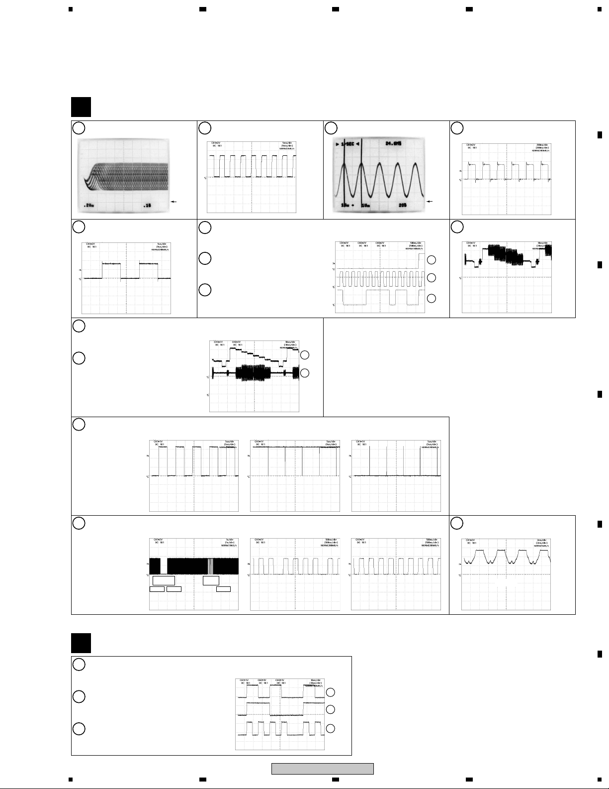
3.1.3 WAVEFORMS
Note : The encircled numbers denote measuring point in the schematic diagram.
Measurement condition
: No. 1 to 2 and 9 to 14 : reference A1 (DVD), T2-chp 19, Color-bar
No. 3 to 8 : reference A1 (DVD), T2-chp 1
FJMB ASSY
B
IC301 - pin 3 [RF]
1
V: 200mV/div. H: 0.1µsec/div.
Foot of R723 (IC711 - pin 3)
5
[AUDIO DAC -LRCK]
V: 2V/div. H: 5µsec/div.
Foot of C832 (IC801 - pin 27, 28)
13
[S Video output -Y]
V: 1V/div. H: 10µsec/div.
Foot of C822 (IC801 - pin 33)
14
[S Video output -C]
V: 1V/div. H: 10µsec/div.
GND
IC251 - pin 24 [FG]
2
V: 1V/div. H: 5msec/div.
Foot of R723 (IC711 - pin 3)
6
[AUDIO DAC -LRCK]
V: 2V/div. H: 500nsec/div.
Foot of R721 (IC711 - pin 1)
7
[AUDIO DAC -BCK]
V: 2V/div. H: 500nsec/div.
Foot of R722 (IC711 - pin 2)
8
[AUDIO DAC -DATA]
V: 2V/div. H: 500nsec/div.
(Waveform of DATA is unsettled.)
34
13
14
IC711 - pin 16 [AUDIO DAC -MCK]
V: 1V/div. H: 20nsec/div.
6
7
8
GND
Foot of R721 (IC711 - pin 1)
[AUDIO DAC -BCK]
V: 2V/div. H: 200nsec/div.
Foot of C812 (IC801 - pin 30, 31)
9
[Composite Video output]
V: 1V/div. H: 10µsec/div.
A
B
C
IC601 - pin 116 [LOAD_DRV]
15
V: 1V/div. H: 5µsec/div.
IC301 - pin 42 [SPDL_PDM]
16
Accelertar
STOP STOPPLAY
SCRB ASSY
G
Foot of C403 (FJMB: IC801 - pin 21, 22)
10
[Video output -R]
V: 2V/div. H: 10µsec/div.
Foot of C501 (FJMB: IC801 - pin 24, 25)
11
[Video output -G]
V: 1V/div. H: 10µsec/div.
Foot of C601 (FJMB: IC801 - pin 18, 19)
12
[Video output -B]
V: 2V/div. H: 10µsec/div.
5
[Tray stops] [Tray is opening] [Tray is closing]
[STOP→PLAY→STOP] [STOP]
ON
Brakes
ON
GND-R(0)→
GND-G(-)→
GND-B(=)→
[PLAY]
V: 2V/div. H: 500nsec/div. V: 2V/div. H: 500nsec/div. V: 2V/div. H: 2msec/div.V: 2V/div. H: 1sec/div.
10
11
12
DV-454-K
6
D
CN251 - pin 12, 11, 10
17
(IC251 - pin 2, 4, 7)
[Spidle driver -A3, A2, A1]
[PLAY]
E
F
19
7
8
Page 20
1
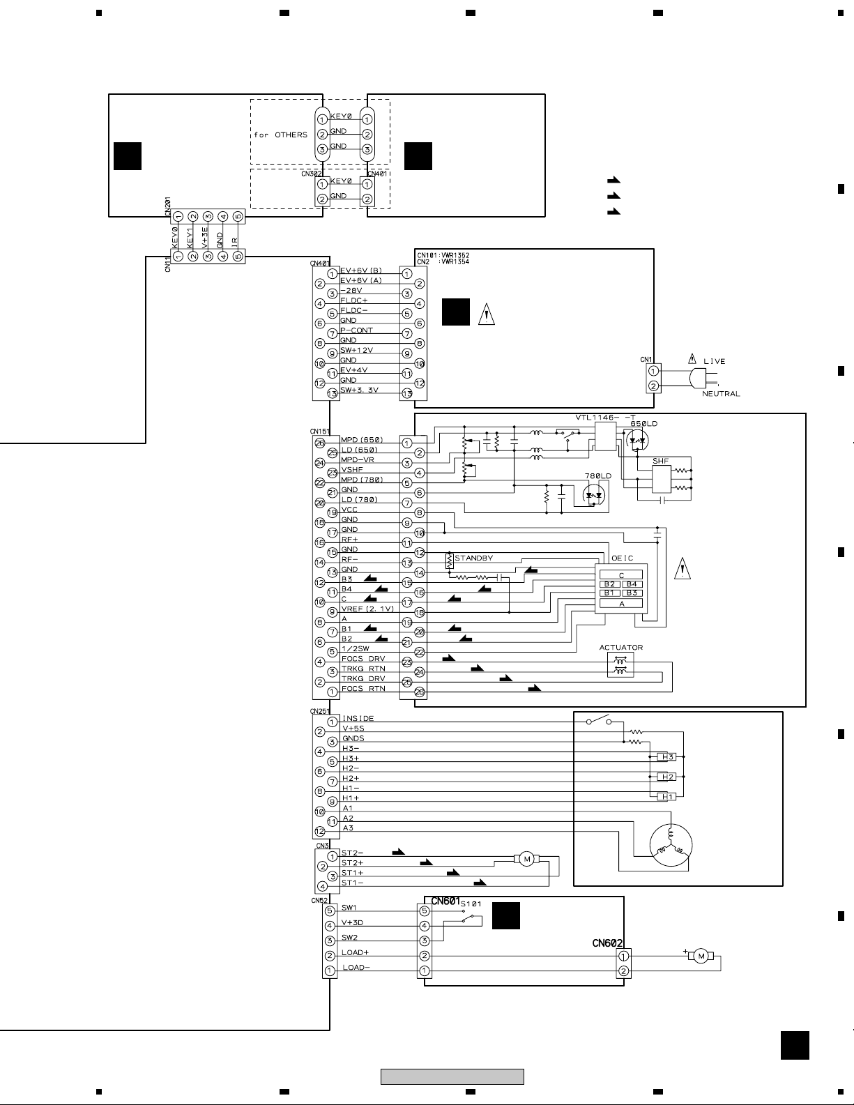
3.2 LOAB ASSY and OVERALL WIRING DIAGRAM
A
B
23
4
C
D
FJMB ASSY
B
(VWS1518)
SCRB ASSY
G
(VWV1903)
E
F
ABCDE
20
1234
DV-454-K
Page 21
5
Note : When ordering service parts, be sure to refer to "EXPLODED VIEWS and PARTS LIST" or "PCB PARTS LIST"
678
A
IRKY ASSY
C
(VWG2344)
for ##XCN type
PSWB ASSY
D
(VWG2345)
E
POWER SUPPLY UNIT
(VWR1352 or VWR1354)
(F)
: FOCUS SERVO LOOP LINE
(T)
: TRACKING SERVO LOOP LINE
(S)
: SLIDER SERVO LOOP LINE
B
C
(F)
(F)
(T)
(F)
(F)
(F)
(S)
(S)
(S)
(F)
(T)
(F)
(F)
(T)
(T)
STEPPING MOTOR
: VXM1090
(S)
(F)
(F)
LOAB ASSY
A
(VWG2279)
PICKUP ASSY-S
(OXX8003)
SPINDLE
MOTOR
: VXX1088
LOADING
MOTOR ASSY
: VXX2505
D
E
F
CDAB A
DV-454-K
5
6
7
8
21
Page 22
1
23
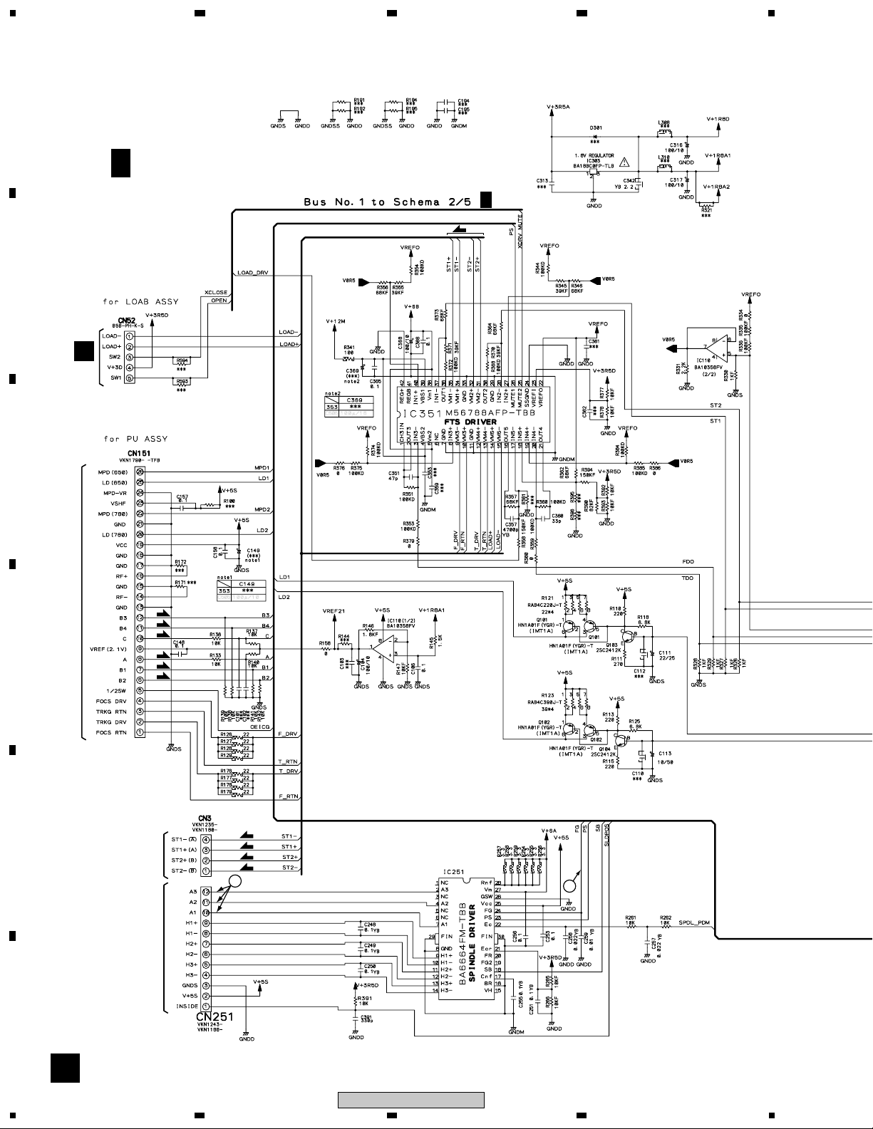
3.3 FJMB ASSY 1/5 [FRONT END BLOCK]
A
4
B 1/5
B
FJMB ASSY (VWS1518)
B
2/5
(S)
A
CN601
C
(F)
(F)
PICKUP ASSY
D
E
STEPPING
(T)
(T)
(F)
(F)
MOTOR
17
(S)
(S)
(S)
(S)
2
SPINDLE
MOTOR
F
1/5
B
22
1234
DV-454-K
Page 23
5
678
A
B
B
2/5
1, 2, #, $: Refer to "3.1.3 WAVEFORMS".
(F)
: FOCUS SERVO LOOP LINE
(T)
: TRACKING SERVO LOOP LINE
(S)
: SLIDER SERVO LOOP LINE
VCC33DAC
C
454
D
1
VCC18MN
16
E
(F)
(F)
(F)
(F)
(T)
(T)
F
1/5
B
DV-454-K
5
6
7
8
23
Page 24
1
23
3.4 FJMB ASSY 2/5 [BACK END BLOCK]
A
VYW1978
4
FJMB ASSY
(8M)
B 2/5
B
C
(VWS1518)
3/5
B
454
454
15
D
(B)
(G)
(R)
(S_Y)
(S_C)
(V)
E
454
454
F
2/5
B
24
1234
B
2/5B5/5
B
1/5
DV-454-K
(D)
(D)
454
Page 25
5
678
A
5/5
B
2/5
B
B
E
VWR1352: CN101
VWR1354: CN2
: The power supply is shown with the marked box.
(V)
454
(S_C)
(S_Y)
4/5
B
3/5
B
@: Refer to "3.1.3 WAVEFORMS".
(V)
: V SIGNAL ROUTE
(S_C)
: S-VIDEO OUT C SIGNAL ROUTE
(S_Y)
: S-VIDEO OUT Y SIGNAL ROUTE
(R)
: R SIGNAL ROUTE
(G)
: G SIGNAL ROUTE
(B)
: B SIGNAL ROUTE
: AUDIO SIGNAL ROUTE
(D)
: AUDIO(DIGITAL) SIGNAL ROUTE
C
D
(R)
(G)
E
(B)
F
2/5
B
DV-454-K
5
6
7
8
25
Page 26
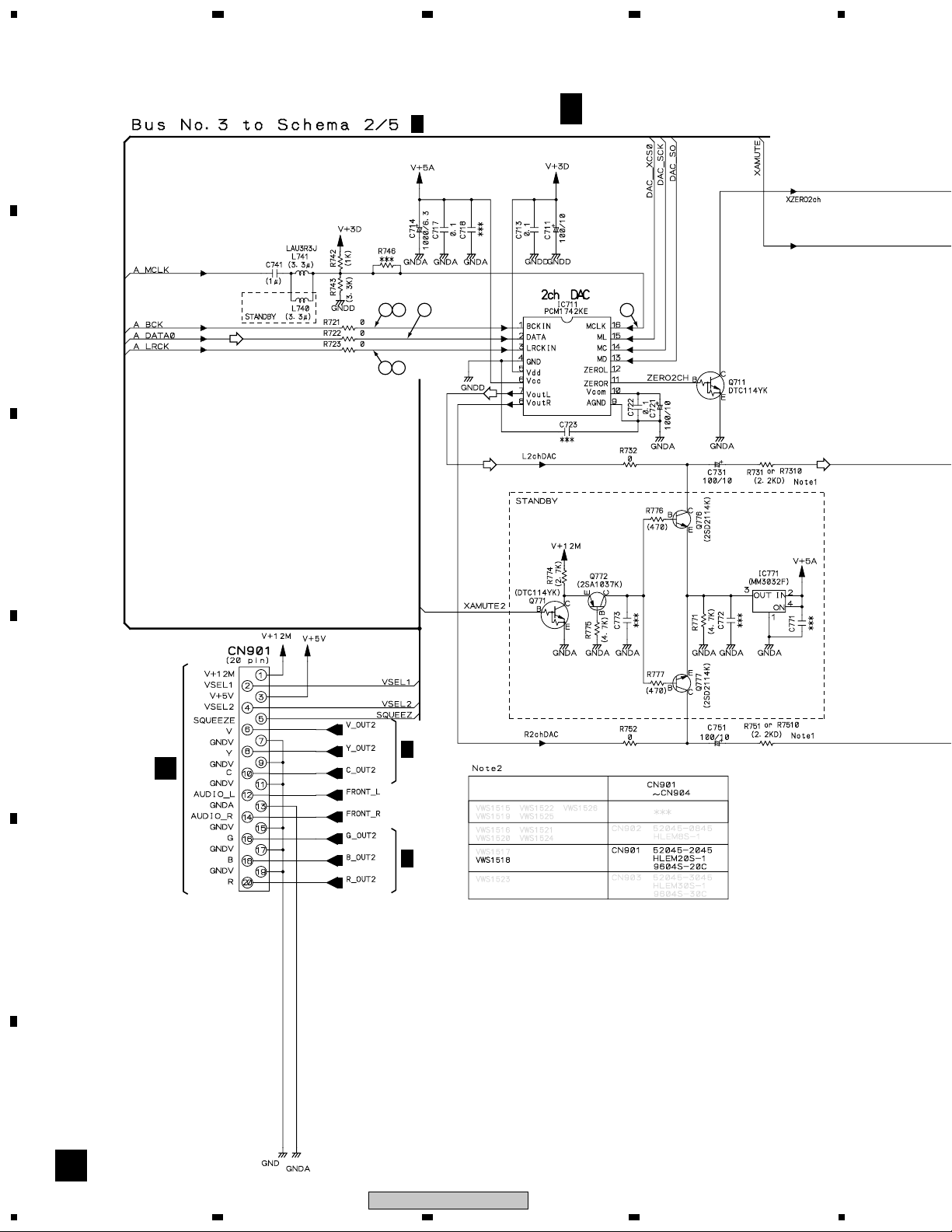
1
23
3.5 FJMB ASSY 3/5 [AUDIO BLOCK]
4
A
B
2/5
B
C
4 87
5 6
B 3/5
FJMB ASSY (VWS1518)
3
D
B
4/5
G
CN101
B
4/5
E
F
26
B
3/5
DV-454-K
1234
Page 27
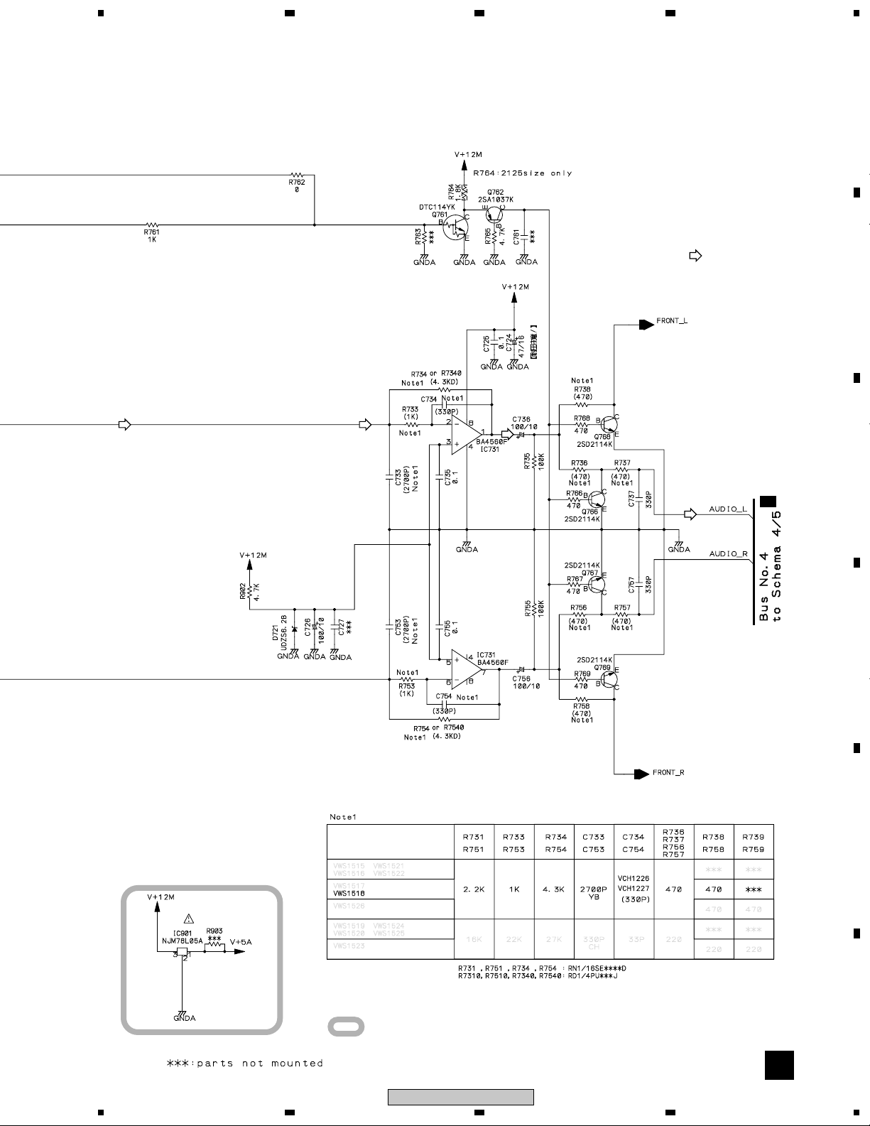
5
678
A
3– 8: Refer to "3.1.3 WAVEFORMS".
: AUDIO SIGNAL ROUTE
B
4/5
B
C
D
E
: The power supply is shown with the marked box.
3/5
B
DV-454-K
5
6
7
8
27
F
Page 28
1
23
3.6 FJMB ASSY 4/5 [VIDEO BLOCK]
A
4
B 4/5
FJMB ASSY (VWS1518)
(D)
2/5
B
B
C
(D) (D) (D)
(S_C)
D
E
F
(V)
(S_Y)
(G)
(B)
(R)
(S_C)
(V)
(S_Y)
(G)
(B)
(R)
28
B
4/5
DV-454-K
1234
Page 29
5
678
(D)
B
(S_Y)
(S_C)
3/5
(V)
: V SIGNAL ROUTE
(S_C)
: S-VIDEO OUT C SIGNAL ROUTE
(S_Y)
: S-VIDEO OUT Y SIGNAL ROUTE
(R)
: R SIGNAL ROUTE
13
14
(G)
: G SIGNAL ROUTE
(B)
: B SIGNAL ROUTE
: AUDIO SIGNAL ROUTE
(D)
: AUDIO(DIGITAL) SIGNAL ROUTE
(D)
A
B
C
(S_C)
(S_Y)
(G)
(B)
(R)
9
(V)
(V)
D
E
B
3/5
3/5
B
9, ~, !: Refer to "3.1.3 WAVEFORMS".
4/5
B
DV-454-K
5
6
7
8
29
F
Page 30
1
23
3.7 FJMB ASSY 5/5 [FL CONTROL BLOCK]
A
4
B 5/5
B
C
FJMB ASSY (VWS1518)
D
E
(XJ)
F
(XU, XQ)
(XCN)
30
B
5/5
DV-454-K
1234
Page 31

5
678
A
B
A
CN601
454 454
C
454
2/5
B
D
E
F
5/5
B
DV-454-K
5
6
7
8
31
Page 32

1
3.8 IRKY and PSWB ASSYS
A
23
4
S301 : 0 OPEN/CLOSE
S302 : 3
S303 : 8
B
S304 : 7
S305 : ¡¢
S306 : 41
B 5/5
CN11
C
IRKY ASSY
C
(VWG2344)
D
E
F
32
C
DV-454-K
1234
Page 33

5
VKP2277
678
A
B
PSWB ASSY
D
(VWG2345)
S401 : STANDBY/ON
VKP2277
for ##XCN type
C
D
E
: The power supply is shown with the marked box.
F
D
DV-454-K
5
6
7
8
33
Page 34

1
23
3.9 POWER SUPPLY UNIT (VWR1352)
A
CN101
1.6A
2.0A
B
AEK7066
AEK7067
B 2/5
1.6A
AEK7012
4
CN401
C
D
E
800mA
AEK7063
250V T2AH
REK1101
2A
POWER SUPPLY UNIT (VWR1352)
F
E
• In case of repairing, use the described parts only to prevent an accident.
• Please write the red mark on the board when the primary section of POWER SUPPLY (SYPS) Unit is repaired.
• Please take care to keep the space, not touching other parts when replacing the parts.
NOTE OF SPARE PARTS IN POWER SUPPLY (SYPS) UNIT
E
34
1234
CN1
AC IN
E
DV-454-K
Page 35

5
678
3.10 POWER SUPPLY UNIT (VWR1354)
B 2/5
800mA
AEK7063
CN401
AEK7066
2.0A
AEK7067
1.6A
1.6A
AEK7066
A
CN2
B
2.5A
REK1102
T2.5AH 250V
CN1
C
D
E
AC IN
POWER SUPPLY UNIT (VWR1354)
• In case of repairing, use the described parts only to prevent an accident.
• Please write the red mark on the board when the primary section of POWER SUPPLY (SYPS) Unit is repaired.
• Please take care to keep the space, not touching other parts when replacing the parts.
NOTE OF SPARE PARTS IN POWER SUPPLY (SYPS) UNIT
E
E
5
F
E
DV-454-K
6
7
8
35
Page 36

1
3.11 SCRB ASSY
23
4
A
B
C
SCRB ASSY(VWV1903)
G
D
B 3/5
CN901
E
F
10
36
G
DV-454-K
1234
Page 37

5
12
678
A
B
11
C
D
E
: The power supply is shown with the marked box.
0– =: Refer to "3.1.3 WAVEFORMS".
F
G
DV-454-K
5
6
7
8
37
Page 38

1
A
B
23
4
C
D
E
F
38
1234
DV-454-K
Page 39

5
678
4. PCB CONNECTION DIAGRAM
NOTE FOR PCB DIAGRAMS :
1. Part numbers in PCB diagrams match those in the schematic
diagrams.
2. A comparison between the main parts of PCB and schematic
diagrams is shown below.
Symbol In PCB
Diagrams
BCE
BCE
D
Symbol In Schematic
Diagrams
BCEBCE
BCE
BCE
DGGSS
DGS
Part Name
Transistor
Transistor
with resistor
Field effect
transistor
Resistor array
3. The parts mounted on this PCB include all necessary parts for
several destinations.
For further information for respective destinations, be sure to
check with the schematic diagram.
4. View point of PCB diagrams.
Connector
Capacitor
SIDE A
P.C.Board
Chip Part
SIDE B
A
B
4.1 LOAB ASSY
3-terminal
regulator
LOAB ASSY
A
(VNP1837-B)
C
D
E
A
M
LOADING
MOTOR
ASSY
5
CN601
CN52
B
SIDE A SIDE B
6
DV-454-K
7
F
A
39
8
Page 40

1
C606
R663
5
R
R
R
VREF
N
5
E
T
4.2 FJMB ASSY
23
4
A
B
C
D
E
SIDE A
FJMB ASSY
B
V11
Q81
IC451
R593
R84
R372
R371
Q83
C366
C365
R346
R345
R356
R355
R354
R344
1732
17
32
5
1
C452
R52
GND
41 60
41
CMKM-P3X
C29
C30
60
CN52 CN1
CN52
CN15
5
51
R594
C361
22
2242
42
R384
R385
C368
IC302
C451
R47
R48
R39
R38
R74
R51
R40
R43
R36
R45
R46
61 80
C15
C22
4021
R44
IC11
R11
C14
1
IC12
5
12
R191
R362
R394
21
1
121
R386
C329
C369
C305
16
C304
116
1
IC301
C20
R37
C19
R35
21 40
120
8061
KN901
CN601
A
R192
KN902
IC351
C359
C353
R374
R391
R375
R376
C351
C324
361
36
37
37
C323
72
72
73
73
C328
R31
R32
V+4E
R318
C21
C31
201
R17
R16
X11
R15
C11
R12
R71
R70
R673
PC
C258
C257
R262
GNDS
C331
C325
1
18
R317
L324
8
R320
R319
R27
R325
R324
5
CN11
5
10
CN12
R14
R13
R644
R73
R72
C643
R266
C251
R261
C18
R265
C17
C330
R28
1
12
C255
30
28 15
C253
C256
108
16 9
16
9
C319
R312
IC304
R314
R62
L61
13
13
SEDR+
L-POS
D-SENS
T-POS
C277
C276
1
IC271
252714
1
R297
Cross-grain
15
30
28
1
108
SEDR-
14 27
25
R305
C302
R326
144
144
C332
C322
109
109
7
8
R296
C311
C326
V+3D
GNDM
R301
R322
C340
C316
C321
R310
R349
CN16
26 13
1
direction
14
29
1
C301
C333
C327
R309
R306
14
29
1
R333
R332
R304
261
2
R298
V+5S
IC251
R154
C106
R330
C630
1
L274
L271
C274
R147
+
V
Q601
R290
C271
R289
R153
R145
E
4
X601
C278
L272
IC110
C629
R152
Q105
R149
R647
CN61
2548
C317
IC605
R640
C633
C111
4
5
C614
R641
D601
C631
R639
Q271
R271
R151
4
R567
R150
C113
815
D301
C651
R643
1
8
R564
1
4
4
C641
CN251
R111
R125
C110
1
IC603
R276
C112
R273
R146
R405
R648
Q104
8
8
5
5
Q103
C104
IC303
C313
C604
R118
171
17
X301
C632
R645
C634
R646
25
48
R272
R128
R129
1
R123
4
5
5
C108
C342
R565
C616
R642
C613
CN6011
242
C615
R638
C603
242
CN6012
241
124
R275
Q272
M
CN3CN251
R177
R178
R179
R127
R126
Q101
R121
Q102
R110
R142
1
IC111
4
C650
1
C640
R695
8
8
C635
R630
R566
105
105
123
123
156
156
242
FJMB
SPINDLE MO
M
GND
RF+
MPD78
LD65
MPD65
VCC
LD78
GND
GND
VSHF
GND
MPDVR
R176
CN3
1
1
R141
28
28
54
54
104
157
123
157
R547
4
4
R100
GND
IC604
104
IC601
CN6013
C157
R115
R662
26
26
25
25
C102
R156
R155
C636
R172
27
1
R113
27
1
C605
ST
RF-
GND
C158
R171
C103
C639
C638
C637
R574
CN1
C107
B3
C149
R588
B4
G
C
R589
CN11
CN301
C
(VNP1867-C)
Q83Q81
IC302
IC12 Q601IC271
IC301IC11IC451
IC351
IC304
IC251 Q105
IC110
IC605
Q104 IC604
IC303
IC603Q271 Q272
Q102
IC111
Q101Q103
IC601
F
B
40
1234
DV-454-K
Page 41

5
VSHF
678
NDLE MOTOR
STEPPING MOTOR
M
CN151
B4CB3
RF-
GND
GND
RF+
MPD78
VCC
LD78
GND
GND
C157
00
D
04
601
R662
26
26
R115
R156
R155
25
25
C102
R172
27
1
C636
GND
1 27
C605
R113
C158
R171
C103
C639
C638
C637
R574
CN151
C149
C107
R588
A
VREFB11/2SW
1
C148
GND
R622
R624
R619
C611
C606
R589
R663
R590
2
2
1
R133
C412
208
B
PICKUP
ASSY
T DRV
F RTN
T RTN
F DRV
B2
12
1
IC441
C407
C441
C620
R623
R625
53
53
52
52
R613
1
1
208
R552
R665
R583
R575
R602
R584
CN401
75
C423
14
1
C422
R433
D431
C433
C432
R741
C741
R621
R620
C610
R561
R558
R612
C609
R687
C608
C607
R553
R551
R543
R586
R661
R585
R587
R658
R581
R577
L740
R562
C617
C619
R580
CN401
57
IC421
4
C421
GND
C431
IC431
R746
R556
R675
R681
R688
Q606
R690
R691
R572
R591
R579
R578
R601
C410
R743
L741
R722
R554
R432
Q604
R659
R721
R676
Q602
R682
Q607
13
R557
R544
R684
DCFC
13
R678
Q605
VWR1352: CN101
E
VWR1354: CN2
44
V+5V
44
C405
1
R723
20
R576
V+12M
1
CN950
SIDE
R685
Q603
R660
R542
R901
PRINTED
R679
Q711
IC711
C723
C718
10 20
C711
V+5V
IC921
GND
WARNING
THIS PRODUCT CONTAINS LEAD IN SOLDER
AND CERTAIN ELECTRICAL PARTS
CONTAIN CHEMICALS WHICH ARE
KNOWN TO
TO CAUSE
OTHER REPRODUCTIVE HARM.
HEALTH & SAFETY CODE SECTION
25249.2
CN903
C771
IC771
C721
C772
C722
916
916
18
C717
81
C713
Q772
C714
Q771
A
+5
V
8
8
CN951
GND
C801
C644
R674
C645
R677
R680
R686
C844
C646
C647
R683
C648
THE STATE OF CALIFORNIA
CANCER,BIRTH DEFECTS OR
- PROPOSITION 65
R775
IC901
C731
1
1
R771
C773
R773
C649
C841
CN901
R734
R7310
C751
R7510
R726
C802
C851
C861
R689
CN901
CN902
R733
Q796
C755
R761
R7340
R753
R754
C794
R774
C726
C821
117
C733
C753
R7540
C811
C831
C735
C724
C795
C754
R793
C803
R944
R945
C734
R764
C805
1
8
Q794
1834
R946
IC731
R763
D803
D802
C862
IC801
Q941
R947
C725
Q795
D804
D801
CN904
Q762
R762
Q761
Q791Q792
R794
C941
R765
C761
R795
R948
R949
G
C822
R952
R738
C736
C756
C943
CN101
1
1
R758
Q766
R766
Q767
R767
C852
C842
C812
C832
6
R822
L941
R808
C951
KN903
7
R955
JA701
1012
8
R827
R821
Q768
R768
R769
JA702
3
4
Q769
JA950
CN1001
9
1
5
2
7
1
SIDE A
71
A
B
C
D
E
604
601 Q606
IC441 Q711
IC431
5
IC421
Q602
Q607
Q605
Q603
IC711 Q772
Q771Q604
IC921
6
IC771
IC901
DV-454-K
Q796
Q762 Q768
Q761
Q795 Q767
IC801
Q941
7
Q769IC731
Q766Q791Q792Q794
F
B
41
8
Page 42

1
8
Q
7
3
23
4
A
B
C
D
E
SIDE B
R865
C843
R812
R817
C757
R811
7
1
C813
R956
C758
R855
C953
R847
C823
C945
CN1001
R735
C737
R757
+12V
R739
R755
R844
R843
R837
R957
R831
C952
R756
R951
1
VSEL1
L861
+5V
VSEL2
C833
CN904
SQUEEZE
GNDV GNDV
VYC
C738
R759
R737
R736
C853
R853
R854
R857
C863
R864
R863
R867
R832
C944
R950
C942
GND
GNDA
AUDIO_L
AUDIO_R
L851
R805
G/Y
CN902
GND
B/CB
R797
R730
R806
R/CR
R796
D721
R807
ASPECT
+5V
C727
GND
CN901
R902
C804
Q806
GNDA
+12V
R802
+5V
R731
R801
Q808
GND
+3V
R732
R751
R846
Q805
CN903
GNDD
DACSO
DACSCK
Q776
Q777
R777
MCLK
1
Q807
R668
R666
R671
ALRCK
CN951
R845
ADATA1
ABCK
R776
R670
ADATA2
R752
R903
6CHMODE
DACXCS0
NC
R744
8
+12V
GNDA
Q652
XAMUTE2
XAMUTE
MIC
R921
MIC
GNDA
R653
R651
R654
MICON2
44
+3V
GNDA
20
R710
XNOR/KARA
ECHOVR
R650
C406
1
CN950
DACSO
DACSCK
GNDD
ADATA0OUT
LRCLKOUT
KDSPTHRU
KDSPXCS
XRESET
GND
R652
13
MCLK
GNDD
GNDD
LRCLKIN
ADATA0IN
BCKIN
BCKOUT
GNDA
44X48
MIC
R745
+5V
+5V
Q651
L601
C402
V
V+3D
C618
C411
+12M
R607
R560
CN401
V+12D
V+4E
V+3D
R742
V+12M
V+5V
R559
C408
R441
R422
R609
FLDC-
R443
R605
R571
R431
V+2R5
FLDC+
-28VP-CONT
R442
R545
R608
R582
12
C601
R610
R600
R421
C413
GND
C602
C621
GND
R541
C612
000
-A1
C404
ST1-
V+6B
V+12M
V+6A
V+5S
C101
R136
222
111
FJMB
ST1+
ST2-
ST2+
R138
R139
L592
R596
GND
R563
555
444
333
L603
274
6
Q273
R283
Q776
Q777
Q808 Q807
Q806
Q805
Q652 Q2
Q651
Q27
F
B
42
1234
DV-454-K
Page 43

5
678
C404
GND
D
111
000
-A1
FJMB
ST1-
ST2+
ST1+
V+6B
V+12M
V+6A
V+5S
R138
C101
R136
L592
R596
R563
444
333
222
ST2-
R139
GND
L603
555
4
CN3
V+5S
V+4E
V+3R5D
V+3DSD
777
666
Q274
R286
Q273
R283
1
GNDS
V+5S
H3-
INSIDE
V+3D
C698
R631
R632
R604
C622
R568
VWS
999
888
H3+
R546
R569
R285
R282
H2-
R140
R281
C391
117
H1-
H2+
H1+
A3
A2
A1
ST2-
R137
R157
L699
C699
R603
ST2+
R570
CN251
ST1-
ST1+
R158
ST1+
R144
CN61
EV3
GND
-28V
FLDC+
FLDCP-ON
LT1
XRESET
XREADY
S(FtoM)
S(MtoF)
SCK
GND
V+6B
V+12M
V+6A
L310
R327
R321
R573
R595
R316
R328
R299
R331
C299
C248
C249
R254
R329
C250
L308
R293
R255
C272
R291
R256
R302
C336
R339
R340
R257
R350
R294
Q275
R258
R303
113
C194
C334
R336
C195
C310
1
R259
KEY0
C335
CN11
R194
R195
KEY1
C309
EV3IR
C337
R315
GND
R22
R21
C13
R20
R19
C12
L300
IR
CN12
C259
5
R25
R300
C308
R313
R311
Q300
GND
V+3E
R307
C307
R308
R335
R26
R341
R42
R90
CN15
15
R360
R357
R351
R353
R379
R334
V+6B
R41
R18
R24
R23
CN52
C357
R392
R50
R396
R395
C360
R49
R54
R380
R53
GND
R361
FJMB ASSY
B
SW2
LOAD-
V+3D
SW1
LOAD+
R377
R378
R368
R55
R373
R81
C362
R82
R364
R56
0
1
R359
R370
R390
R393
R358
SIDE B
R83
Q82
C81
0
0
123
1
0
123456789
CBA
R57
R58
R59
R60
A
B
C
D
E
Q274
Q273
(VNP1867-C)
Q300
Q82
Q275
F
B
DV-454-K
5
6
7
8
43
Page 44

1
4.3 IRKY and PSWB ASSYS
A
PSWB ASSY
D
23
4
VWG2345-
PSWB
VWG
POWER ON
S401
CMKS-P3X
B
31
1
1
for ##XCN type
1
CN302
REV
S306
S305
1
1
CN401
1
for OTHERS
PC
31
CMKS-P3X
IRKY
VWG2344-
VWG
IRKY ASSY
C
S304
S303
L321
OPEN/
CLOSE
PLAYPAUSESTOPFWD
S302
S301
5
5
CN301
1
C302
54
31
IC301
21
CN301
CN11
B
C
SIDE A
(VNP1868-B)
SIDE B
D
1
2.3.GND
31
E
D
(VNP1868-B)
CN302
1
1.KEY0
1
CMKS-P3X
REV
POWER ON
PSWB ASSY
FWD
R313R314
VWG
VWG2345-
PSWB
GND
1
IRKY
VWG
VWG2344-
1
1
KEY0
CN401
KEY0
GND
GND
3
31
STOP
CMKS-P3X
R312
IRKY ASSY
C
PAUSE
R321
R311
R303
R301
R302
PLAY
CN301
CLOSE
OPEN/
KEY0
KEY1
V+3E
GND
IR
51
R322
R323
C301
D301
F
C D
44
DV-454-K
C D
1234
Page 45

5
678
4.4 POWER SUPPLY UNIT (VWR1352)
SIDE A SIDE A
AC IN
POWER SUPPLY UNIT
E
Q2
A
B
C
Q1
Q20
Q320
IC103
IC201
Q412
VR201
CN401
B
CN101
D
E
E
Q411
Q410
F
E
DV-454-K
5
6
7
8
45
Page 46

1
23
4.5 POWER SUPPLY UNIT (VWR1354)
4
A
B
C
SIDE A SIDE A
AC IN
POWER SUPPLY UNIT
E
IC3
IC2
D
IC1
IC4
CN401
B
CN2
E
F
E
46
Q6
E
DV-454-K
1234
Page 47

5
4.6 SCRB ASSY
Production
Code
678
A
SCRB ASSY
G
PYKC F6
SIDE A
SIDE B
W121
W120
W119
GNDV
W118
+5V
(VNP1868-B)
(VNP1868-B)
JA101
SCRB
VWV1902VWV1903-
VWV
GNDV
GNDV
W116
W117
GNDV
+12V
AUDIO_L
NC
AUDIO_R
GNDV
GNDV
CN101(20P)
20.+12V
18.+5V
W115
W114
16.SQUEEZE
14.GNDV
12.GNDV 11.C
10.GNDV 9.AUDIO_L
8.GNDA 7.AUDIO_R
6.GNDV 5.G/Y
4.GNDV 3.B/CB
2.GNDV 1.R/CR
GNDA
C601
W113
+5V
SQUEEZE
BNCGNDV
19.VSEL1
17.VSEL2
15.V
13.Y
GNDV
C501
W112
NC
+5V
NC
GNDV
GNDV
G
C404
W111
W110
GNDV
R/C
BLANK
GNDV
V/Y
NC
GNDV
CN102(14P)
11.VSEL2
9.V
7.Y
5.C
3.AUDIO_L
1.AUDIO_R
W103
C403
C304
W109
W108
14.+12V 13.VSEL1
12.+5V
10.SQUEEZE
8.GNDV
6.GNDV
4.GNDV
2.GNDA
+5V
W102
GNDV
W107
R
W101
VSEL2
AUDIO_L
GNDA
W106
14
AUDIO_R
W105
W104
SIDE
C111
20
2010
CONTACT
CN102
1
1
CN101
1
B
CN901
B
CN101
C
Q201
Q202
R203
+5V
C102
R104
R108
R107
R106
R201
C201
C202
R202
R204
R206
R205
C203
+12V
GNDV
R101
D101
R109
C103
GNDV
GNDV
C101
Q101
R103
R102
Q102
C902
1
R902
R901
C901
2
R105
R801
C801
R701
2.GNDV
4.GNDV
6.GNDV
8.GNDA
10.GNDV
12GNDV
14.GNDV
16.SQUEEZE
18.+5V
20.+12V
+5V
D601
D602
R601
R603
C701
C602
R602
R501
R503
1.R/CR
3.B/CB
5.G/Y
7.AUDIO_R
9.AUDIO_L
11.C
13.Y
15.V
17.VSEL2
19.VSEL1
+5V
D501
D502
R502
D401
+5V
D402
R401
C502
R403
CN101(20P)
2.GNDA
4.GNDV
6.GNDV
8.GNDV
10.SQUEEZE
12.+5V
14.+12V
1
3
R402
R303
C405
R301
6
4
C401
R302
IC401
D302
C305
CN102(14P)
1.AUDIO_R
3.AUDIO_L
5.C
7.Y
9.V
11.VSEL2
13.VSEL1
1
3
D301
+5V
21
20
AUDIO_R
GNDA
C402
C302
C303
14
SCRB ASSY
R
IC301
GNDV
G
AUDIO_L
6
4
VSEL2
C301
VWV
1
CN101
1
CN102
20
D
E
VWV1903VWV1902-
SCRB
F
G
G
DV-454-K
5
6
7
8
47
Page 48

1
23
5. PCB PARTS LIST
NOTES:•Parts marked by "NSP" are generally unavailable because they are not in our Master Spare Parts List.
Mark No. Description Part No.
A
The mark found on some component parts indicates the importance of the safety factor of the part.
•
Therefore, when replacing, be sure to use parts of identical designation.
When ordering resistors, first convert resistance values into code form as shown in the following examples.
•
Ex.1 When there are 2 effective digits (any digit apart from 0), such as 560 ohm and 47k ohm (tolerance is shown by J=5%,
and K=10%).
560 Ω→56 × 10
47k Ω→47 × 10
0.5 Ω→R50 ..................................................................................... RN2H
1 Ω→1R0 ..................................................................................... RS1P 1 R 0 K
Ex.2 When there are 3 effective digits (such as in high precision metal film resistors).
5.62k Ω→ 562 × 10
1
→ 561 ........................................................ RD1/4PU 5 6 1 J
3
→ 473 ........................................................ RD1/4PU 4 7 3 J
1
→ 5621 ...................................................... RN1/4PC 5 6 2 1 F
Mark No. Description Part No.
R 5 0
4
K
Mark No. Description Part No.
B
7 LIST OF ASSEMBLIES
NSP 1..LOADING MECHANISM ASSY VWT1197
NSP 2..LOAB ASSY VWG2279
1..FJMB ASSY VWS1518
NSP 1..KEYB ASSY VWM2122
NSP 2..IRKY ASSY VWG2344
NSP 2..PSWB ASSY VWG2345
> 1..POWER SUPPLY UNIT VWR1354
C
D
1..SCRB ASSY VWV1903
(or VWR1352)
Mark No. Description Part No.
7 PCB PARTS LIST
LOAB ASSY
SWITCHES AND RELAYS
S101 REAF SWITCH VSK1011
OTHERS
CN602 CONNCTOR S2B–PH–K
CN601 CONNCTOR S5B–PH–K
PRINTED CIRCUIT BOARD VNP1837
FJMB ASSY
SEMICONDUCTORS
IC110 BA10358FV
> IC303 BA18BC0FP
IC731 BA4560F
IC251 BA6664FM
IC604 K4S641632F–TC75
IC302 K6T1008V2E–TB70
IC301 L6315ATXXTY
IC351 M56788AFP
> IC451 MM1385EN
> IC421 MM1565AF
> IC901 NJM78L05A
> IC431 PQ025EZ01ZP
> IC441 PQ070XZ02ZP
E
F
48
1234
DV-454-K
IC801 MM1567AJ
IC711 PCM1742KE
IC11 PE5314B
IC12 PST3228
IC601 STI5519AVB–B0C
IC605 TC7WU04FU
IC603 VYW1978
Q300, Q602–Q607, Q762 2SA1037K
Q81, Q83 2SA1602A
Q103, Q104, Q82, Q941 2SC2412K
Q766–Q769 2SD2114K
Q652 DTC114TK
Q711, Q761, Q805, Q807 DTC114YK
Q101, Q102 HN1A01F
Q806, Q808 PDTA124EK
Q601 RN4982
D601 RB501V–40
D721 UDZS6.2B
Page 49

5
678
Mark No. Description Part No.
COILS AND FILTERS
L741 LAU3R3J
L699 LCYA2R2J2520
L300 LCYA2R7J2520
L324 CHIP BEADS VTL1083
CAPACITORS
C301, C302 CCSRCH100D50
C310 CCSRCH151J50
C307 CCSRCH180J50
C360 CCSRCH330J50
C391, C737, C757 CCSRCH331J50
C351 CCSRCH470J50
C309 CCSRCH560J50
C308 CCSRCH7R0D50
C633, C634 CCSRCH8R0D50
C113 CEAT100M50
C104, C21, C316, C317, C368 CEAT101M10
C405, C412, C432, C614, C711 CEAT101M10
C721, C726, C731, C736, C751 CEAT101M10
C756, C801, C803 CEAT101M10
C617, C714 CEAT102M6R3
C943 CEAT1R0M50
C111 CEAT220M25
C724 CEAT470M16
C812, C832 CEAT471M6R3
C342, C422 CKSQYB225K10
C699 CKSQYF225Z16
C14, C340, C641 CKSRYB102K50
C259, C311 CKSRYB103K50
C248–C251, C255 CKSRYB104K16
C257, C258 CKSRYB223K50
C733, C753 CKSRYB272K50
C357 CKSRYB472K50
C106, C11, C148, C157, C158 CKSRYF104Z25
C22, C253, C256, C304 CKSRYF104Z25
C321–C333, C365, C366, C451 CKSRYF104Z25
C602–C609, C612, C618 CKSRYF104Z25
C621, C622, C632, C637–C640 CKSRYF104Z25
C713, C717, C722, C725, C735 CKSRYF104Z25
C755, C802, C804, C805, C811 CKSRYF104Z25
C821, C822, C831, C844, C851 CKSRYF104Z25
C861, C952 CKSRYF104Z25
C30 CKSRYF104Z50
C411, C423, C431, C601 CKSRYF105Z10
C610, C611, C613, C615, C629 CKSRYF105Z10
C635, C636, C741 CKSRYF105Z10
C734, C754 (330P/50V) VCH1226
RESISTORS
R121 RAB4C220J
R123 RAB4C390J
R731, R751 RN1/16SE2201D
R734, R754 RN1/16SE4301D
R341 RS1/10S101J
R764 RS1/10S182J
R126–R129, R176–R179 RS1/10S220J
R254–R259 RS1/10S3R3J
R822, R832 RS1/10S75R0F
R326–R330, R443 RS1/16S1001F
Mark No. Description Part No.
R147, R265, R266, R304, R322 RS1/16S1002F
R377, R378, R392, R393 RS1/16S1002F
R344, R351, R353, R354 RS1/16S1003D
R359, R360, R368, R372 RS1/16S1003D
R374, R375, R384, R385 RS1/16S1003D
R335, R336 RS1/16S1003F
R302 RS1/16S1202F
R358, R394 RS1/16S1503F
R146, R441 RS1/16S1801F
R612, R613 RS1/16S1802F
R442 RS1/16S1803F
R675, R678, R681, R684, R687 RS1/16S2700F
R690 RS1/16S2700F
R345, R355, R370, R371 RS1/16S3902F
R346, R356, R357, R362, R364 RS1/16S6802F
R373 RS1/16S6802F
R812 RS1/16S75R0F
R390 RS1/16S8202F
OtherResistors RS1/16S###J
OTHERS
CN901 20P CONNECTOR 52045–2045
CN401 CONNECTOR B13B–PH–K
CN11, CN52 CONNECTOR POST B5B–PH–K
JA950 JFJ1001
OPT. LINK OUT 8MB/S
V11 FL TUBE VAW1070
FLEXIBLE CABLE VDA1681
PCB BINDER VEF1040
JA701 JACK VKB1180
CN3 4P CONNECTOR VKN1180
CN251 12P CONNECTOR VKN1188
CN1001 7P CONNECTOR VKN1211
CN151 26P CONNECTOR VKN1790
FL HOLDER VNK4980
X11 (5MHz) VSS1142
X301 (20MHz) VSS1167
X601 (27MHz) VSS1168
IRKY ASSY
SEMICONDUCTORS
IC301 SPS–444L–H
COILS AND FILTERS
L301, L311 VTL1084
SWITCHES AND RELAYS
S301–S306 ASG7013
CAPACITORS
C301 CKSRYF104Z25
RESISTORS
All Resistors RS1/16S###J
OTHERS
3P CABLE HOLDER 51048–0300
J301 3P JUMPER WIRE D20PDD0315E
CN301 CONNECTOR S5B–PH–K
A
B
C
D
E
F
DV-454-K
5
6
7
8
49
Page 50

1
23
4
Mark No. Description Part No.
A
PSWB ASSY
SWITCHES AND RELAYS
S401 ASG7013
OTHERS
3P CABLE HOLDER 51048–0300
B
POWER SUPPLY UNIT (VWR1352)
OTHERS
> P103 PROTECTOR (1.6A) AEK7012
> P101 PROTECTOR (800mA) AEK7063
> P102 PROTECTOR (1.6A) AEK7066
> P104 PROTECTOR (2A) AEK7067
> F1 FUSE (2A) REK1101
POWER SUPPLY UNIT (VWR1354)
OTHERS
C
> CP5 PROTECTOR (800mA) AEK7063
> CP2, CP3 PROTECTOR (1.6A) AEK7066
> CP1 PROTECTOR (2A) AEK7067
> F1 FUSE (2.5A) REK1102
Mark No. Description Part No.
SCRB ASSY
SEMICONDUCTORS
IC401 MM1505XN
IC301 MM1507XN
D
CAPACITORS
RESISTORS
E
OTHERS
Q102, Q202 2SA1037K
Q101, Q201 2SC2412K
D101, D301, D302, D401, D402 1SS355
C701, C801 CCSRCH331J50
C403 CEAT100M50
C404, C501, C601 CEAT101M10
C304 CEAT471M6R3
C102, C103, C202, C301–C303 CKSRYF104Z25
C401, C402 CKSRYF104Z25
R301, R401, R501, R601 RS1/10S0R0J
R205 RS1/10S68R0F
R302, R402, R502, R602 RS1/10S75R0F
OtherResistors RS1/16S###J
CN101 20P CONNECTOR 52045–2045
JA101 CONNECTOR VKB1157
F
50
1234
DV-454-K
Page 51

5
1
1 2
2
3
Tangential
adjustment
screw
1 2
Radial
adjustment
screw
Adjustment Items
[Mechanism Part]
[Electrical Part]
Tangential and Radial Height Coarse Adjustment
DVD Jitter Adjustment
Initialize the Focus Sweep Setting
Electrical adjustments are not required.
Adjustment Points (Mechanism Part)
Cautions: After adjustment, adjustment screw locks with the
Screw tight.
Screwdriver (large)
TV monitor
Precise screwdriver
DVD test disc
(GGV1025)
Test mode remote control
unit (GGF1067)
Screw tight
(GYL1001)
Screwdriver (medium)
6. ADJUSTMENT
678
6.1 ADJUSTMENT ITEMS AND LOCATION
A
B
C
6.2 JIGS AND MEASURING INSTRUMENTS
D
E
5
6
DV-454-K
F
51
7
8
Page 52

1
23
6.3 NECESSARY ADJUSTMENT POINTS
A
When Adjustment Points
Exchange Parts of Mechanism Assy
4
Exchange the Pickup
Mechanical
point
~, Ÿ, !
∗ After adjustment, screw locks
with the Screw tight.
Electric
point
B
Exchange the Traverse Mechanism
Mechanical
point
!
Electric
point
Exchange the Spindle Motor
C
Mechanical
point
Electric
point
Ÿ, !
∗ After adjustment, screw locks
with the Screw tight.
Exchange PCB Assy
Exchange PC Board
Mechanical
point
LOAB, FJMB ASSY
Electric
D
point
∗
Purpose: To set the sweep which was correct with the
Be sure to perform the following step finally when replaced
Pickup, Traverse Mechanism and Spindle Motor.
E
(It is necessary when performed adjustment procedure Ÿ.)
F
individual Traverse mechanism.
ESC CLEAR
GGF1067
Test mode
remote control
unit
52
1234
DV-454-K
Page 53

5
TEST MODE: ON
TEST MODE: DISC SET
DSC -
&&&
GGF1067
Test mode
remote control
unit
GGF1067
Test mode
remote control
unit
POWER
ON
<TRAY OPEN>
OPEN/CLOSE
(Player or Remote
Control Unit)
OPEN/CLOSE
(Player or Remote
Control Unit)
DVD disc
TEST MODE: PLAY
TEST MODE: OFF
An address is displayed
For example, when playback with # 30000
During PLAY
Press keys in order
OR
ESC
OFF
POWER
030000
<PLAY>
< When playback with the target address of disc (DVD)>
TV/LDP
+10 3 0 0 0 0 CHP/TIM
ESC TEST
CHECK
DVD, CD
CAUTION:
Perform only trace, video and audio output are
nothing.
678
6.4 TEST MODE
A
B
C
D
E
DV-454-K
5
6
7
8
53
F
Page 54

1
6.5 MECHANISM ADJUSTMENT
A
Tangential and Radial Height Coarse Adjustment
1
23
4
START
• Remove the servo mechanism.
• Remove a Spacer for height adjustment
attached to the back side (shaded area)
of the Servo Mechanism (Float Base) with
nippers.
B
Servo Mechanism
Float Base
Spacer for Height adjustment
Note:
C
Turn the Short switch to Short side when
removing the Pickup Flexible Cable.
(Refer to "7.1.6 DISASSEBLY".)
Cautions:
Because there is not a Spacer for height adjustment in
adjustment after the second time, will keep it at need.
(This parts is Traverse mechanism exclusive use of a model
for 2001 years)
7.3mm
Put a spacer between a Tangential (or Radial) adjustment
screw and Mechanism Base and turn each screw to adjust
the height. (Refer to "6.1 ADJUSTMENT ITEMS AND
LOCATION".)
Turn a flat side
into bottom
D
E
F
54
1234
DV-454-K
Page 55

5
Player
Monitor
• Test mode
• Play the DVD test disc
at outer track
(around #200000)
• Play the DVD test disc
at inner track
(around #30000)
• Play the DVD test disc
at outer track
(around #200000)
Mechanism Assy
Adjust the Tangential
Adjustment Screw so that
jitter becomes minimum.
Mechanism Assy
Readjust the Tangential
Adjustment Screw so that
jitter becomes minimum.
Mechanism Assy
Adjust the Radial
Adjustment Screw so that
jitter becomes minimum.
Use disc: GGV1025
START
DVD Jitter Adjustment
2
J : - - - -
J : Min
J : Min
Test mode end
J : Min
ESC
Disc playback normally.
• The measurement of block error rate
If error rate is OK,
locks a root of
tangential and radial
adjustment screws with
the Screw tight, and
go to step
!
.
Screw tight: GYL1001
Turn the POWER OFF in
case of NG once, and
perform the adjustment
once again.
Confirm the error rate that is
displayed "OK"
(Example ERROR RATE: 6.6oe - 6 OK )
5ESC
CHECK
NG
OK
• Playback method of inner and outer address for the purpose is refererd to "6.4 TEST MODE".
• Jitter indication of the monitor is refererd to "7.1.1 TEST MODE (Display Specification of the Test Mode)".
678
A
B
C
D
E
5
F
DV-454-K
6
7
8
55
Page 56

1
A
Initialize the Focus Sweep Setting
3
23
4
Purpose: To set the sweep which was correct with the individual Traverse mechanism.
Turn on the Player
ESC CLEARPOWER
B
Note: Be sure to perform this step when replaced the Pickup or Traverse mechanism.
C
D
E
F
56
1234
DV-454-K
Page 57

5
678
7. GENERAL INFOMATION
7.1 DIAGNOSIS
7.1.1 TEST MODE
Test Mode Functional Specification
1 Test mode entry
In the power ON state, press the [ESC] (A8-5F) key and [TEST / RANDOM] (A8-5E) key in order of the LD remote control unit.
• Light the all FL and LEDs, and goes out the FL and LEDs when pressing the keys of something.
• OSD displays test mode. Refer to the "Display Specification of the Test Mode".
2 Release the Test mode
• Turn off the power.
• Press the [ESC] (A8-5F) key of the remote control unit and reset it.
3 Tray open / close
• Press the [REPEAT A-B] (A8 - 48) key of the remote control unit.
• Press the [OPEN / CLOSE] key of the main unit from the stop state.
4 Playback stop
• Press the [REPEAT] (A8 - 44) key of the remote control unit from the playback state.
5 LD ON
DVD : Press the [TEST] (A8-5E) and [1] (A8-01) keys in order, and turn on the laser diode (650n).
CD : Press the [TEST] (A8-5E) and [4] (A8-04) keys in order, and turn on the laser diode (780n).
6 Focus on / sweep
1. Lock the focus by pressing the [TEST] (A8-5E) and [2] (A8-02) keys in order.
2. Repeat focus sweep by pressing the [TEST] (A8-5E) and [3] (A8-03) keys in order.
A
B
C
7 Spindle FG servo
CAV : Press the [TEST] (A8-5E) and [5] (A8-05) keys in order,then rise up the spindle and it becomes FG servo on.
CLV : Press the [TEST] (A8-5E) and [9] (A8-09) keys in order,then rise up the spindle and it becomes FG servo on.
8 Tracking open / close
1. Open tracking by pressing the [STEP FWD] (A8-54) key of the remote control unit in the play state.
2. Close tracking by pressing the [STEP REV] (A8-50) key of the remote control unit in the play state.
9 Slider servo on/off
1. Turn on the slider servo by pressing the [TEST] (A8-5E) and [CX] (A8-0E) keys in order.
2. Turn off the slider servo by pressing the [TEST] (A8-5E) and [TV/LDP] (A8-0F) keys in order.
0 Slider in / out
Slider in : In the tracking off state, press the [SCAN REV] (A8-11) key of the remote control unit.
Slider out : In the tracking off state, press the [SCAN FWD] (A8-10) key of the remote control unit.
- Play (perform only the ID search and trace to the specified location)
Press the [TV/LDP] (A8-0F) key of the remote control unit from the stop state.
Perform only trace, video and audio output are nothing.
= Screen display ON/OFF
1. Turn off the display by pressing the [AUDIO] (A8-1E) key of the remote control unit.
2. Turn on the display by pressing the [DISPLAY] (A8-43) key of the remote control unit.
D
E
F
DV-454-K
5
6
7
8
57
Page 58

A
B
1
23
4
~ Search
1. Search address input entry
• It becomes the address input mode when pressing the [+10] (A8-1F) key. (Most significant digit of an address displays ">".)
• In this time, display the last address as the initial state.
2. Search address input
• Press the [0] to [9] (A8-00 to 09) keys of the remote control unit. In the DVD, set an address with hexadecimal.
• In the address input mode, turn to the hexadecimal input by pressing the [PROGRAM] (A8-4C) key (display a "∗" mark), and [1] to [6]
keys are each input as A to F.
• In this time, do not accept the [7],[8],[9] and [0] keys. Hexadecimal input and decimal input can switch with toggle.
• In case of CD, perform only the absolute time search.
3. Search execution
• Press the [CHP/TM] (A8-13) key of the remote control unit.
• After the search, perform only trace and video and audio outputs are nothing.
4. Release the Search address input
• Clear the address by pressing the [CLEAR] (A8-45) key. Release the address input mode when pressing the [CLEAR] key once again.
C
D
E
F
58
1234
DV-454-K
Page 59

5
678
Display Specification of the Test Mode
Character in bold : Item name
: Information display
1
5
6
13
10
11
1 Address indication
The address being traced is displayed in number.
(as for the DVD, indication of decimal number is possible.)
DVD : ID indication (hexadecimal number, 8 digits)
[∗ ∗ ∗ ∗ ∗ ∗ ∗ ∗]
CD : A-TIME (min. sec.) [0 0 0 0 ∗ ∗ ∗ ∗]
0 Disc sensing [DSC – ∗ ∗ ∗]
The type of discs loaded is displayed.
[DVD], [CD ], [VCD], [ ]
- Jitter value [J – ∗ ∗ ∗ ∗]
12
14
15
16
17
18
19
A
2
3
7
8
9
B
C
2 Code indication of remote control unit [R – ∗ ∗ ∗ ∗]
In case of double code, display a 2nd code.
3 Main unit keycode indication [K – ∗ ∗]
5 Tracking status [TRKG – ∗ ∗ ∗]
Tracking on : [ON]
Tracking off : [OFF]
6 Spindle status [SPDL – ∗ ∗ ∗]
[OFF], [A/B] (ACC/BRK), [CAV], [CLV]
7 Mechanism (loading) position value [M – ∗ ∗]
Unknown : [01] or [41]
Open state : [04]
Close state : [08]
During opening : [12]
During closing : [22]
8 Slider position [S – ∗ ∗ ∗ ∗]
CD TOC area : [IN ]
CD active area : [CD]
9 Output video system [V – ∗ ∗ ∗ ∗]
NTSC system : [NTSC]
PAL system : [PAL]
Automatic setting : [AUTO]
Scart terminal output [SK – ∗ ∗]
(Display only the WY model which can do the output setting
of scart terminal.)
VIDEO : [00]
S-VIDEO : [01]
RGB : [02]
= Version of the AV-1 chip / version of firmware
[AV: ∗ ∗ / ∗ ∗ ∗ ∗ ∗ ∗ ∗ ∗]
~ Version of the FL controller [FL: ∗ ∗ ∗ ∗]
! Region setting of the player [REG: ∗]
Setting value : [1] to [6]
@ Destination setting of the FL controller
[MDL: ∗ ∗ ∗ ∗ / ∗ ∗ ∗]
Four characters in the front represent the type of model.
Three characters in the back represent the destination code.
J: /J, K: /KU, /KC, /KU/KC, R: /RAM/RL/RD, LB: /LB,
WY: /WY
# Part number of the flash ROM
[∗ ∗ ∗ ∗ ∗ ∗]
$ Version of the flash ROM [V: ∗. ∗ ∗ ∗]
Flash ROM size [FLSH = ∗]
% Revision of the system controller [S: ∗ . ∗ / ∗ ∗ ∗ ]
^ Revision of the DVD mechanism controller
[M: ∗ / ∗ ∗]
D
E
F
DV-454-K
5
6
7
8
59
Page 60

1
23
4
A
Shortcut key Functional Specification
Only in the normal playback, the following setting can by pressing the required key after having pressed the "ESC" key of
the remote control unit. How to release: Press the "ESC" key. (function with indication)
Command Contents Conditions
Memory clear & region / revision indication CLEAR
Average value measurement of DVD error rate
CD error rate measurement
Aspect: Pan scan
Aspect: Letter box
B
C
D
Aspect: Wide
Digital: PCM
Digital: AC-3/PCM
Virtual Dolby: VDD=OFF Only correspondence model
Virtual Dolby: VDD=ON Only correspondence model
Digital output ON
Digital output OFF
DTS Digital Out ON STEP FWD AF-B7
DTS Digital Out OFF STEP REV AF-B8
Scart terminal output: VIDEO WY, Model to include scart
Scart terminal output: S-VIDEO WY, Model to include scart
Scart terminal output: RGB WY, Model to include scart
Audio 5.1CH ON Only correspondence model
FL indication of EDC / ID error CX (LD remote control unit)
ZOOM ON
ZOOM OFF
Service mode indication (error rate indication, etc.) CHP/TIM
Model information indication CHAP
Background color change +10
Audio last stage mute ON
Audio last stage mute OFF
Title search Input mode IN
Title No. input
Search execution
Region confirmation mode
• Service mode indication
ID Address
Always display error rate. Exponential indication ∗.∗∗e-∗ (with both DVD and CD)
EDC/ID/AV1 error history (ID Address, EDC/ID/AV1 Error, errors of past eight times)
E
Self-diagnostic function (when mechanism error occurred, display the mechanism error history)
• Error rate average value total (ESC +5)
Calculation number of times displays exponent from average value of eight times.
After the calculation result, display OK/NG. Tray is open in case of NG (with both DVD and CD)
DVD: OK with less than 8.0e-4 CD: OK with less than 7.6e-4
Remote Control Key Name
(LD remote control unit)
5 (LD remote control unit) A8-05
5 (LD remote control unit) A8-05
2 AF-A2
3 AF-A3
4 AF-A4
5 AF-A5
6 AF-A6
7 AF-A7
8 AF-A8
REPEAT A AF-E8
REPEAT B AF-E4
AUDIO AF-BE
SUBTITLE AF-36
ANGLE AF-B5
KD_ENTER AF-EF
Only correspondence model
Only correspondence model < X3 (LD remote control unit)
ZOOM AF-37
(LD remote control unit)
(LD remote control unit)
(LD remote control unit)
9 AF-A9
0 AF-A0
(LD remote control unit)
SIDE A
Numbers
PLAY
AUDIO
Numbers
(LD remote control unit)
(LD remote control unit)
(LD remote control unit)
(LD remote control unit)
Remote Control Code
A8-45
A8-0E
A8-59
A8-13
A8-40
A8-1F
A8-4D
A8-00 to A8-09
A8-17
A8-1E
A8-01 to A8-08
Note: Because an OK/NG judgment cannot be DVD with a static image mode as menu screen, confirm it by an animation.
• Model information indication contents (ESC+CHAP)
Display = to ^ in the test mode indication. However, Change the indication of S as B.E VERSION and it of M as F.E VERSION.
Refer to the "Specification of Model Information Display".
• Background color change
F
Change blue and green with toggle whenever pressing the key (the background color that green is using with SETUP NAVIGATOR).
• Region confirmation mode
Input region No. after pressing the ESC+AUDIO keys. When it is different from the setting, display and open the tray.
60
1234
DV-454-K
Page 61

5
678
Specification of Model Information Display
• Display contents
3
2
1
4
5
6
7
8
9
10
1 Model name
Display it according to model information set from the FL controller.
2 Destination indication
Display it according to model information set from the FL controller.
3 Region No.
4 Part number
5 ROM version
6 Flash size
7 FL controller version
A
B
Character in bold : Item name
: Information display
C
8 CHIP VERSION
Version of ST CHIP
CUT ID / JTAG ID
(two columns) (eight columns)
9 B.E VERSION
Version of BACK END (version of ST core software)
. /
softwareVersion . softwareRevision / buildNumber
0 F.E VERSION
Version of FRONT END (version of mechanism controller CHIP software)
/
MainVersion / SubVersion
D
E
F
DV-454-K
5
6
7
8
61
Page 62

1
23
4
A
Functional Specification of the Service Mode
• FL indication of EDC / ID error (short cut function)
Display it in FL with ESC+CX keys (LD remote control unit).
Indication is released with ESC key during indication.
FL indication contents
0 0 / 0 0 / 0 1 ∗
Display number of the location that caused EDC and ID errors
Retry number of times of the latest ID error
B
Retry number of times of the latest EDC error
∗ mark: When even once causes AV1 error, lights.
• Service mode screen display
Display to the screen with ESC+CHP/TIM keys.
Release the indication with ESC key.
Indication contents
C
ID Address 1
Always indicate error rate 2 and exponent indication
EDC/ID/AV1 error history (ID Address, EDC/ID/AV1 Error, past eight times) 3
Contents of AV1 error
BIT 0: EDC error, FEC I/F buffer overflow and not valid occur in the BE code (B.E error).
BIT 1: ID is different from the target in the BE code (B.E error).
BIT 2: There is error in the EDC data of 2 bytes which added to the FE (F.E error).
• Self-diagnostic function 4
Check that the F.E is normal or not.
FE OK : Abnormality is not found in the F.E.
FE Error : Abnormality is found in the F.E.
D
E
Indicate the mechanism error history by pressing the CHP/TIM key once again.
Change indication by pressing the CHP/TIM key with toggle afterwards.
Refer to the "Display of the Mechanism Error History".
Indication plan contents
3
1
2
4
Character in bold : Item name
: Information display
F
62
1234
DV-454-K
Page 63

5
678
7.1.2 DISPLAY OF THE MECHANISM ERROR HISTORY
When mechanism error (FE error) occurred, the mechanism
error history of maximum past eight times is displayed by
pressing the CHP/TIM key during service mode screen
display.
Indication displayed in the screen upper part is new error.
• Indication contents
1 Error code
Two characters in the front represent the Error Code and
two characters in the back represent the Servo State.
The detail is as follows.
3 Error contents indication
Indicate the error contents which occurred with
character.
Examples: When Error code is 0x13 (Focus lost timeout)
and error state is 0x05 (Disc judge),
"Focus lost timeout in Disc judge"
∗ Movement in the error occurrence: open the tray when
SERVO STATE is Disc Judg, and others stop.
However, error code is exception in the device error of
0xd∗.
A
B
Servo State
Indication contents
Error Code
2 Error occurrence time
1
Error indicates the time which occurred after system
turned on the power supply.
1
∗ When time of new error is short, it becomes assumed
power off once.
• Table of Error Code • Table of Servo State
FOCUS ERROR 0x0∗ FOCUS TIMEOUT 0x1∗
Focus on error 0x01 Focus on timeout 0x11
Focus off error 0x02 Focus off timeout 0x12
Focus lost error 0x03 Focus lost timeout 0x13
Focus balance adjust error 0x04 Focus balance adjust timeout 0x14
Focus gain adjust error 0x05 Focus gain adjust timeout 0x15
Focus sweep error 0x06 Focus sweep timeout 0x16
Focus reflection error 0x07 Focus reflection timeout 0x17
TRACKING ERROR 0x2∗ TRACKING TIMEOUT 0x3∗
Tracking on error 0x21 Tracking on timeout 0x31
Tracking off error 0x22 Tracking off timeout 0x32
Tracking lost error 0x23 Tracking lost timeout 0x33
Tracking balance adjust error 0x24 Tracking balance adjust timeout 0x34
Tracking gain adjust error 0x25 Tracking gain adjust timeout 0x35
Tracking jump error 0x26 Tracking jump timeout 0x36
STEPPING ERROR 0x4∗ STEPPING TIMEOUT 0x5∗
Stepping on error 0x41 Stepping on timeout 0x51
Stepping off error 0x42 Stepping off timeout 0x52
Stepping lost error 0x43 Stepping lost timeout 0x53
Stepping move error 0x44 Stepping move timeout 0x54
SPINDLE ERROR 0x6∗ SPINDLE TIMEOUT 0x7∗
Spindle on error 0x61 Spindle on timeout 0x71
Spindle off error 0x62 Spindle off timeout 0x72
Spindle lost error 0x63 Spindle lost timeout 0x73
Spindle CAV error 0x64 Spindle CAV timeout 0x74
Spindle CLV error 0x65 Spindle CLV timeout 0x75
ACQUISITION ERROR 0x8∗ ACQUISITION TIMEOUT 0x9∗
PLL lost error 0x83 PLL lost timeout 0x93
DECODER ERROR 0xa∗ DECODER TIMEOUT 0xb∗
ID lost error 0xa3 ID lost timeout 0xb3
DEVICE ERROR 0xd∗
SRAM error 0xd1
FAIL SAFE 0xe∗
unexpected error 0xe1
0x00 Reset
0x01 Stop (inside position)
0x02 Stop (any position)
0x03 Braking for stop
0x04 New disc
0x05 Disc judge
0x06 Reserved 1
0x07 Playing
0x08 Start up
0x09 Seeking
0x0A Pausing
0x0B Reading BCA
0x0C Reserved 2
0x0D
0x0E
0x0F
DV-454-K
5
6
7
2
3
2
3
C
D
E
F
63
8
Page 64

1
23
4
A
B
C
D
E
ERROR CODE TABLE
Error Name No. Causes Check Item Possibility of Trouble
FOCUS ERROR (0 x 0∗)
Are not there a dirt or a scratch in
Focus on error 0 x 01 Focus on could not be completed
Focus off error 0 x 02 Focus off could not be completed Unknown
Focus lost error 0 x 03 Focus servo is lost
Focus balance adjust error 0 x 04 AFB on could not be completed
Focus gain adjust error 0 x 05 Focus AGC could not be completed
Focus sweep error 0 x 06
Focus reflection error 0 x 07
FOCUS TIMEOUT (0 x 1∗)
Focus on timeout 0 x 11 Did timeout at focus on
Focus off timeout 0 x 12 Did timeout at focus off
Focus lost timeout 0 x 13 Did timeout at focus backup
Focus balance adjust timeout 0 x 14 Did timeout at AFB
Focus gain adjust timeout 0 x 15 Did timeout at AGC
Focus sweep timeout 0 x 16
TRACKING ERROR (0 x 2∗)
Tracking on error 0 x 21 Tracking on could not be completed
Tracking off error 0 x 22 Tracking off could not be completed
Tracking lost error 0 x 23 Tracking servo is lost 1. Pickup
Tracking balance adjust error 0 x 24 ATB could not be completed 1. Pickup
Tracking gain adjust error 0 x 25 AGC could not be completed 1. Pickup
Tracking jump error 0 x 26 Tracking jump could not be completed
TRACKING TIMEOUT (0 x 3∗)
Tracking on timeout 0 x 31 Did timeout at tracking on
Tracking off timeout 0 x 32 Did timeout at tracking off
Tracking lost timeout 0 x 33 Did timeout at tracking backup
Tracking balance adjust timeout 0 x 34 Did timeout at ATB 1. Pickup
Tracking gain adjust timeout 0 x 35 Did timeout at AGC 1. Pickup
Tracking jump timeout 0 x 36 Did timeout at tracking jump
STEPPING ERROR (0 x 4∗)
Stepping on error 0 x 41 Stepping on could not be completed
Stepping off error 0 x 42 Stepping off could not be completed
Stepping lost error 0 x 43 Stepping servo is lost
Stepping move error 0 x 44 Stepping could not move
STEPPING TIMEOUT (0 x 5∗)
Stepping on timeout 0 x 51 Did timeout at stepping on
Stepping off timeout 0 x 52 Did timeout at stepping off
Stepping lost timeout 0 x 53 Did timeout at stepping backup
Stepping move timeout 0 x 54 Did timeout at stepping movement
Dimensions of S curve did not reach to the aim value
the Disc? Does LD become weak?
Does the lens move up and down?
Are not there a dirt or a scratch in
the Disc? Does LD become weak?
Does LD become weak? 1. Pickup
Are not there a dirt or a scratch in
the Disc? Does LD become weak?
Does the lens move up and down?
Are not there a dirt or a scratch in
the Disc?
Are not there a dirt or a scratch in
the Disc?
Do move to inner and outer periphery
stepping
stepping
in the test mode?
stepping
?
in the test mode?
stepping
?
of the
Do indicate "S-04" at the most inner
periphery of the
Do move to inner and outer periphery
of the
Do indicate "S-04" at the most inner
periphery of the
1. Pickup
2. Driver
3. L6315 (Front End IC)
1. Pickup
1. Pickup
2. Driver
3. L6315 (Front End IC)
1. Pickup
2. Driver
3. L6315 (Front End IC)
1. Pickup
2. Driver
3. L6315 (Front End IC)
1. Pickup
1. Pickup
2. Driver
3. L6315 (Front End IC)
1. Stepping motor
2. Inside switch
3. Driver
1. Pickup
2. Driver
3. L6315 (Front End IC)
1. Stepping motor
2. Inside switch
3. Driver
Remarks
F
64
1234
DV-454-K
Page 65

5
678
Error Name No. Causes Check Item Possibility of Trouble
SPINDLE ERROR (0 x 6∗)
Spindle on error 0 x 61 Spindle on could not be completed
Spindle off error 0 x 62 Spindle off could not be completed
Spindle lost error 0 x 63 Spindle lost control
Spindle CAV error 0 x 64 CAV on could not be completed
Spindle CLV error 0 x 65 CLV on could not be completed
SPINDLE TIMEOUT (0 x 7∗)
Spindle on timeout 0 x 71 Did timeout at spindle on
Spindle off timeout 0 x 72 Did timeout at spindle stop
Spindle lost timeout 0 x 73 Did timeout at spindle backup
Spindle CAV timeout 0 x 74 Did timeout at CAV on
Spindle CLV timeout 0 x 75 Did timeout at CLV on
ACQUISITION ERROR (0 x 8∗)
PLL lost error 0 x 83 PLL is lost
ACQUISITION TIMEOUT (0 x 9∗)
PLL lost timeout 0 x 93 Did timeout at PLL backup
DECODER ERROR (0 x a∗)
ID lost error 0 x a3 ID is not readable
DECODER TIMEOUT (0 x b∗)
ID lost timeout 0xb3 Did timeout at ID backup
DEVICE ERROR (0 x d∗)
SRAM error 0 x d1 Cannot access SRAM
FAILSAFE (0 x e∗)
Unexpected error 0 x e1 Unexpected error
Are not there a dirt or a scratch in
the Disc?
Is FG output from the driver?
Is spindle rotating?
Is FG output from the driver?
Is the PDM output from L6315?
Are not there a dirt or a scratch in
the Disc?
Are not there a dirt or a scratch in
the Disc?
Are not there a dirt or a scratch in
the Disc?
Are not there a dirt or a scratch in
the Disc?
Power supply of SRAM
Is not bus line short-circuiting?
1. Spindle motor
2. Spindle driver
1. Spindle motor
2. Spindle driver
3. L6315 (Front End IC)
1. Pickup
2. L6315 (Front End IC)
1. Pickup
2. L6315 (Front End IC)
1. Pickup
2. L6315 (Front End IC)
1. Pickup
2. L6315 (Front End IC)
1. SRAM
2. L6315 (Front End IC)
3. L6315-SRAM bus line
1. software runaway
3. Software bug
Remarks
A
B
C
D
E
F
DV-454-K
5
6
7
8
65
Page 66

1
3
o
V
1
o
V
1
V
23
7.1.3 TEST POINT LOCATION & WAVEFORMS
4
A
SIDE A
FJMB ASSY
B
CN52
16
CN3
CN251
R121
IC251
SPDL_PDM
IC351
B
R262
R261
FG
RF
R123
2
1
(Through hole)
IC301
IC303
1.8V
IC604
3.5V
2.5
27M
C
IC451
3.3V(E)
IC605
(for BACK END (IC601))
IC601
KEY0
POWER ON (P_CONT)
XRESET
R17
IC11
D
WAVEFORMS
IC301 - pin 3 [RF]
1
V: 200mV/div. H: 0.1µsec/div.
Measurement condition
No. 3 to 8 : reference A1 (DVD), T2-chp 1
IC251 - pin 24 [FG]
2
V: 1V/div. H: 5msec/div.
E
GND
Foot of R723 (IC711 - pin 3)
5
[AUDIO DAC -LRCK]
V: 2V/div. H: 5µsec/div.
F
Foot of R723 (IC711 - pin 3)
6
[AUDIO DAC -LRCK]
V: 2V/div. H: 500nsec/div.
Foot of R721 (IC711 - pin 1)
7
[AUDIO DAC -BCK]
V: 2V/div. H: 500nsec/div.
Foot of R722 (IC711 - pin 2)
8
[AUDIO DAC -DATA]
V: 2V/div. H: 500nsec/div.
(Waveform of DATA is unsettled.)
R16
XRDY
: No. 1, 2, 9, 13 and 14 : reference A1 (DVD), T2-chp 19, Color-bar
IC711 - pin 16 [AUDIO DAC -MCK]
34
V: 1V/div. H: 20nsec/div.
GND
6
7
8
Foot of R721 (IC711 - pin 1)
[AUDIO DAC -BCK]
V: 2V/div. H: 200nsec/div.
Foot of C812 (IC801 - pin 30, 31)
9
[Composite Video output]
V: 1V/div. H: 10µsec/div.
Fo
13
[S
V:
Fo
14
[S
V:
IC
16
66
1234
DV-454-K
Page 67

5
678
C604
(IC601))
IC601
3.5V
2.5V
6V
IC441
IC431
R623
CN401
IC421
5V
R433
3.3V
3
MCK
(22M/24M)
Q606
R687
R688
R722
R675
R681
R721
R723
Y(S)
C
V
B
G
R
LRCK
BCK
DATA
5 6
4
7
8
Video outputs
of BACK END IC
(IC601)
IC711
13
Y(S)
IC801
14
C(S)
9
SIDE A
C812
A
B
C
V
C832
31)
Foot of C832 (IC801 - pin 27, 28)
13
[S Video output -Y]
V: 1V/div. H: 10µsec/div.
Foot of C822 (IC801 - pin 33)
14
[S Video output -C]
V: 1V/div. H: 10µsec/div.
IC301 - pin 42 [SPDL_PDM]
16
Accelertar
ON
STOP STOPPLAY
Brakes
ON
13
14
[PLAY][STOP→PLAY→STOP] [STOP]
V: 2V/div. H: 500nsec/div. V: 2V/div. H: 500nsec/div.V: 2V/div. H: 1sec/div.
D
E
F
DV-454-K
5
6
7
8
67
Page 68

1
1
W
23
4
A
SIDE B
FCS_RTN
CN401
13
B
C
12
CN951
D
CN1001
E
IC6
15
V:
F
68
1234
DV-454-K
Page 69

5
678
CN3
CN251
A2
17
A3
A1
LOAD_DRV
15
FCS_DRV
FJMB ASSY
B
CN52
FAC T
SIDE B
A
B
C
WAVEFORMS
IC601 - pin 116 [LOAD_DRV]
15
V: 1V/div. H: 5µsec/div.
CN11
SPDL_PDM
[Tray stops] [Tray is opening] [Tray is closing]
CN251 - pin 12, 11, 10
17
(IC251 - pin 2, 4, 7)
[Spidle driver -A3, A2, A1]
[PLAY]
D
E
V: 2V/div. H: 2msec/div.
F
DV-454-K
5
6
7
8
69
Page 70

1
23
4
A
B
SIDE A
JA101
C601
C501
C404
C304
SCRB ASSY
G
C111
CN101
10
R
12 11
BG
C
C403
WAVEFORMS
Measurement condition
Foot of C403 (FJMB: IC801 - pin 21, 22)
10
[Video output -R]
V: 1V/div. H: 10µsec/div.
Foot of C501 (FJMB: IC801 - pin 24, 25)
11
[Video output -G]
V: 1V/div. H: 10µsec/div.
D
E
Foot of C601 (FJMB: IC801 - pin 18, 19)
12
[Video output -B]
V: 1V/div. H: 10µsec/div.
: reference A1 (DVD), T2-chp 19, Color-bar
GND-R(0)→
GND-G(-)→
GND-B(=)→
10
11
12
F
70
1234
DV-454-K
Page 71

5
678
7.1.4 TROUBLE SHOOTING
At first confirm error history. (Refer to "7.1.2 DISPLAY OF THE MECHANISM ERROR HISTORY")
When a history was not displayed, refer to this list.
.oNsmotpmySstnetnocsisongaiD
1norewoptonnaC CDLFdnaV82-,V4+E(TINUYLPPUSREWOPfoegatlovhcaekcehC
2tonsineercsgnineponA
rotinomaybdeyalpsid
ahcemA.nosnrutLF(
).krowtonseod
3tonsineercsgnineponA
rotinomaybdeyalpsid
ahcemA.nosnrutLF(
).skrow
4yartanepotonnaC
sineercsgnineponA(
)rotinomaybdeyalpsid
→ MORhsalfhtiwnoitacinummoC
L[ ↔ ]H
→ moc-ulortnocLFhtiwnoitacinummoC
)tuptuo
?rehtegot
)margaid
.ESOLC
)gnisolc
)gnisolc
?egnahcti
?tihsupton
?noitallicsoseod
L[?)KLCIMS( ↔ ]H → MARDShtiwnoitacinummoC
langisafoegassemaeviecer)RILES(71nip-11CIBMJFseoD
L[?norewopretfatsuj)3EC(62nip-306CIotnitupnilangisasI• ↔ ]H
?norewopretfatsuj)EO_UPC(82nip-306CIybtuptuolangisasI
gnioddehsinifsahtahtetatsehtyblevel"H"sitI:)ESOLCX(3nip
forotcennoctuptuoneewtebtiucric-nepodnatiucric-trohserehttonerA
odInehwyekREWOPadehsupInehwV3.3tisi,V0:nip22-11CIBMJF
?yekrellortnocetomersseleriwadehsupInehwV3.3-V0neewteb
level"H")NOREWOP(11nip-11CIdna)TESERX(21nip-11CIerA
)V3.3+WSdnaV6+E(TINUYLPPUSREWOPfoegatlovhcaekcehC•
?V3dnuoraerehtera,YTINUYLPPUSREWOPfoTNOC-ProfsA•
rotanoserlatsyrcrehtehwdradnatsanisnoitarbivforebmunerehtsI
)zHM02
)rehto,ssenevitcefedenilnoitacinummocC2I,ssenevitcefedMARS(
nip83,)0SCIMS(nip91,)EWIMS(61-nip406CIotnitupnilangisasI•
kcolb.fc(tuo-oedivneewtebhtaplangisoedivdnaCIDNEKCABkcehC
WS-yarT
.NEPOgnioddehsinifsahtahtetatsehtyblevel"H"sitI:)NEPO(5nip
yartgnirudV0tuobasitI,gninepoyartgnirudV6tuobasitI:51nip(
yartgnirudV6tuobasitI,gninepoyartgnirudV0tuobasitI:41nip(
seod,hctiwsedisninademlehwrevo1nip-152NCafoegatlovehtnehW
)GN,tcudorpafo
)GN,rellortnoc
rotalugerhcaE
enilnoitacinummoc
hctiwsedisnI
?BMJFfo104NCdnaTINUYLPPUSREWOP
.V3.3si4nip-154CIfoegatlovtahtkcehC rotalugerV3.3
V8.1:3nip-303CI,V5.2:3nip-134CI,V5.3:nip3-144CI
?tuptuohcaeesehterA
.yalpsidLFybdeyalpsidrorreEFafostnetnocotrefeR
L[?)KCA_PF(61nip-11CIotnitupnilangisasI ↔ ]H
L,V3-0dnuora(?)YDRX(01nip-11CIybtuptuolangisasI ↔ )H)11CI(moc-ulortnocLF
)V3-0dnuora(?7,8,9nip-11CIybtuptuolangisasI
?yllamronegnahc5,3nip-25NCfoegatlovseoD
?emoclangisVRD_DAOLseoD )106CI:CIDNEKCAB(9155ITS
?)nip2,1-25NC(51,41nip-153CIybtuptuolangisasI
?25NC,3NCniegamad,tuognimocdoreriwerehttonerA doreriw/rotcennoC
A
stniop
doreriw/rotcennoC
)306CI(MORhsalF
)153CI(CIrevirDSTF
noitpmussassenevitcefeD
TINUYLPPUSREWOP
yekaylnofoesacni(seictiws-tcat
rellortnocetomersseleriW
ylnofoesacni(trapthgilreviecer
etomersseleriwafoyeka
)11CI(moc-ulortnocLF
TINUYLPPUSREWOP
,zHM72(rotanoserlatsyrC
)103CI:CIDNETNORF(5136L
)106CI:CIDNEKCAB(9155ITS
)106CI:CIDNEKCAB(9155ITS
DNEKCAB-moc-ulortnocLF
DNEKCABretfatiucricoedivehT
B
C
D
E
F
DV-454-K
5
6
7
8
71
Page 72

1
A
23
4
.oNsmotpmySstnetnocsisongaiD
5kcabyalptonnaC
B
6kcabyalptonnaC
7kcabyalptonnaC
C
8ecnabrutsiderutciP
)rehto
D
9tuptuotonsioiduA
)nnitonseodsucoF(
?nrutgnirpsrotautca
?ytilamronbanael,elbatnrut
?degamad
).nwod/pusucofybgniws
)nruttonseodeldnipS(
?trap
)spotskcabyalP(
.ylerussetaroireted
.ylerussetaroireted
kcabyalpgnirud
,ezeerf,esionkcolb(
)lamronsierutciP(
?01,9nip-153CIybtuptuolangisasI )153CI(CIrevirDSTF
?)TCAF(321nip-103CIybtuptuolangissI
sitI.yllausutuptuosiVm005dnuorafolortnoceciveD( ± Vm001dnuora
?)1A(7,)2A(4,)3A(2nip-152CIybtuptuolangisasI
?WOL32nip-152CItonsiereht
?152NCniegamad,tuognimocdoreriwerehttonerA rotcennoc/elbacelbixelF
?)MDP_LDPS(321nip-103CIybtuptuolangissI )103CI:CIDNETNORF(5136L
?etaroiretedDLn056tonseoD
DLn056,V7.0nahterom121RfoegatlovsdnehtobehtsierehtfI
?etaroiretedDLn087tonseoD
DLn087,V2.1nahterom321RfoegatlovsdnehtobehtsierehtfI
?mrofevawGFniytilamronbaerehttonsI
?csidehtnotridadnadnuowerehttonerA csiD
?csidehtnotridadnadnuowerehttonerA
?edistuodradnatsfocsidatesuoytonoD
.)ATAD,KLCM,KCRL,KCB(mrofevawehtkcehC )106CI:CIDNEKCAB(9155ITS
?8,7nip-117CIybtuptuolangissI )117CI(CICADOIDUA
natonseoD?nwod/puodsnelpukcipaseoD?thgiltimeDL056seoD
foffognillaferehttonerA?gnissimtfahsa,egamadtrapnisertonerA
elbacelbixelfUPtonsI?151NCfotuognimocdoreriwerehttonsI
dna,dexifsitirehtehwHGIH81nip-152CIerehttonsidna,dexifsitI
rotomeldnipsninoisehdaecnatsbusneila,ffognillaftraperehttonerA
PUKCIP
)152CI(
csiD
stniop
yssAmsinahceM
.setaroiretedDLn056
.setaroiretedDLn087
)DCkcabyalptonnaC(
noitpmussassenevitcefeD
rotcennoc/elbacelbixelF
)103CI:CIDNETNORF(5136L
)152CI(CIrevirDeldnipS
)rotomeldnipS(yssAmsinahceM
)DVDkcabyalptonnaC(
CIrevirDeldnipS:tuptuoGF
E
F
72
1234
DV-454-K
Page 73

5
STANDBY
Power on operation by a user
(remote controller key or product key)
FL controller receives a message
FL controller outputs FL lighting / a
power on signal
(POWER ON: "L"→"H")
FL controller resets it for BACK END
and removes it
(XRESET: "L"→"H")
BACK END accesses flash ROM and
64M SDRAM
BACK END accesses FRONT END
BACK END demands communication
from a FL controller
(FP_ACK)
FL controller outputs the signal which
can communicate in BACK END
(FP_XRDY)
BACK END – FL controller
communication
The opening picture output
FRONT END identifies the following:
• Slider positioning (INSIDE SW)
• Spindle FG standstill
Disc detection (Focus control)
Spindle turn
ID information code is caught
Various setting
The picture output
Flow chart from power on to the picture output
678
7.1.5 SEQUENCE AFTER THE POWER ON
A
B
C
D
5
E
F
DV-454-K
6
7
8
73
Page 74

1
Tray
DOUT ASSY
: This is not installed to this.
There is SCRB ASSY instead here.
7.1.6 DISASSEMBLY
23
4
A
B
DIAGNOSIS OF FJMB ASSY
1
Bonnet and Tray Panel
Remove the Bonnet (Screws × 6)
1
Power ON
2
Tray open (0)
3
Remove the Tray Panel
4
Tray close (0)
5
Pull out the Power Cable from the outlet.
6
DOUT ASSY
DOUT ASSY
: This is not installed to this.
: This is not installed to this.
There is SCRB ASSY instead here.
There is SCRB ASSY instead here.
2
How to Open the Tray by Manual Operating
In the reverse state, pass a small screwdriver through a slit and
slide a protruding portion of the Drive Gear of the Loading
Mechanism Assy to the direction of arrow.
If the Tray moved toward the front about 2 or 3 cm, pull out the
Tray by hands.
Small Square-bar
Screwdriver
Slit
Small Square-bar
Protruding
portion
Screwdriver
4
C
5
5
3
Drive Gear
3
Loading Mechanism Assy
Tray Panel
Tray
Tray
2
Front Panel Assy
Unclamp the wire.
1
D
E
Disconnect the wiring.
2
Unhook (×6)
3
Remove the Front Panel.
4
3
×3×3
3
4
Front Panel
2
1
F
74
1234
DV-454-K
Page 75

5
from Front Panel Assy
FJMB Assy
FJMB Assy
678
3
Diagnosis of FJMB Assy
Unscrew the Rear Panel and remove the Rear Panel (Screw ×8).
1
Unscrew the FJMB Assy (Screw ×4).
2
2
FJMB Assy
FJMB Assy
Stand the FJMB Assy.
3
Set the Front Panel Assy (one connector) to the FJMB Assy.
4
from Front Panel Assy
from Front Panel Assy
A
2
B
22
C
5
6
7
8
4
3
Put the Power Cable in the outlet.
Power ON
Set the Test Disc.
Playback with a test disc, and diagnose the FJMB Assy.
FJMB Assy
FJMB Assy
D
3
E
F
DV-454-K
5
6
7
8
75
Page 76

1
Bridge
23
4
A
B
C
Disassembly of the Traverse Mechanism Assy and the Pickup Assy
Remove the Bonnet and the Tray Panel.
1
Unclamp the wire.
2
Turn the Short SW to Short side.
3
Disconnect the wiring (×4).
4
Unscrew the Loading Mechanism Assy (Screws ×4).
5
Unhook (×2).
6
Remove the Loading Mechanism Assy.
7
6
×4×2
5
Remove the Bridge (Screw ×1).
8
Pull out the Tray and remove it while unhooking a Hook.
9
-1
9
Hook
8
-2
9
-2
8
-1
Bridge
Bridge
4
2
Remove a screw.
10
D
Short
Open
3
Short SW
Caution in the tray insertion
E
In the Tray insertion, insert it after matching a triangle mark
of the Loading Base and a position of pin of the Drive Cam.
Triangle mark
Loading Base
Cautions:
Screw is locked with Silicone Adhesive.
Please lock it with Silicone Adhesive when installs it.
Remove the FFC Holder with the state which Flexible Cable
11
was atatched.
10
Traverse Mechanism
Assy
Silicone Adhesive
GEM1037
11
FFC
Holder
F
Drive CamPin
76
1234
DV-454-K
Bottom View
Page 77

5
678
A
Pickup Assy
Remove two Skew Screws and two Skew Springs.
13
Remove the Pickup Assy.
14
Traverse
Mechanism Assy
When Removing The Traverse Mechanism Assy
Remove the Pickup Flexible Cable
12
Unhook ( ×4)
13
Remove the Traverse Mechanism Assy
14
13
× 2
14
12
× 2
13
Exchange
Traverse Mechanism
Assy
Skew
Screw
Skew
Spring
13
Skew
Spring
13
Skew
Screw
14
Pickup Assy
B
C
When Removing The Pickup Assy
Remove the Pickup Flexible Cable.
12
12
Traverse Mechanism
Assy
Remove two screws.
15
Cautions:
Screw is locked with Silicone adhesive.
Please lock it with Silicone adhesive when installs it.
15
Slider
Hold Spring
Pickup Assy
Silicone Adhesive
GEM1037
15
Exchange
D
E
Joint
Silicone Adhesive
GEM1037
F
DV-454-K
5
6
7
8
77
Page 78

1
23
4
A
Styling the Pickup Flexible Cable
Fold a edge of lining part of the Pickup Flexible Cable.
1
Insert the Pickup Flexible Cable in connector, and lock it surely.
2
Pickup Assy
B
1
2
7
8
Bottom View
Conducting plane
FFC Holder
Caution:
Move the Pickup to the innermost of the disc.
C
Perform the styling as shown in figure below.
3
D
1
2
3
Bottom View
Fold position of step
6
10
Lose slack
9
Bottom View
Fold it at the position
of reference line.
6
Reference line
E
11
5
5
4
12
Bottom View
F
78
DV-454-K
Bottom View
1234
Page 79

5
678
7.2 IC
• The information shown in the list is basic information and may not correspond exactly to that shown in the schematic diagrams.
• List of IC
M56788AFP, MM1567AJ, STI5519AVB-B0C, PE5314B, L6315ATXXTY, BA6664FM, PCM1742KE
7
M56788AFP (FJMB ASSY : IC351)
• FTS Driver IC
¶ Block Diagram
A
B
C
D
E
F
DV-454-K
5
6
7
8
79
Page 80

7
A
• DVD Video Amp IC
¶ Block Diagram
B
1
23
MM1567AJ (FJMB ASSY : IC801)
4
C
¶ Pin Function
D
E
No. Name Pin Function No. Name Pin Function
1 VCC1 VCC 18 CrOUT Signal output
2 CIN Croma input 19 CrSAG SAG correction
3 MUTE1 Mute select 20 GND2 GND
4 VIN Video input 21 CbOUT Signal output
5 YC MIX YC MIX select 22 CbSAG SAG correction
6 YIN Video input 23 GND2 GND
7 BIAS Bias 24 CYOUT Signal output
8 GND1 GND 25 CYSAG SAG correction
9 NC NC 26 GND2 GND
10 GND1 GND 27 YOUT Signal output
11 NC NC 28 YSAG SAG correction
12 CYIN Luminance input 29 GND2 GND
13 CLP Input clamp select 30 VOUT Signal output
14 CbIN Component input 31 VSAG SAG correction
15 MUTE2 Mute select 32 GND2 GND
16 CrIN Component input 33 COUT Croma output
17 GND2 GND 34 VCC2 VCC
F
80
1234
DV-454-K
Page 81

5
7
STI5519AVB-B0C (FJMB ASSY : IC601)
678
• Back End IC
¶ Block Diagram
A
B
C
D
E
F
DV-454-K
5
6
7
8
81
Page 82

A
¶ Pin Function
B
C
D
E
F
1
.oNemanlangiS.riDsnoitcnuFniP
1OS_PFTUO
23ATAD_ATUOdevreseR
3ETUMAXTUO.'L'tuptuognietumeniltuptuooiduagolanA
43V3_DDV
5SSV
6SCX_EQATUO
7ZEEUQSTUO.'H'edomtuptuozeeuqstalangislortnoc2S/1StuptuooediV-S
8RETTELTUO
SOPYRTTUO)tuptuo(.C.Nsitropsiht,regnahccsid5lesuracTONfoesacnI
9
011LES_VTUO
11STRTUO.tuptuolangisdneSoTtseuqeR)C232-SR(TRAU
212LES_VTUO
31STCNI.tupnilangisdneSoTraelC)C232-SR(TRAU
41
51SSV
61ATAD_EFNI
71KLCB_EFNI
81DILAVD_EFNI
91CNYS_EFNI
02DILAVE_EFNI
12TSBCCE_EFNI
22
32BGR_DDV
42BGR_SSV
52TUO_BTUObC/B
62TUO_GTUOY/G
72TUO_CRTUOrC/R
82BGR_FERVNIecnereferCADBGR
92BGR_FERINIecnerefertnerruccirtceleCADBGR
03CCY/DDV
13CCY_SSV
23
33TUO_CTUOC
43TUO_VCTUOVC
53CY_FERVNIecnereferCADCCY
SOPYRTNI
5V2_DDV
-PT
)SCX_EQV(
TUO_Y
−
−
−
−
TUOdevreseR
−
−
−
−
TUOY
23
.ecafretnilenaPtnorF
.tuptuoatadrefsnartlaireS)tfoS(
ylppusrewoPV3.3
dnuorG
devreseR
.'H'edomtuptuoxob-rettelta
.ylnoregnehCcsiD5lesuoraC
.tupnislupetetoryarT
.desuebnacnoitcnuferutpaC
ylppusrewoPV5.2
dnuorG
.ecafretnimaerts5136LdnE-tnorF
.tupniatadlairaeS
.ecafretnimaerts5136LdnE-tnorF
.tupnikcolclairaeS
.ecafretnimaerts5136LdnE-tnorF
.tupnigalfdilavataD
.ecafretnimaerts5136LdnE-tnorF
.tupnigalfezinorhcnyslairaeS
.ecafretnimaerts5136LdnE-tnorF
.ecafretnimaerts5136LdnE-tnorF
ylppusrewoPV5.2tiucricBGR
dnuorGtiucricBGR
ylppusrewoPV5.2tiucricCY
dnuorGtiucricCY
4
.tuptuotceles-pihcs'CIrecnahnEytilauQoiduA
langis)GNIHCTIWSNOITCNUF(retcennoc)TRACS(ORUE&langislortnoc2S/1StuptuooediV-S
langis)GNIKNILB(retcennoc)TRACS(ORUEroF
elbanetuptuoBGR:'H'elbasidtuptuoBGR:'L'
tceleslangisC/R,Y/Vretcennoc)TRACS(ORUEroF"
BGCY=tuptuoBGRV:'H'BGRV=tuptuoBGRV:'L'
.galfdilavrorreTILPS-SRneht8855iTSfI
.galftratSkcolBCCETILPS-SRneht8855iTSfI
82
1234
DV-454-K
Page 83

5
.oNemanlangiS.riDsnoitcnuFniP
63CY_FERINIecnerefertnerruccirtceleCADCCY
735V2_DDV
83SSV
932ETUMAXTUO
041NOX_CIMTUO
142NOX_CIM
24x-PTTUOdevreseR
34PMALC
44PMALCNUX
54TSR_PSDKTUOdevreseR
6484X44TUO
743V3DDV
84MCP_DDV
94MCP_SSV
05SSV
15KCB_ATUOkcolcCADoiduA
250ATAD_ATUOatadR,LtnorFCADoiduA
351ATAD_ATUOatadEFL,retneCCADoiduA
452ATAD_ATUOatadR,LdnuorruSCADoiduA
55KLCM_ATUOkcolcretsaMCADoiduA
65KCRL_ATUOkcolcR/LCADoiduA
75TUODTUO.tuptuooidualatigid)85906CEI(FIDP/S
854A_IMS
955A_IMS
066A_IMS
167A_IMS
268A_IMS
369A_IMS
464V2_DDV
−
−
TUO
TUO
TUO
NI
TUO
NI
−
−
−
−
TUOssserddaMARDSIMS
−
dnuorG
dnuorG
dnuorG
678
ylppusrewoPV5.2
,ledomekoaraKTONfoesacnI
.)tuptuo(.C.Nsitropsiht
ledomekoaraK
,ledomekoaraKTONfoesacnI
.)tuptuo(.C.Nsitropsiht
ledomekoaraK
.tuptuolortnoclenahcgniximCIM
,ledomekoaraKTONfoesacnI
.)tuptuo(.C.Nsitropsiht
edom:1NO_CIM:2NO_CIM
.esut'noD:00
rekaepSretneCotxiM:10
FFO:11
,regnahccsid5lesuracTONfoesacnI
)tuptuo(.C.Nsitropsiht
.ylnoregnehCcsiD5lesuoraC
.noitsopetelpmocepmalccsidwohs'H'
,regnahccsid5lesuracTONfoesacnI
)tuptuo(.C.Nsitropsiht
.ylnoregnehCcsiD5lesuoraC
,ledomekoaraKTONfoesacnI
)tuptuo(.C.Nsitropsiht
ledomekoaraK
ylppusrewoPV3.3
ylppusrewoPV5.2
ylppusrewoPV5.2
A
.'L'tuptuognietumoiduaegatsgniximCIMerofeB
lennahcR/LniamotxiM:01
.noitsopetelpmocepmalc-nucsidwohs'H'
.'L'edom2/1kcolcretsamPSD-EKOARAK
B
C
D
E
F
DV-454-K
5
6
7
8
83
Page 84

1
A
.oNemanlangiS.riDsnoitcnuFniP
56SSV
663A_IMS
762A_IMS
861A_IMS
960A_IMS
0701A_IMS
B
C
D
E
F
1711A_IMS
2721A_IMS
3731A_IMS
470SC_IMSTUOtcelespihcMARDSIMS
571SC_IMSTUOtcelespihcMARDSIMSdn2
67SAR_IMSTUOSARMARDSIMS
77SAC_IMSTUOSACMARDSIMS
87EW_IMSTUOelbanEetirWMARDSIMS
97LMQD_IMSTUOMQDrewoLMARDSIMS
08UMQD_IMSTUOMQDreppUMARDSIMS
18
28KLC_IMSNI.tupnikcolcMARDS
38SSV
480D_IMS
581D_IMS
682D_IMS
783D_IMS
884D_IMS
985D_IMS
096D_IMS
197D_IMS
298D_IMS
399D_IMS
495V2_DDV
59KLC_IMSTUO.tuptuokcolcMARDS
69SSV
7901D_IMS
8911D_IMS
9921D_IMS
00131D_IMS
10141D_IMS
20151D_IMS
301SCX_PSDKTUO
401URHT_PSDKTUO
3V3_DDV
−
TUOsserddaMARDSIMS
−
−
O/IatadMARDSIMS
−
−
O/IatadMARDSIMS
23
dnuorG
ylppusrewoPV3.3
dnuorG
ylppusrewoPV5.2
dnuorG
,ledomekoaraKTONfoesacnI
.)tuptuo(.C.Nsitropsiht
ledomekoaraK
.'L'tcelespihcPSDlanaretxE
,ledomekoaraKTONfoesacnI
.)tuptuo(.C.Nsitropsiht
ledomekoaraK
.'L'edomssaphguorhtPSDlanaretxE
4
84
1234
DV-454-K
Page 85

5
.oNemanlangiS.riDsnoitcnuFniP
501NOEFLTUO
601-PTTUO.esutoN
7013V3_DDV
801SSV
901TSRTecafretnitinUelortnoCcitsongaiD
011SMTecafretnitinUelortnoCcitsongaiD
111OTDTecafretnitinUelortnoCcitsongaiD
211ITDTecafretnitinUelortnoCcitsongaiD
311KCTecafretnitinUelortnoCcitsongaiD
411VRDTORTUO
511MOR_F_BNI
611VRD_DAOLTUO
711EO_UPCTUO.erawmrifrofyromemHSALFstibM61/M8
811KCDS_UPCTUO.erawmrifgniggubedrofMARDSstibM46
9115V2_DDV
021M72KLCNI.tupnikcolcmetsyszHM72retsaM
121
SSV
221LLP_DDV
321LLP_SSV
421TESERNI.tupni'L'langisTESERmetsysNOrewoP
521SNS_CSIDNI
621YDRX_PFNI
721TNI_EFNI
821LMQD_DSTUO
921UMQD_DSTUOMQDreppUMARDSgubeD
031WXR_DSetirW~/daeRMARDSgubeD
131TIAW_UPCTUOtupni'H'tiawUPC
2313ECTUO'L'elbaneEpihCyromemhsalF
331
−
431
−
531SARX_DSTUO'L'SARMARDSgubeD
6313V3_DDV
731SSV
831
−
931SACX_DSTUO'L'SACMARDSgubeD
041SCX_DSTUO'L'tceleSpihCMARDSgubeD
−
−
−
−
−
−
TUOx-PT
TUOx-PT
−
−
TUOx-PT
devreseR
dnuorG
dnuorG
ddVV3.3
DNG
678
.lortnocEFLs'ledomoiduaytilauq-hgihrof
ylppusrewoPV3.3
ledomregnahccsid5lesuoraC
.tuptuoMWPevirdnoitatoryarT
tcelestooB
.UCDmorftooB:'L'
.MORmroftooB:'H'
tuptuoMWPevirdesolC/nepOyarT
)LESUORAC&LGNIS(
ylppusrewoPV5.2
ylppusrewoPV5.2tiucricLLPkcolC
dnuorGtiucricLLPkcolC
,regnahccsid5lesuracTONfoesacnI
.)tupni(.C.Nsitropsiht
ledomregnahccsid5lesuoraC
.tupniesnescsiD
.ecafretnilenaPtnorF
.tupni)tseuqer(ekahs-dnaH
5136LdnE-tnorF
.tupnitseuqertpurretnI
.'L'elbaneetirwyromemhsalF
.MQDrewoLMARDSgubeD
A
B
C
D
.draobregnahcrehtonanisirotsiserpulluP
E
F
DV-454-K
5
6
7
8
85
Page 86

1
A
.oNemanlangiS.riDsnoitcnuFniP
1410D_UPC
2411D_UPC
3412D_UPC
4413D_UPC
5414D_UPC
B
C
D
E
F
6415D_UPC
7416D_UPC
8417D_UPC
9415V2_DDV
051SSV
1518D_UPC
2519D_UPC
35101D_UPC
45111D_UPC
55121D_UPC
65131D_UPC
75141D_UPC
85151D_UPC
9513V3_DDV
061SSV
1611A_UPC
2612A_UPC
3613A_UPC
4614A_UPC
5615A_UPC
6616A_UPC
7617A_UPC
8618A_UPC
9619A_UPC
07101A_UPC
1715V2_DDV
271SSV
37111A_UPC
47121A_UPC
57131A_UPC
67141A_UPC
77151A_UPC
87161A_UPC
97171A_UPC
08181A_UPC
18191A_UPC
28102A_UPC
38112A_UPC
4813V3_DDV
O/I ATADMARDSgubeD,HSALF
−
−
O/I ATADMARDSgubeD,HSALF
−
−
TUO sserddaMARDSgubeD,HSALF
−
−
TUO sserddaMARDSgubeD,HSALF
−
23
ylppusrewoPV5.2
dnuorG
ylppusrewoPV3.3
dnuorG
ylppusrewoPV5.2
dnuorG
ylppusrewoPV3.3
4
86
1234
DV-454-K
Page 87

5
.oNemanlangiS.riDsnoitcnuFniP
581SSV
681ETUMVRDXTUO.'L'langisgnitumrevirdrotoM
781RORRE_SRNI
881LES_C2ITUO
981KCS_CADTUO.tuptuokcolclortnoclairesCADoiduA
091OS_CADTUO.tuptuoatadlortnoclairesCADoiduA
1910SCX_CADTUO.tuptuotcelespihclortnoclairesCADoiduA
2911SCX_CADTUO )CADnoitiddaroF.tuptuotcelespihclortnoclairesCADoiduA(devreseR
391EDOM_HC6TUO
491ADSADS
591LCSLCS
691TSR_EFTUO
791DXTDXTtuptuoatad)C232-SR(TRAU
8915V2_DDVylppusrewoPV5.2
991SSVNIdnuorG
002DXRDXRtupniatad)C232-SR(TRAU
102x-PTTUOdevreseR
202NIGIRT
302TUOGIRT
402NEPONI.noitisopetelpmoc"NEPO"gnidaolyartwohs'H'
502ESOLCXNI.noitisopetelpmoc"ESOLC"gnidaolyartwohs'H'
602KCA_PFTUO
702KCS_PFTUO
802IS_PFNI
−
−
−
dnuorG
devreseR
678
.ecafretnimaerts5136LdnE-tnorF
.galfrorrECCEneht8855iTSfI
).ecafretnidnammoc5136LdnE-tnorF(
)AMD_C2IottcennocsubC2I:'L'(
)DNAMOC_C2IottcennocsubC2I:'H'(
,ledomtuptuooiduahc6TONfoesacnI
.)tuptuo(.C.Nsitropsiht
ledomtuptuooiduahc6
.tuptuolangislortnocpuytilauqoiduA
esafretnidnammoc5136LdnE-tnorF
.enilatadlairessubC2I
esafretnidnammoc5136LdnE-tnorF
.enilkcolclairessubC2I
5136LdnE-tnorF
.tuptuoteserdraH
ecafretnitinUelortnoCcitsongaiD
ecafretnitinUelortnoCcitsongaiD
.ecafretnilenaPtnorF
.tuptuo)egdelwonkca(ekahs-dnaH
.ecafretnilenaPtnorF
.tuptuokcolcrefsnartlaireS)tfoS(
.ecafretnilenaPtnorF
.tupniatadrefsnartlaireS)tfoS(
A
B
C
D
E
F
DV-454-K
5
6
7
8
87
Page 88

7
A
¶ Pin Function
B
C
D
E
F
1
23
PE5314B (FJMB ASSY : IC11)
• FL Controller
.oNemanlangiS.riDsnoitcnuFniP
1V
1DD
2V
1SS
31XNI
42X
5CI
6
7
81ISNIecafretnIlaireSfotupnIataDlaireS
91OSTUOecafretnIlaireSfotuptuOataDlaireS
01YDRXTUOecafretnIlaireSfotuptuO)ydaeR(ekahs-dnaH
11NOREWOPTUOtuptuOlortnoCrewoP
21TUOTESERTUOtuptuOteseRmetsyS
31TUOEVRESERTUO)ledomsihtnoCN(devreseR
41
51TLAHNIedoMtlaHesU:"CN"troPtlaH
61KCANI )ledomsihtnodesutoN(ecafretnIlaireSfotupnI)egdelwonkcA(ekahs-dnaH
71RILESNI)remitlortnocetomertib-8fotupniremiT(tupnIlortnoCetomeR
81A
911SMNI)retrevnoCD/AroftupnIgolanA(tceleS)reyalpfo(noitanitseD
02RVOHCENI
121YEKNI)retrevnocD/AroftupnigolanA(1tupnIyeK
220YEKNI)retrevnocD/AroftupnigolanA(0tupnIyeK
320SSV
42DDVA
520DDV
622_0SM
820_0SM
927DELTUO)ledomsihtnoCN(7troPDEL
03)YBDNATS(DELTUO)ledomsihtnoCN(troPDELyBdnatS
13CN
23
33MEONIledoMreenoiP:"L"ledoMMEO:"H"
43NICIMNIdetcennocenohporciM:"H"enohporciMfonoitceteD
53REKCEHCNIedomlareneG:"L"edoMrekcehC:"H"
63REWOPNONI ledoMhctiwSrewoPyradnoceS:"L"ledoMhctiwSrewoPyramirP:"H"
732TESLF
831TESLF
932TSETTUOtroPtseT
046DELTUO)ledomsihtnoCN(6troPDEL
TESER
1KCS
8DEL
SSV
SET
−
−
−
−
NItupnIteseR
NIecafretnIlaireSfotupnIkcolClaireS
TUO)ledomsihtnoCN(8troPDEL
−
−
−
−
NI)strop3sihtfonoitianibmocahtiwteS(tceleS)reyalpfo(ledoM721_0SM
−
NIedomlareneG:"L"edomteseRmetsySoN:"H"
NI
laitnetoPdnuorG
CN
)V3.3(ylppuSrewoPevitisoP
retrevnoCD/AroflaitnetoPdnuorG
tupnIemuloVohcE:ledomekoaraK
stroPotlaitnetoPdnuorG
)V3.3(stroPotylppuSrewoPevitisoP
tceleSedoMrellortnoC-LF
ledomrehtO:"L"/"H"=2/1TESLF
ledomrehtO:"H"/"L"=2/1TESLF
ledomrehtO:"L"/"L"=2/1TESLF
4
noitallicsOkcolCmetsySniaMrofnoitcennoClatsyrC
)1SSVottcennocyltceriD(detcennoCyllanretnI
)retrevnoCD/AroftupnIgolanA(CN:ledomekoaraKoN
)V3.3(retrevnoCD/AottupnIegatloVecnerefeR/rewoPgolanA
)ledomsihT(353-VD:"H"/"H"=2/1TESLF
88
1234
DV-454-K
Page 89

5
.oNemanlangiS.riDnoitcnuFniP
145DEL
244DEL)ledomsihtnoCN(4troPDEL
343DEL)ledomsihtnoCN(3troPDEL
442DEL)ledomsihtnoCN(2troPDEL
541DEL)ledomsihtnoCN(1troPDEL
640DEL)ledomsihtnoCN(0troPDEL
741TSET
840TSET
94CN
05CN
1561PTUOtuptuO61tnemgeSPIF
2551PTUOtuptuO51tnemgeSPIF
35CN
4541P
5531PtuptuO31tnemgeSPIF
6521PtuptuO21tnemgeSPIF
7511PtuptuO11tnemgeSPIF
8501PtuptuO01tnemgeSPIF
952DDV
06V
DAOL
169P
268PtuptuO8tnemgeSPIF
367PtuptuO7tnemgeSPIF
466PtuptuO6tnemgeSPIF
565PtuptuO5tnemgeSPIF
664PtuptuO4tnemgeSPIF
763PtuptuO3tnemgeSPIF
862PtuptuO2tnemgeSPIF
961PtuptuO1tnemgeSPIF
0711G
1701GtuptuO01dirGPIF
27
9G
378GtuptuO8dirGPIF
477GtuptuO7dirGPIF
576GtuptuO6dirGPIF
675GtuptuO5dirGPIF
774GtuptuO4dirGPIF
873GtuptuO3dirGPIF
972GtuptuO2dirGPIF
081GtuptuO1dirGPIF
TUO
TUOtroPtseT
−
−
TUO
−
−
TUO
TUO
CN
CN
678
)ledomsihtnoCN(5troPDEL
tuptuO41tnemgeSPIF
tuptuO9tnemgeSPIF
tuptuO11dirGPIF
tuptuO9dirGPIF
A
B
C
)V3.3(revirD/rellortnoCPIFotylppuSrewoPevitisoP
)V82-(revirD/rellortnoCPIFfonoitcennoCrotsiseRnwod-lluP
D
E
F
DV-454-K
5
6
7
8
89
Page 90

7
A
• Front End IC
¶ Block Diagram
B
1
23
L6315ATXXTY (FJMB ASSY : IC301)
4
C
D
E
F
90
1234
DV-454-K
Page 91

5
678
¶ Pin Function
.oNemaNepyTnoitpircseD
1FERItupnigolanAtupnigniretlifpagdnab
2IADNGdnuorggolanAdnuorgylppusrewopgolana
3DCASFRtuptuogolanAtroppusDC-ASroftuptuoFR
4NIFRtupnigolanA)gnilpuocCAretfa(tupniatadhtapFR
5TUOFRtuptuogolanA)gnilpuocCAerofeb(tuptuoatadhtapFR
681ACCVylppusgolanAylppusrewopegatstupni
7CDA_TSTtuptuogolanAniptsetgolanahtapFR
8ECILS_TSTtuptuogolanAniptsetgolanaMP
9MP_TSTtuptuogolanAniptsetgolanaMP
01A tupnigolanAAedoidresalsegatstupni
11NMDNGdnuorggolanAniamdnuorgsegatstupni
21B tupnigolanABedoidresalsegatstupni
31NM33CCVylppusgolanA.csimV3.3segatstupni
41
DFER
51SI81CCVylppusgolanAniamV8.1segatstupni
61D tupnigolanADedoidresalsegatstupni
71SI81ACCVylppusgolanA.csimV8.1segatstupni
81C tupnigolanACedoidresalsegatstupni
91SI33CCVylppusgolanA.csimV3.3segatstupni
02SIADNGdnuorggolanA.csimdnuorgsegatstupni
12DS33CCVylppusgolanAedisV3.3segatstupni
22DS81CCVylppusgolanAedisV8.1segatstupni
32DSDNGdnuorggolanAedisdnuorgsegatstupni
42F tupnigolanAFedoidresalsegatstupni
52E tupnigolanAEedoidresalsegatstupni
62SILEIHSVdnuorggolanAdleihsSI
72CDADDVylppusgolanAylppusrewoplatigidCDA
82CDASSVdnuorggolanAylppusdnuorglatigidCDA
92CDACCVylppusgolanAylppusrewopgolanaCDA
03CDADNGdnuorggolanAylppusdnuorggolanaCDA
13CDADLEIHSVdnuorggolanAdleihsCDA
23
CN
33EDOM_TOOBtupnilatigiDedomtooB
43SSVdnuorglatigiDO/ISSV
533DDVylppuslatigiD)V3.3(O/IDDV
63)CN(]0[CPO/IlatigiD-
73)SP(]1[CPO/IlatigiDevasrewopCIrevirD
83)GF(]2[CPO/IlatigiDtupnieslupGF
93)BS(]3[CPO/IlatigiDekarbtrohseldnipS
04)SOPDLS(]4[CPO/IlatigiDtupninoitisopredilS
--
tuptuogolanApukciprofegatlovecnerefer
A
B
C
D
E
F
DV-454-K
5
6
7
8
91
Page 92

1
A
.oNemaNepyTnoitpircseD
14)TSFORV(]5[CPO/IlatigiD)yb-dnats(tnemtsujdatesffoFERV
24)MDP_LDPS(]6[CPO/IlatigiDtuoevirdeldnipS
34)GCIEO(]7[CPO/IlatigiDwsniagCIEO
44SSVdnuorglatigiDerocSSV
B
C
D
E
54S3DDVylppuslatigiDerocDDV
64LPS_SSVdnuorglatigiDO/ISSV
74MQD_MARtuptuolatigiDMQDMARDS
84NEW_MARtuptuolatigiDelbaneetirwMAR
9441rdarS/NSAC_MARtuptuolatigiDsserddaMARS
0551rdarS/NSAR_MARtuptuolatigiDsserddaMARS
15]31[A_MARtuptuolatigiDsserddaMARS
25]21[A_MARtuptuolatigiDsserddaMARS
35]11[A_MARtuptuolatigiDsserddaMARS
45
55]0[A_MARtuptuolatigiDsserddaMARS
65]1[A_MARtuptuolatigiDsserddaMARS
75]2[A_MARtuptuolatigiDsserddaMARS
85]3[A_MARtuptuolatigiDsserddaMARS
95]4[A_MARtuptuolatigiDsserddaMARS
06]5[A_MARtuptuolatigiDsserddaMARS
16]6[A_MARtuptuolatigiDsserddaMARS
26]7[A_MARtuptuolatigiDsserddaMARS
36]8[A_MARtuptuolatigiDsserddaMARS
46]9[A_MARtuptuolatigiDsserddaMARS
5661rdarS/KLC_MARtuptuolatigiDsserddaMARS
66LPS_DDVylppuslatigiDO/IDDV
763DDVylppuslatigiDO/IDDV
86SSVdnuorglatigiDO/ISSV
96]0[QD_MARO/IlatigiDatadMARS
07]1[QD_MARO/IlatigiDatadMARS
17]2[QD_MARO/IlatigiDatadMARS
27
37]4[QD_MARO/IlatigiDatadMARS
47]5[QD_MARO/IlatigiDatadMARS
57]6[QD_MARO/IlatigiDatadMARS
67]7[QD_MARO/IlatigiDatadMARS
77S3DDVylppuslatigiDerocDDV
87SSVdnuorglatigiDerocSSV
97QER_TUOdevreseRdnuorgottesebtsuM
08RRE_TUOtuptuolatigiDecafretnituptuO
]01[A_MAR
]3[QD_MAR
23
tuptuolatigiDsserddaMARS
O/IlatigiDatadMARS
4
F
92
1234
DV-454-K
Page 93

5
.oNemaNepyTnoitpircseD
18CNYS_TUOtuptuolatigiDecafretnituptuO
28DILAVD_TUOtuptuolatigiDecafretnituptuO
38KLC_TUOtuptuolatigiDecafretnituptuO
48)ATAD_EF(]0[ATAD_TUOtuptuolatigiDecafretnituptuO
58)DILAVE_EF(]1[ATAD_TUOtuptuolatigiDmocWB:ecafretnituptuO
68)TSBCCE_EF(]2[ATAD_TUOtuptuolatigiDmocWB:ecafretnituptuO
78]3[ATAD_TUOtuptuolatigiDdevreseR
88]4[ATAD_TUOtuptuolatigiDdevreseR
98]5[ATAD_TUOtuptuolatigiDdevreseR
09]6[ATAD_TUOtuptuolatigiDdevreseR
19]7[ATAD_TUOtuptuolatigiDdevreseR
293DDVylppuslatigiDO/IDDV
39SSVdnuorglatigiDO/ISSV
49
59)CN(]1[EPO/IlatigiD-
69)AMD(]2[EPO/IlatigiDtupniAMD
79)LCS(]3[EPO/IlatigiDtupnikcolcC2I
89)ADS(]4[EPO/IlatigiDtupniatadC2I
99)CN(]0[DPO/IlatigiD-
001)CN(]1[DPO/IlatigiD-
101)CN(]2[DPO/IlatigiD-
201)CN(]3[DPO/IlatigiD-
301)CN(]4[DPO/IlatigiD-
401)CN(]5[DPO/IlatigiD-
501)CN(]6[DPO/IlatigiD-
601)CN(]7[DPO/IlatigiD-
7013DDVylppuslatigiDO/IDDV
801SSVdnuorglatigiDO/ISSV
901TSET_PPVtupnilatigiDtupnitseT
011PYB_DCCVylppuslatigiDerocDDV
111TUO_DCCV- deilppaebotegatlovoN
211
SSV
311S3DDVylppuslatigiDerocDDV
411SSVdnuorglatigiDO/ISSV
5113DDVylppuslatigiDO/IDDV
611NI_TESERtupnilatigiDlangisteserlabolG
711CAD81CCVylppusgolanAylppusrewopgolanaCAD
8111REPETStuptuogolanArotomeldnipsCAD
9112REPETStuptuogolanArotomdelsCAD
021TXEFERtupnigolanAecnereferlanretxeCAD
)TINI_EF(]0[EP
678
O/IlatigiDtupniezilaitiniEF
dnuorglatigiDerocSSV
A
B
C
D
E
F
DV-454-K
5
6
7
8
93
Page 94

1
A
.oNemaNepyTnoitpircseD
121DNGFERdnuorggolanAylppusdnuorggolanaCAD
221CADFERtuptuogolanAegatlovecnereferCAD
321TCAFtuptuogolanArotautcasucofCAD
421TCATtuptuolatigiDrotautcagnikcartCAD
B
C
D
521CADDNGdnuorggolanAylppusdnuorggolanaCAD
621CN--
72133ACCVylppusgolanAylppusrewopgolanaCAD
821CN--
921LLPDNGdnuorggolanAylppusdnuorggolanaMP
031FFOLLPtupnigolanALLPelbasidecnereferMP
131TUOERFtuptuogolanAtuoycneuqerfecnereferMP
231NIERFtupnigolanAniycneuqerfecnereferMP
331LLPCCVylppusgolanAylppusrewopgolanaMP
431
53133RCCVylppusgolanArotalugerrofylppusrewopgolanA
6312GERStuptuogolanAesabralopiblanretxE
7311DLtuptuogolanA1edoidresallortnocresaL
8312DLtuptuogolanA2edoidresallortnocresaL
93133ACCVylppusgolanA+segatstupnirofylppusrewopgolanA
041FERCLtuptuogolanAecnereferCADlortnocresaL
1411DMLtupnigolanA1edoidrotinomlortnocresaL
2412DMLtupnigolanA2edoidrotinomlortnocresaL
341LDNGdnuorggolanApusdnuorgrotcetedlortnocresaL
441TLIFGBVtupnigolanAtupnigniretlifpagdnaB
1GERS
23
tuptuogolanAesabralopiblanretxE
4
E
F
94
1234
DV-454-K
Page 95

5
7
BA6664FM (FJMB ASSY : IC251)
• Spindle Driver
¶ Block Diagram
2
A3
4
A2
7
A1
TL
HALL AMP
8
GND
678
A
28
27
26
25
24
23
RNF
VM
GSW
VCC
FG
PS
B
DRIVER
GAIN
CONTROL
CURRENT
SENSE AMP
TSD
GAIN
SWITCH
Vcc
TORQUE
PS
H1+
H1-
H2+
H2-
H3+
H3-
10
11
12
13
14
9
DRQ
CK
Q
SENSE AMP
Vcc
Vcc
SHORT BRAKE
BRAKE MODE
HALL BIAS
22
21
20
19
18
17
16
15
EC
ECR
FR
FG2
SB
CNF
BR
VH
¶ Pin Function
No. Pin Name Pin NamePin Function No. Pin Function
1 N.C. N.C. 16 BR Brake mode switching pin
2 A3 Output pin 17 CNF Capacitor connection pin for phase compensation
3 N.C. N.C. 18 SB Short brake pin
4 A2 Output pin 19 FG2 FG 3-phase mix signal output pin
5 N.C. N.C. 20 FR Rotation detecting pin
6 N.C. N.C. 21 ECR Control reference pin of output voltage
7 A1 Output pin 22 EC Output voltage control pin
8 GND GND pin 23 PS Power save pin
9H1+
10 H1- 25 VCC Power supply pin
11 H2+ 26 GSW Gain switching pin
12 H2- 27 VM Motor power pin
13 H3+ 28 RNF
14 H3- FIN FIN GND
15 VH Hall bias pin
Hall signal input pins
24 FG FG signal output pin
Resistor connection pin for output current detection
C
D
E
F
DV-454-K
5
6
7
8
95
Page 96

1
7
A
PCM1742KE (FJMB ASSY : IC711)
23
4
• D/A Converter
¶ Pin Arrangement ¶ Pin Function
No. Nmae I/O Pin Function
1
BCK
2
DATA
3
LRCK
B
C
4
DGND
5
VDD
6
VCC
7
VOUTL
8
VOUTR
ZEROL/NA
ZEROR/ZEROA
VCOM
AGND
SCK
ML
MC
MD
16
15
14
13
12
11
10
1 BCK I Audio data bit clock input
2 DATA I Audio data digital input
3 LRCK I
4 DGND − Digital ground
DD − Digital power supply +3.3V
5V
6VCC − Analog power supply +5V
7VOUTL O Analog output for L-channel
8V
OUTR O Analog output for R-channel
9 AGND − Analog ground
10 V
COM − Common voltage decoupling
11 ZEROR/ZEROA O
9
12 ZEROL/NA O
13 MD I Mode control data input
14 MC I Mode control clock input
15 ML I Mode control latch input
16 SCK I System clock input
L-channel and R-channel Audio data
latch enable input
Zero flag output for R-channel / Zero
flag output for L/R-channel
Zero flag output for L-channel / No
assign
¶ Block Diagram
1
BCK
3
LRCK
2
D
E
DATA
ML
MC
MD
SCK
15
14
13
16
Audio
Serial
Port
Serial
Control
Port
System Clock
System Clock
Manager
4× / 8×
Oversampling
Digital Filter
with
Function
Controller
12
Delta-Sigma
Zero Detect
ZEROL/NA
Enhanced
Multi-level
Modulator
DAC
DAC
511
Power Supply
9
VDD
DGND
Output Amp and
Low-pass Filter
Output Amp and
Low-pass Filter
8
6
VCC
AGND
10
7
V
OUTL
COM
V
8
OUTR
V
F
96
1234
ZEROR/ZEROA
DV-454-K
Page 97

5
Before shipping out the product, be sure to clean the following positions by using the prescribed cleaning tools:
Position to be cleaned Cleaning tools
Pickup leneses Cleaning liquid : GEM1004
Cleaning paper : GED-008
678
7.3 CLEANING
A
B
C
D
E
F
DV-454-K
5
6
7
8
97
Page 98

1
8. PANEL FACILITIES
A
Front panel
B
STANDBY/ON
23
OPEN/
CLOSE
0
Î
¡
1
¢
4
7
3
8
4
STANDBY/ON
1
Press to switch the player on or into standby
7 8
Press to pause playback. Press again to
restart
2 Disc tray
C
3 0 OPEN/CLOSE
Press to open or close the disc tray
4 Remote control sensor
The remote control has a range of up to
8 7
Press to stop the disc (you can resume
playback by pressing 3 (play))
9 ¡ ¢
• Press and hold for fast forward scanning
about 7m
• Press to jump to the next chapter or track
5 Display
10 4 1
D
6 3
Press to start or resume playback
• Press and hold for fast reverse scanning
• Press to jump back to the beginning of the
current chapter or track, then to previous
chapters/tracks
E
F
98
1234
DV-454-K
Page 99

Display
5
1
2 3 4 5 6 7 8
12 911 10
678
A
B
1 DTS
Lights when a DTS soundtrack is playing
2
Lights during multi-angle scenes on a DVD
disc
3 GUI (Graphical User Interface)
Lights when a menu is displayed on-screen
4 TITLE
Indicates that the character display is
showing a DVD title number
5
Lights when 2V/TruSurround is active
6 TRK
Indicates that the character display is
showing a CD or Video CD track number
7 CHP
Indicates that the character display is
showing a DVD chapter number
8 REMAIN
Lights when the character display is showing
the time or number of tracks/titles/chapters
remaining
9 Character display
10 8
Lights when a disc is paused
11 3
Lights when a disc is playing
12 2D
Lights when a Dolby Digital soundtrack is
playing
C
D
E
F
5
6
DV-454-K
7
8
99
Page 100

1
A
23
4
Rear panel connections
DIGITAL AUDIO OUT
COAXIAL
B
OPTICAL
S
VIDEO OUT
When connecting this player up to your
TV, AV receiver or other components,
make sure that all components are
AUDIO OUT
L
R
AV CONNECTOR (RGB)-TV
4 AC IN
Connect the supplied power cord here, then
plug into a power outlet.
switched off and unplugged.
C
1 DIGITAL AUDIO OUT – COAXIAL
This is a digital audio output for connection
to a PCM, Dolby Digital, DTS and/or MPEG-
5 VIDEO OUT
This is a standard video output that you can
connect to your TV or AV receiver using the
supplied audio/video cable.
compatible AV receiver that has a coaxial
digital input.
Connect using a commercially available
coaxial digital audio cable.
6 S (S-Video output)
This is an S-video output that you can use
instead of the video output described in 5
above.
D
E
2 AUDIO OUT L / R
This pair of analog audio outputs connects to
your TV, AV receiver or stereo system. Even if
you are connecting up one of the digital
outputs, we still recommend you connect
these jacks.
Use the supplied audio/video cable when
connecting these jacks. Match the colors of
the jacks and cables for correct stereo
7 DIGITAL AUDIO OUT - OPTICAL
This is a digital audio output for connection
to a PCM, Dolby Digital, DTS and/or MPEG-
compatible AV receiver that has an optical
digital input.
Connect using a commercially available
optical digital audio cable.
sound.
3 AV CONNECTOR (RGB) - TV
This is a combined audio and video output
for connection to a TV that has a SCART
input. Connect using a SCART cable. The
type of video output can be switched to suit
your TV.
F
100
1234
DV-454-K
 Loading...