

Pioneer DV-393-K, DV-393-S Service manual
PIONEER CORPORATION 4-1, Meguro 1-chome, Meguro-ku, Tokyo 153-8654, Japan
PIONEER ELECTRONICS (USA) INC. P.O. Box 1760, Long Beach, CA 90801-1760, U.S.A.
PIONEER EUROPE NV Haven 1087, Keetberglaan 1, 9120 Melsele, Belgium
PIONEER ELECTRONICS ASIACENTRE PTE. LTD. 253 Alexandra Road, #04-01, Singapore 159936
PIONEER CORPORATION 2006
ORDER NO.
RRV3332
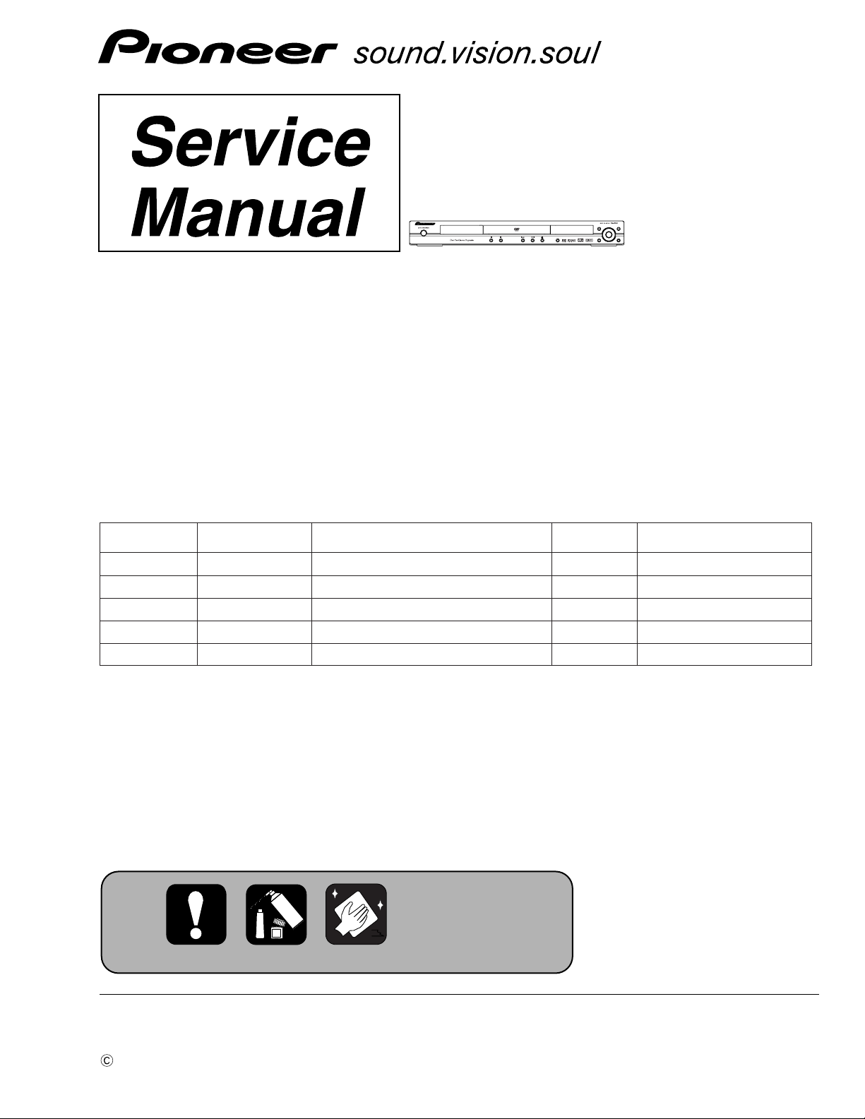
DV-393-S
DVD PLAYER
DV-393-S
DV-393-K
THIS MANUAL IS APPLICABLE TO THE FOLLOWING MODEL(S) AND TYPE(S).
Model Type Power Requirement Region No. Remarks
DV-393-S WYXZT5 AC220-240V 2
DV-393-S WVXZT5 AC220-240V 2
DV-393-S WYXZT/UR5 AC220-240V 5
DV-393-K WYXZT5 AC220-240V 2
DV-393-K WYXZT/UR5 AC220-240V 5
For details, refer to "Important Check Points for Good Servicing" .
T-ZZR MAR. 2006 printed in Japan
1234
SAFETY INFORMATION
A
This service manual is intended for qualified service technicians ; it is not meant for the casual doit-yourselfer. Qualified technicians have the necessary test equipment and tools, and have been
trainedto properly and safely repair complex products such as those covered by this manual.
Improperly performed repairs can adversely affect the safety and reliability of the product and
may void the warranty. If you are not qualified to perform the repair of this product properly and
safely, you should not risk trying to do so and refer the repair to a qualified service technician.
WARNING !
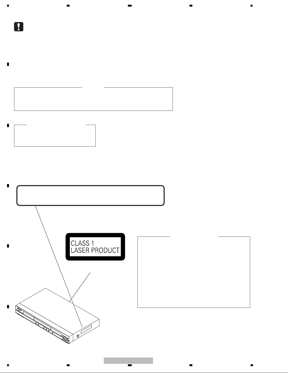
THE AEL (ACCESSIBLE EMISSION LEVEL) OF THE LASER POWER OUTPUT IS LESS THAN CLASS 1
B
BUT THE LASER COMPONENT IS CAPABLE OF EMITTING RADIATION EXCEEDING THE LIMIT FOR
CLASS 1.
A SPECIALLY INSTRUCTED PERSON SHOULD DO SERVICING OPERATION OF THE APPARATUS.
LASER DIODE CHARACTERISTICS
FOR DVD : MAXIMUM OUTPUT POWER : 5 mW
FOR CD : MAXIMUM OUTPUT POWER : 5 mW
WAVELENGTH : 650 nm
WAVELENGTH : 780 nm
C
LABEL CHECK
Location: inside of the unit
: VISIBLE AND INVISIBLE LASER RADIATION WHEN OPEN. AVOID EXPOSURE TO BEAM.
: SICHTBARE UND UNSICHTBARE LASERSTRAHLUNG,WENNABDECKUNG GEÖFFNET NICHT DEM STRAHL AUSSETZEN !
: SYNLIG OG USYNLIG LASERSTRÅLING VED ÅBNING UNDGÅ UDSÆTTELSE FOR STRÀLING.
: SYNLIG OCH OSYNLIG LASERSTRÅLNING NÄR DENNA DEL ÄR ÖPPNAD BETRAKTA EJ STRÅLEN.
: AVATTAESSA ALTISTUT NÄKYVÄ JA NÄKYMÄTTÖMÄLLE LASERSATEIL YLLE. ÄLÄ KATSO SÄTEESEN.
: RADIACIÓN LÁSER VISIBLE E INVISIBLE AL ESTAR ABIERTO. EVITAR EXPOSICIÓN AL RAYO.
D
E
CAUTION
VORSICHT
ADVARSEL
VARNING
VARO!
CUIDADO
(Printed on the Rear Panel)
7260000356 SH
Additional Laser Caution
1.
• Laser diode is driving with Q2303,Q2305(650nm LD) and Q2302,
Q2304(780nm LD)on the DVD MT PCB Assy.
Therefore, when short-circuit between the emitter and collector of these
transistors or the base voltage is supplied for transistors turn on, the
laser oscillates. (failure mode)
• In the test mode ∗ , there is the mode that the laser oscillates except
for the disc judgment and playback. LD ON mode in the test mode
oscillates with the laser forcibly.
2. When the cover is open, close viewing through the objective lens with
the naked eye will cause exposure to the laser beam.
∗ : See page 50.
F
2
DV-393-S
1234
5678
[Important Check Points for Good Servicing]
In this manual, procedures that must be performed during repairs are marked with the below symbol.
Please be sure to confirm and follow these procedures.
1. Product safety
Please conform to product regulations (such as safety and radiation regulations), and maintain a safe servicing environment by
following the safety instructions described in this manual.
1 Use specified parts for repair.
Use genuine parts. Be sure to use important parts for safety.
2 Do not perform modifications without proper instructions.
Please follow the specified safety methods when modification(addition/change of parts) is required due to interferences such as
radio/TV interference and foreign noise.
3 Make sure the soldering of repaired locations is properly performed.
When you solder while repairing, please be sure that there are no cold solder and other debris.
Soldering should be finished with the proper quantity. (Refer to the example)
4 Make sure the screws are tightly fastened.
Please be sure that all screws are fastened, and that there are no loose screws.
5 Make sure each connectors are correctly inserted.
Please be sure that all connectors are inserted, and that there are no imperfect insertion.
6 Make sure the wiring cables are set to their original state.
Please replace the wiring and cables to the original state after repairs.
In addition, be sure that there are no pinched wires, etc.
7 Make sure screws and soldering scraps do not remain inside the product.
Please check that neither solder debris nor screws remain inside the product.
8 There should be no semi-broken wires, scratches, melting, etc. on the coating of the power cord.
Damaged power cords may lead to fire accidents, so please be sure that there are no damages.
If you find a damaged power cord, please exchange it with a suitable one.
9 There should be no spark traces or similar marks on the power plug.
When spark traces or similar marks are found on the power supply plug, please check the connection and advise on secure
connections and suitable usage. Please exchange the power cord if necessary.
0 Safe environment should be secured during servicing.
When you perform repairs, please pay attention to static electricity, furniture, household articles, etc. in order to prevent injuries.
Please pay attention to your surroundings and repair safely.
A
B
C
D
2. Adjustments
To keep the original performance of the products, optimum adjustments and confirmation of characteristics within specification.
Adjustments should be performed in accordance with the procedures/instructions described in this manual.
3. Lubricants, Glues, and Replacement parts
Use grease and adhesives that are equal to the specified substance.
Make sure the proper amount is applied.
4. Cleaning
For parts that require cleaning, such as optical pickups, tape deck heads, lenses and mirrors used in projection monitors, proper
cleaning should be performed to restore their performances.
5. Shipping mode and Shipping screws
To protect products from damages or failures during transit, the shipping mode should be set or the shipping screws should be
installed before shipment. Please be sure to follow this method especially if it is specified in this manual.
56
DV-393-S
E
F
3
7
8

1234
CONTENTS
SAFETY INFORMATION ..................................................................................................................................... 2
1. SPECIFCATIONS ............................................................................................................................................. 5
2. EXPLODED VIEWS AND PARTS LIST ............................................................................................................ 6
A
B
C
D
2.1 PACKING SECTION .................................................................................................................................. 6
2.2 EXTERIOR SECTION................................................................................................................................ 8
2.3 06 DVD MECHA SECTION...................................................................................................................... 10
3. BLOCK DIAGRAM AND SCHEMATIC DIAGRAM..........................................................................................12
3.1 BLOCK DIAGRAM ................................................................................................................................... 12
3.2 POWER BLOCK DIAGRAM..................................................................................................................... 13
3.3 OVERALL WIRING CONNECTION DIAGRAM........................................................................................ 14
3.4 DVD MT PCB ASSY (1/6)........................................................................................................................ 16
3.5 DVD MT PCB ASSY(2/6)......................................................................................................................... 18
3.6 DVD MT PCB ASSY(3/6)......................................................................................................................... 20
3.7 DVD MT PCB ASSY(4/6)......................................................................................................................... 22
3.8 DVD MT PCB ASSY(5/6)......................................................................................................................... 24
3.9 DVD MT PCB ASSY(6/6)......................................................................................................................... 26
3.10 OPERATION 1, OPERATION 2 and OPERATION 3 PCB ASSYS ........................................................ 28
3.11 POWER PCB ASSY (1/2) ...................................................................................................................... 30
3.12 POWER PCB ASSY (2/2) ...................................................................................................................... 32
3.13 WAVE FORMS....................................................................................................................................... 34
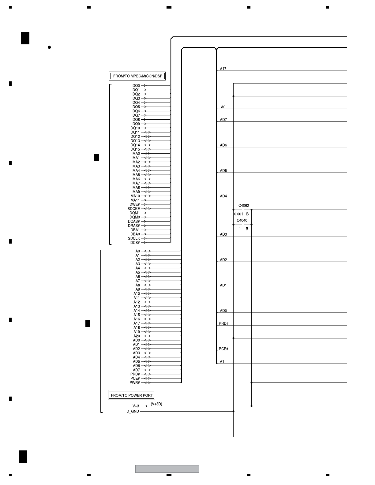
4. PCB CONNECTION DIAGRAM ..................................................................................................................... 37
4.1 LOADING and SW PCB ASSYS.............................................................................................................. 37
4.2 DVD MT PCB ASSY................................................................................................................................. 38
4.3 OPERATION 1, OPERATION 2 and OPERATION 3 PCB ASSYS .......................................................... 42
4.4 POWER PCB ASSY................................................................................................................................. 46
5. PCB PARTS LIST ........................................................................................................................................... 48
6. ADJUSTMENT ............................................................................................................................................... 49
6.1 WHEN REPLACING DVD DECK ............................................................................................................. 49
6.2 TEST MODE ............................................................................................................................................ 50
6.3 TEST MODE IN........................................................................................................................................ 51
6.4 DISC REMOVAL METHOD...................................................................................................................... 52
7. GENERAL INFORMATION............................................................................................................................. 53
7.1 DIAGNOSIS ............................................................................................................................................. 53
7.1.1 DISPLAY SPECIFICATION OF THE TEST MODE............................................................................ 53
7.1.2 FUNCTIONAL SPECIFICATION OF THE SHORTCUT KEY ............................................................ 54
7.1.3 SPECIFICATION OF MODEL INFORMATION DISPLAY .................................................................. 55
7.1.4 FUNCTIONAL SPECIFICATION OF THE SERVICE MODE............................................................. 56
7.1.5 METHOD FOR DIAGNOSING DEGRADATION OF THE LDS ON THE PICKUP ASSY .................. 57
7.1.6 TROUBLE SHOOTING...................................................................................................................... 58
7.2 DISASSEMBLY ........................................................................................................................................ 61
7.3 DVD DECK SECTION.............................................................................................................................. 62
7.4 IC INFORMATION.................................................................................................................................... 66
7.5 DISC / CONTENT FORMAT PLAYBACK COMPATIBILITY ..................................................................... 78
8. PANEL FACILITIES ........................................................................................................................................ 80
8.1 FRONT PANEL SECTION ....................................................................................................................... 80
8.2 REMOTE CONTROL ............................................................................................................................... 81
E
F
4
1234
DV-393-S
5678
1. SPECIFCATIONS
Specifications
General
System . . . . . . . . . . . . . . . . . . . . . . DVD player
Power requirements . AC 220to240 V, 50/60 Hz
Power consumption . . . . . . . . . . . . . . . . . 7 W
Power consumption (standby) . . . . . . 0.7 W
Weight . . . . . . . . . . . . . . . . . . . . . . . . 1.7 kg
Dimensions:
DV-393 . . . . . 420 (W) x 49.5 (H) x 214 (D) mm
Operating temperature . . . . . . . +5°C to +35°C
Operating humidity . . . . . . . . . . . . . 5% to 85%
(no condensation)
Video output
Output level . . . . . . . . . . . . . . . 1 Vp-p (75Ω)
Jack . . . . . . . . . . . . . . . . . . . . . . . . . . . . . . RCA
Audio output (1 stereo pair)
Output level . . . . . . . . . . During audio output
200 mVrms (1 kHz, –20 dB)
Number of channels . . . . . . . . . . . . . . . . . . . 2
Jacks . . . . . . . . . . . . . . . . . . . . . . . . . . . . . RCA
A
B
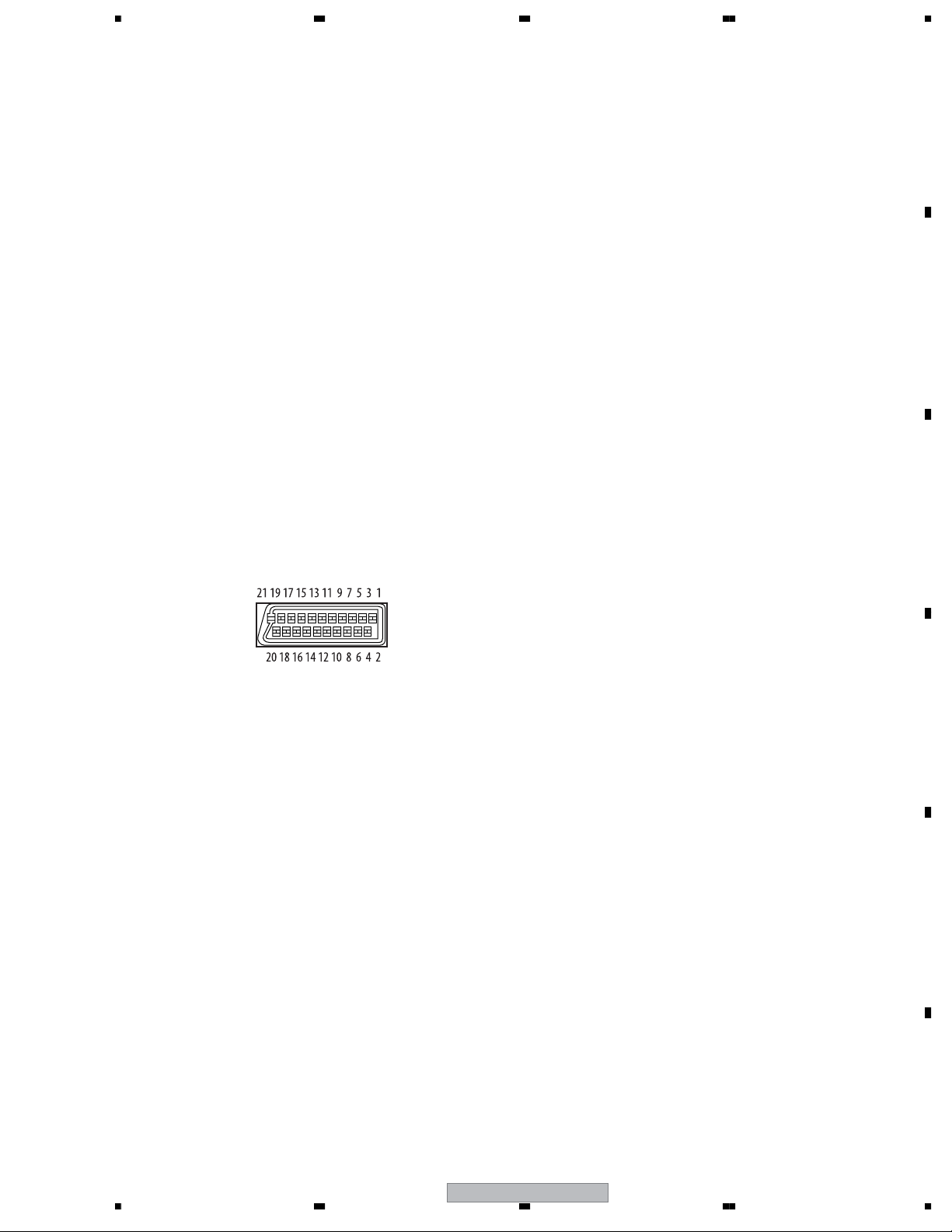
AV connector output
AV Connector (21-pin connector assignment)
AV connector output . . . . . . . 21-pin connector
This connector provides the video and audio
signals for connection to a compatible colour TV
or monitor.
PIN no.
1 . . . . . . . . . . . . . . . . . . . . . . . Audio 2/R out
3 . . . . . . . . . . . . . . . . . . . . . . . . . Audio 1/L out
4 . . . . . . . . . . . . . . . . . . . . . . . . . . . . . . . GND
7 . . . . . . . . . . . . . . . . . . . . . . . . . . . . . . . B out
8 . . . . . . . . . . . . . . . . . . . . . . . . . . . . . . Status
11 . . . . . . . . . . . . . . . . . . . . . . . . . . . . . . G out
15 . . . . . . . . . . . . . . . . . . . . . . . . . . . . . . R out
17 . . . . . . . . . . . . . . . . . . . . . . . . . . . . . . GND
19 . . . . . . . . . . . . . . . . . . . . . . . . . . . Video out
21 . . . . . . . . . . . . . . . . . . . . . . . . . . . . . . GND
Component video output
Y (luminance) - Output level . . . 1 Vp-p (75 Ω )
P
B (color) - Output level . . . . 0.7 Vp-p (75Ω )
P
R (color) - Output level . . . . . 0.7 Vp-p (75 Ω)
Jack . . . . . . . . . . . . . . . . . . . . . . . . . . . . . . RCA
Digital audio characteristics
Frequency response . . . . . . . . 4 Hz to 44 kHz
(DVD fs: 96 kHz)
S/N ratio . . . . . . . . . . . . . . . . . . . . . . . . . 115 dB
Dynamic range . . . . . . . . . . . . . . . . . . . . 88 dB
Total harmonic distortion . . . . . . . . . . 0.0065 %
Wow and flutter . . . . . . Limit of measurement
(±0.001% W. PEAK) or lower
Digital output
Coaxial digital output . . . . . . . . . . . . . RCA jack
Accessories
Audio/video cable. . . . . . . . . . . . . . . . . . . . . . . . 1
Power cable. . . . . . . . . . . . . . . . . . . . . . . . . . . . . 1
Remote control. . . . . . . . . . . . . . . . . . . . . . . . . . 1
AA/R6P dry cell batteries . . . . . . . . . . . . . . . . . 2
Warranty card. . . . . . . . . . . . . . . . . . . . . . . . . . . 1
Operating Instructions
The specifications and design of this product are subject to
change without notice, due to improvement.
Published by Pioneer Corporation.
Copyright © 2006 Pioneer Corporation.
All rights reserved
C
D
E
56
DV-393-S
F
5
7
8
1234
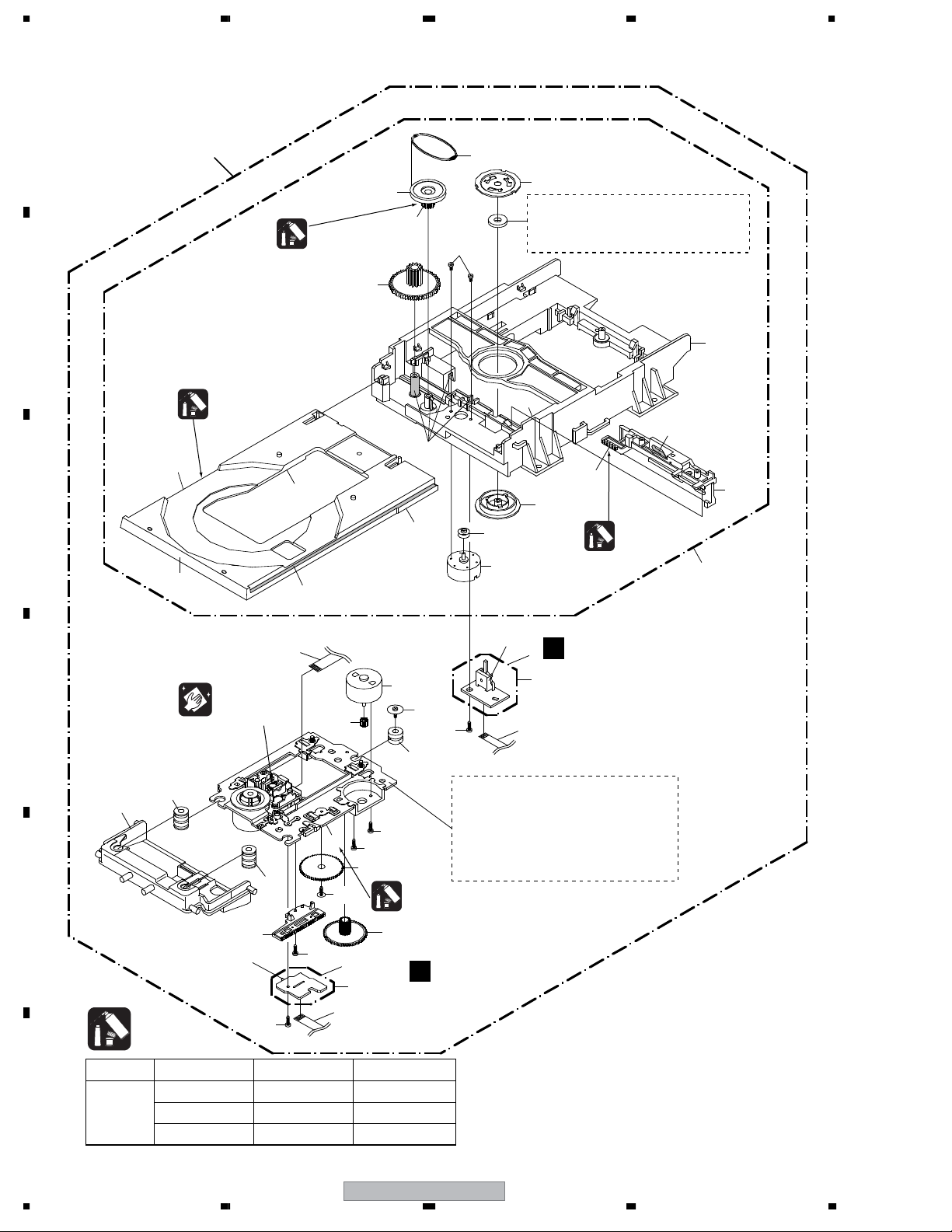
2. EXPLODED VIEWS AND PARTS LIST
NOTES:
Parts marked by "NSP" are generally unavailable because they are not in our Master Spare Parts List.
The mark found on some component parts indicates the importance of the safety factor of the part.
A
Therefore, when replacing, be sure to use parts of identical designation.
Screws adjacent to mark on product are used for disassembly.
For the applying amount of lubricants or glue, follow the instructions in this manual.
(In the case of no amount instructions, apply as you think it appropriate.)
2.1 PACKING SECTION
GUARANTEE CARD
INSTRUCTION BOOK (E)
INSTRUCTION BOOK (E/I)
B
INSTRUCTION BOOK (G/F)
INSTRUCTION BOOK (S/H)
INSTRUCTION BOOK (R)
7-10,17
"Operating Instructions"
5
C
BATTERY,MANGAN
6
7
8
9
10
17
POLYBAG,INSTRUCTION (RED CAUTION)
12
14
POLY BAG INSTA5
TRANSMITTER
CORD,RCA PIN
16
PA CKAGE
For WVXTL type
2
1
For WYXZT5, WYXZT/UR5 types
3
4
2
1
PA CKAGE
14
GIFT SHEET
13
Front
D
PA CKAGE
14
E
11
PA CKAGE,PAD
PA CKAGE
14
15
F
6
1234
DV-393-S
>
>
5678
PACKING SECTION parts List
No. Description Part No.
Mark
1 Cord Set AC See Contrast table (2)
2 Cord, RCA Pin 06CPBA2006
3 Remote Control 07650KY040
4 Battery Cover VNK4998
NSP 5 Battery,Mangan (AR, R6P) 141L003010
NSP 6 Guarantee Card J2I80202A
7 Instruction Book See Contrast table (2)
8 Instruction Book See Contrast table (2)
9 Instruction Book See Contrast table (2)
10 Instruction Book See Contrast table (2)
No. Description Part No.
Mark
11 Package.Pad 792WHA0604
12 Polyethylene Bag,Instruction JB5UD400
13 Gift Sheet 791WHA0100
14 Package See Contrast table (2)
15 Gift Box See Contrast table (2)
16 Poly. Bag 791WHAA040
17 Instruction Book See Contrast table (2)
A
(2) CONTRAST TABLE
DV-393-S/WVXT5, /WYXZT/UR5, DV-393-K/WYXZT5, /WYXZT/UR5 and DV-393-S/WYXZT5 are constructed the
same except for the following :
Mark No. Symbol and Description
1 Cord Set AC 1206158802 1206138802 1206158802 1206158802 1206158802
7 Instruction Book (English) Not used J2I80601B Not used Not used Not used
8 Instruction Book (English, Italian) J2I80221B Not used Not used J2I80221B Not used
9 Instruction Book (German, French) J2I80222B Not used Not used J2I80222B Not used
10 Instruction Book (Spanish, Duch) J2I80223B Not used Not used J2I80223B Not used
14 Package 792WHAA190 792WHAA191 792WHAA190 792WHAA190 792WHAA190
15 Gift Box 793WCD1734 793WCDD120 793WCD1734 793WCDD125 793WCDD125
17 Instruction Book (Russian) Not used Not used J2I80801B Not used J2I80801B
DV-393-S/
WYXZT5
DV-393-S/
WVXZT5
DV-393-S/
WYXZT/UR5
DV-393-K/
WYXZT5
DV-393-K/
WYXZT/UR5
B
C
D
56
DV-393-S
E
F
7
7
8
1234
2.2 EXTERIOR SECTION
NON-CONTACT
A
SIDE
CONTACT SIDE
Refer to
"2.3 06 DVD MECHA ASSY".
20
14
20
5
18
17
20
18
PCB240
(POWER PCB ASS'Y)
B
19
19
4
19
6
F
19
11
C
13
18
16
16
18
21
25
10
12
21
12
24
23
19
20
21
19
20
19
D
E
101E
101C
101
" FRONT PANEL SECTION".
F
101M
101G
PCBDF0
(OPERATION 3 PCB ASS'Y)
27
22
G
101N
101D
101I
101A
8
13
PCB280
(OPERATION 2 PCB ASS'Y)
22
3
C
101J
101B
101H
101F
101K
101L
22
22
26
A
1
PCB130
(DVD PCB ASS'Y)
22
B
PCB270
(OPERATION 1 PCB ASS'Y)
22
2
19
8
1234
DV-393-S
>
5678
EXTERIOR SECTION parts List
No. Description Part No.
Mark
1DVD MT PCB Assy A2I802A130
2 OPERATION 1 PCB Assy A2I802A270
3 OPERATION 2 PCB Assy A2I802A280
4POWER PCB Assy A2I802A240
5DVD MECHA ASSY A2I802A650
6 Shield,21Pin 761WSA0237
7• • • •
NSP 8 Plate,Bottom 702WSA0283
9• • • •
NSP 10 Sheet,Caution 726000A140
11 Plate,Cover power 755WPAA031
12 Holder,FFC 761WPA0396
13 Cushion,Leg VEB1349
14 Cabinet,Top See Contrast table (2)
15 • • • •
16 Cushion (15x20x16) 8965TS1015
NSP 17 POP Label 7236310030
18 Screw,Tap Tite(S)-Bind Wash. 816423063U
19 Screw,Tap Tite(S) (3x5.5) 8107D3055U
20 Screw,Tap Tite(B) (3x6.0) See Contrast table (2)
21 Screw,Tap Tite(B)Pan (3x6) 810913060U
22 Screw,Tap Tite(P) (2.6x8) 811022680U
No. Description Part No.
Mark
NSP 23 Sheet,Jack 1 7226310105
NSP 24 Sheet,Jack 2 See Contrast table (2)
NSP 25 Sheet,Jack 3 See Contrast table (2)
NSP 26 Double,Face-Tape 7290000156
27 OPERATION 3 PCB Assy A2I802ADF0
101 Front Cabi Assy See Contrast table (2)
NSP 101A Cabinet,Front See Contrast table (2)
NSP 101B Plate, Display 711WPA0253
NSP101C Plate, Cover 711WPD0696
101D Flap,DVD 712WPD0184
NSP101E Badge,Brand See Contrast table (2)
NSP 101F Button,Frame 1 735WPA0874
NSP101G Button,Frame 4 735WPA0879
NSP 101H Button,Frame 2 See Contrast table (2)
NSP 101I Button,Frame 5 See Contrast table (2)
NSP 101J Button,Frame 3 See Contrast table (2)
NSP 101K Button, Cap See Contrast table (2)
NSP101L Button, Cap 2 See Contrast table (2)
NSP 101MButton, Cap 1 See Contrast table (2)
101N Spring,Flap-DVD 743WKA0052
A
B
C
(2) CONTRAST TABLE
DV-393-S/WVXT5, /WYXZT/UR5, DV-393-K/WYXZT5, /WYXZT/UR5 and DV-393-S/WYXZT5 are constructed the
same except for the following :
Mark No. Symbol and Description
14 Cabinet, Top 702WSB0114 702WSB0114 702WSB0114 702WSB0115 702WSB0115
20 Screw,Tap Tite(B) (3x6.0) 8109K3060U 8109K3060U 8109K3060U 8109K3060S 8109K3060S
NSP 24 Sheet, Jack 2 7226310106 7226310106 7226310106 722631A074 722631A074
NSP 25 Sheet, Jack 3 7226310107 7226310107 722631A075 722631A076 722631A077
101 Front Cabi Assy 7A7010195A 7A7010195A 7A7010195A 7A701A684A 7A701A684A
NSP 101A Cabinet, Front 701WPJ1416 701WPJ1416 701WPJ1416 701WPJD263 701WPJD263
NSP 101E Badge, Brand 7236310014 7236310014 7236310014 7236310009 7236310009
NSP 101H Button, Frame 2 735WPB0328 735WPB0328 735WPB0328 735WPA0876 735WPA0876
NSP 101I Button, Frame 5 735WPB0329 735WPB0329 735WPB0329 735WPA0881 735WPA0881
NSP 101J Button, Frame 3 735WPB0330 735WPB0330 735WPB0330 735WPA0878 735WPA0878
NSP 101K Button, Cap 737WPB0005 737WPB0005 737WPB0005 737WPA0037 737WPA0037
NSP 101L Button, Cap 2 737WPB0006 737WPB0006 737WPB0006 737WPA0040 737WPA0040
NSP 101M Button, Cap 1 737WPJ0002 737WPJ0002 737WPJ0002 737WPDA001 737WPDA001
DV-393-S/
WYXZT5
DV-393-S/
WVXZT5
DV-393-S/
WYXZT/UR5
DV-393-K/
WYXZT5
DV-393-K/
WYXZT/UR5
D
E
56
DV-393-S
F
9
7
8
1234
2.3 06 DVD MECHA SECTION
A
34
14
9
18
Cannot supply separately.
Lubricating Oil
GYA1001
AB
21
If the repair is needed, replace the
LOADER SUB ASS'Y.
15
B
11
Daifree
GEM1036
AB
AB
AB
AC
AB
C
AB
4
20
3
12
AC
AB
Lubricating Oil
GYA1001
23
19
29
6
CD2001
SW1
E
1
PCB610
Pickup leneses
D
8
13
E
GEM1004
GED-008
25
30
24
AA
8
26
27
17
SW2
Note :
5
32
31
10
22
22
16
Grease
GEM1018
2
PCB640
D
(SW PCB ASS'Y)
Do not replace the parts. Because,
minute adjustments are needed if
this condition is disassembled
further more.
If the repair is needed, replace the
DVD MECHA ASS'Y.
(LOADING MOTOR PCB ASS'Y)
7
CD2302
28
33
CLASS
GREASE G-555G
F
PART NO.
GEM1018
GYA1001
PART NAME
GEM1036
G-313Y
FL-78A
CD2301
MARK
AA
AB
AC
NOTE:
Applying positions AA, AB and AC for the
grease are displayed for this section.
Check if the correct grease is applied for each
position.
10
DV-393-S
1234

5678
06 DVD MECHA SECTION parts List
No. Description Part No.
Mark
1 Loading Motor PCB Assy A2F101A610
2 Gear,Middle 92P100117A
3 Loading Motor 1515S98004
4 Pulley,Motor 92P100097A
5 FEED Motor 1515S98004
6 Cord Jumper (24P)(CD2001) 122J402202
7 Cord Jumper (CD2302) 122H051602
8 Insulator (F) 92P200013A
9 Belt,Loading 92P200015A
10 Insulator (R) 92P200016A
A
11 Frame,main 92P100119A
12 Tray (B) 92P100127B
13 Holder ,Traverse 92P100125A
14 Gear,Pulley 92P100123A
15 Gear,Main 92P100124A
16 Gear,Feed 92P100116A
17 SW PCB Assy (PCB640) A2F101A640
18 Plate, Clamper 92P000023A
19 LOADER SUB ASSY (B) 92AAA0019B
20 Clamper 92P100122A
21 Screw,Pan (M1.7x3 P3) 814011730U
22 Screw,Pan (M1.7x2.3 P3) 814011723U
23 Rack,Loading 92P100121A
24 Gear,Motor 92P100088A
25 Feed Rack Assy 92AAA0017A
26 Screw,T-Tite(B) (M1.7x5.0 P3) 813381750U
27 Screw,Gear Feed 92P700007A
28 Cord Jumper (CD2301) 122H061605
29 Switch (SW1) 0515S32003
30 Push Switch (SW2) 0500101036
31 Screw,Tap Tite(P) (2.6x8) 811022680U
32 Sems.Tap Tite(P) (2x8) 816112080U
33 Screw (Bind 2x8) 811022080U
34 DVD MECHA ASSY A2I802A650
B
C
D
56
DV-393-S
E
F
11
7
8
1234
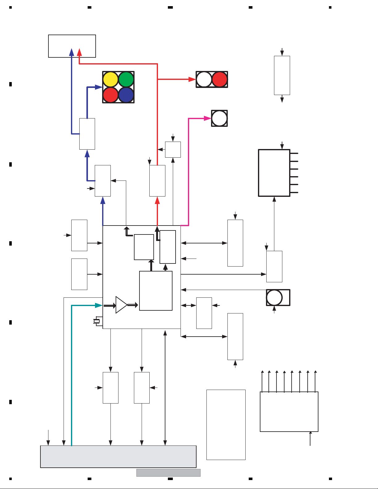
3. BLOCK DIAGRAM AND SCHEMATIC DIAGRAM
3.1 BLOCK DIAGRAM
A
SCART
L/R
R, G, B
(21Pin/D-Connector Block)
B
• DV-393-S / MPEG / FIP Block Diagram
Y
CVBS
V
Y, CB, CR,
IC7302
BUS SW
SN74CBT325
C
CVBS
IC7301
LA73054
Video Driver
U
RCA-405A-08
Video Jack (J7302)
AMP_AUDIO_L/R
F
IC8003
MUTE
RC4580
Audio AMP
E
L
R
RCA-207B-02
Audio Jack (J8003)
Coa
Coaxial
(J8001)
RCA-117-01
,
,
A
IC4006
+1.8V REG
LM1117S-ADJ
B
G
FIP (V651)
8-BT-234GNK
C
4ch VID EO
Reset IC
BD5229 G-TR
X4001
27MHz X'tal
27MHz
/URST
IC4001
IC4003
A
D
I/XP, LETTER, SQUEEZE
108MHz
MT1389E
MPEG/u-CON Block
RF AMP
MPEG-1/2/
AUDIO_L/R
TV Encoder
Audio CODEC
JPEG
Video Decorder
/Internal DAC
I2C
DQ1 ~ DQ15,
MA1 ~ MA11,
/DWE, DBA0, DBA1
/DCS, /DRAS, /DCAS
SDCLK, SDCKE, DDQM0
A, B
IC4002
BR24L08FJ
8K EEPROM
IC4005
64Mbit SDRAM
EM638165TS-7G
A
GR1 ~ GR8,
P1 ~ P16
A
DI, DO, SCK, STB
IC651
PT6315
FIP Driver
IR
IR
ROM-N340TAO
A
IR Receiver (OS651)
IC4004
V1R4
E
IOA, V20
RF, A, B, C, D, E, F, MD I
LDO1, LDO2
A
C
F
U
DVD
Loader
(DM-4)
OP
12
DMSO, FMSO,
TROPEN, TRCLO
TRSO, FOSO, STB
LD Driver
Q2302 ~ 2305
MOT_LD+/-,
TR+/-, FO+ /-,
LD_DVD, LD_CD
(06SD)
MOT_SLED+/-,
D
IC2301
LA6565VR
Motor Driver
MOT_SPDL+/-
SLED
MOTOR
SPINDLE
STEPING
DV-393-S
OPO, OP+/-
LIMIT, TRIN, TROUT,
A0 ~ A20,
AD0 ~ AD7,
A • • • • AT+3.3V
B • • • • +1.8V
16Mbit(1Mx16)Flash
S29AL016D70TFI020
A A
/PRD, /PCE, /PWR
C • • • • P.CON+5V
D • • • • P.CON+6V
E • • • • AT+12V
F • • • • P.CON+12V
G • • • • -28V
P.CON+12V
P.CON+6V
P.CON+5V
POWER
SUPPLY
AT+3.3V
AT+3.3V
FLDC +/-
AT+12V for mute
-28V
AC220V-240V
1234
5678
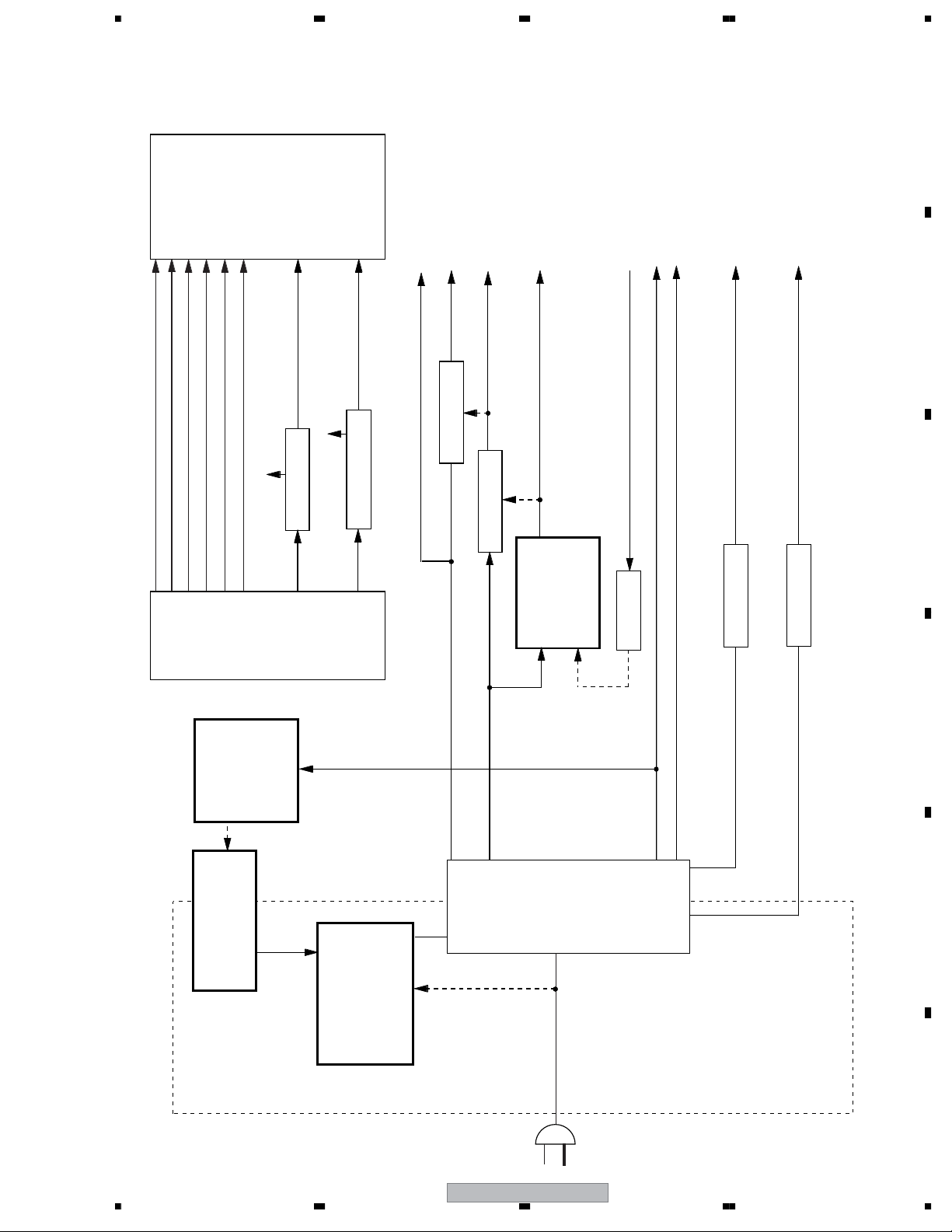
3.2 POWER BLOCK DIAGRAM
• POWER/21 PIN BLOCK DIAGRAM
J8101
R_VIDEO
G_VIDEO
B_VIDEO
21PIN CONNECTOR
21 PIN CTL
P.CON +12V
21 PIN CTL
Q8102
AUDIO_L
CVBS_VIDEO
AUDIO_R
BLANKING_OUT
AT+3.3V
DVD_RGB_H_OUT
Q8104, Q8105
AT+12V for mute
P.CON+5V
P.CON+12V
P.CON +12V SW
Q510
Q515
P.CON+6V
P.CON +5V SW
AT+3.3V
P.CON-H
FL DC -
FL DC +
A
-28V
B
C
CP503
(CP8001)
VOLTAGE CTL
IC504
PHOTO COUPLER
PS2561AL1-1-V (W)
FFC
IC501
KIA431A-AT
P-H/I-L
ASP/FS
CONNECTOR
_RGB-H
IC502
POWER CTL
STR-A6151M
IC503
6V REG
PQ070XF01SZH
T501
TRANS
SWITCHING
P.CON SW
Q505
FL + P.CON SW
Q504
-28V P.CON SW
Q502
D
E
AC IN
DV-393-S
56
F
13
7
8
1234
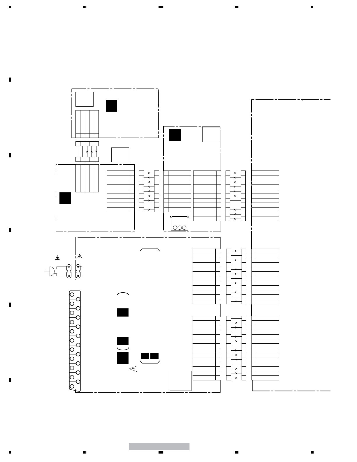
3.3 OVERALL WIRING CONNECTION DIAGRAM
A
DEF086
PCBDF0
OPE3 PCB
G
B
V+3E
GND(NC)
CD604(5P FFC)
122H051706
(CD604)
54321
GND(NC)
V+3E
C
C
OPERATION 2
PCB ASSY
(A2I802A280)
CD507_8
AC230V-240V_50Hz
D
AC IN
E
J501
21PIN CONNECTOR
J8101
1
NC
5
NC
7
9
NC
11
NC
13
15
17
19
NC
21 3
12
NN
220
4
6
8
10
12
14
16
18
SCART
L
OPERATION 3
LED
SW2
POWER
PCB ASSY
(A2I802ADF0)
54321
CP605
54321
56789
CP604
SW2
LED
POWER
PLAY/+SKIP
PAUSE/-SKIP
OPE2 PCB
PCB280
DEF085
CP603
SW1
STOP
V+3E
POWER
SW2
GND
LED
B
OPERATION 1
CD602
(9P FFC)
122H091303
(CD602)
9
9
8
8
7
7
6
6
5
5
4
4
3
3
2
2
1
1
(CD602)
F 1/2, F 2/2
F
: POWER BLOCK
F 1/2
POWER PCB ASSY (A2I802A240)
PCB ASSY
(A2I802A270)
CP602
1
1
2
3
4
5
6
7
8
9
2
3
4
5
6
7
8
9
OS651
SW1
STOP
PLAY/+SKIP
PAUSE/-SKIP
V+3E
POWER
SW2
GND
LED
: 21PIN/D/DIGITAL AUDIO BLOCK
F 2/2
POWER PCB
PCB024
DPF010
VoutB+GND
123
AT+12V for MUTE
OPE1 PCB
PCB270
DEF084
CP601
CLK
DI (M to F)
STB
DO (F to M)
IR
V+3E
DGND
DGND
FLDC+
-28V
FLDC-
CP503
G/Y
GND
B/CB
GND
R/CR
RGB-H
FS
CVBS
GND
AUDIO L
GND
AUDIO R
CP502
GND
P.CON+12V
GND
P.CON+5V
P.CON+6V
GND(M)
AT+3.3V
P.ON-H
GND(D)
FL DCFL DC+
-28V
CD601
(11P FFC)
122H0B1003
1
1
2
2
3
3
4
4
5
5
6
6
7
7
8
8
9
9
10
10
11
11
(CD601)
CD7301
(12P FFC)
122HC0C3002
12
12
11
11
10
10
9
9
8
8
7
7
6
6
5
5
4
4
3
3
2
2
1
112
(CD502)
1
1
2
2
3
3
4
4
5
5
6
6
7
7
8
8
9
9
10
10
11
11
12
12
13
13
14
14
CP502(14P)
Cord Connector
CU3E3001
1
2
3
4
5
6
7
8
9
10
11
1
2
3
4
5
6
7
8
9
10
11
1
2
3
4
5
6
7
8
9
10
11
12
13
14
CP4002
CLK
1
2
DI (M to F)
3
STB
4
DO (F to M)
5
6
V+3E
7
DGND
8
DGND
9
FLDC+
10
-28V
11
FLDC-
CP7301
G/Y
1
GND
2
B/CB
3
GND
4
R/CR
5
RGB-H
6
7
CVBS
8
GND
9
AUDIO L
10
GND
11
AUDIO R
12
CP4003
GND
1
P.CON+12V
2
AT+12V for MUTE
3
GND
4
P.CON+5V
5
P.CON+6V
6
GND(M)
7
AT+3.3VAT+3.3V
8
AT+3.3V
9
P.ON-H
10
GND(D)
11
FL DC-
12
FL DC+
13
-28V
14
IR
FS
F
14
DV-393-S
1234
5678
÷
When ordering service parts, be sure to refer to "EXPLODED VIEWS and PARTS LIST" or
"PCB PARTS LIST".
÷
The > mark found on some component parts indicates the importance of the safety factor
A
of the part. Therefore, when replacing, be sure to use parts of identical designation.
÷
DIGITAL OUT
H
2
1
E
COAXIAL
J8001
RCA-117-01
A
DVD PCB
PCB130
DMF072
A 1/6- A 6/6
AUDIO OUT
H1H2
23
1
E
DVD AUDIO OUT
J8003
RCA-207B-02
DVD MT PCB ASSY (A2I802A130)
: MPEG/MICON/RF-AMP BLOCK
A 1/6
: MEMORY BLOCK
A 2/6
: LOADER/MOTOR DRV BLOCK
A 3/6
: AUDIO JACK BLOCK
A 4/6
: VIDEO JACK BLOCK
A 5/6
: POWER PORT BLOCK
A 6/6
: The power supply is shown with the marked box.
VIDEO OUT
(COMPOSITE)
H1H2EH1H2
23
56
1
4
E
CVBS/Y/U/V
J7302
RCA-405A-08
CP2301
24
F RTN
F DRV
T RTN
T DRV
NC
GND
LD(DVD)
PD/GND
LD(CD)
GND
VR(CD)
VR COM
VR(DVD)
A
B
VRF(RF_OUT)
SW1(DVD/CD)
C
D
E
VCC
VS
F
GND
CP2303
SP1+
SP1SLD+
SLD-
LIMIT SW
SW(GND)
24
23
23
22
22
21
21
20
20
19
19
18
18
17
17
16
16
15
15
14
14
13
13
12
12
11
11
10
10
9
9
8
8
7
7
6
6
5
5
4
4
3
3
2
2
1
1
1
1
2
2
3
3
4
4
5
5
6
6
CP2302
CLOSE
1
GND(D)
2
OPEN
3
4
LD- LD-
5
DVD MECHA ASSY
(A2I802A650)
F RTN
24
F DRV
23
T RTN
22
T DRV
21
20
19
18
17
16
15
14
13
12
11
10
9
8
7
6
5
4
3
2
1
1
2
3
4
5
6
CD2302
NC
GND
LD(DVD)
PD/GND
LD(CD)
GND
VR(CD)
VR COM
VR(DVD)
A
B
VRF(RF_OUT)
SW1(DVD/CD)
C
D
E
VCC
VS
F
GND
SW PCB ASSY
D
(A2F101A640)
CD2301
SP1+
SP1SLD+
SLD-
LIMIT SW
SW(GND)
LOADING MOTOR
E
PCB ASSY
M
M
ESE22MH22
(A2F101A610)
SW-2(CLOSE)
GND(SW)
SW-1(OPEN)
LD+LD+
LOADING MOTOR
M
DVD
DRIVE
DM-4PB
OPTICAL PICK-UP
M2601
JCV9B12
SPINDLE MOTOR
M2602
BCZ3B05
SLED MOTOR
SW2
SW1
SSS-28-5
M2603
BCZ3B05
B
C
D
E
56
DV-393-S
F
D E
15
7
8
1234
3.4 DVD MT PCB ASSY (1/6)
A
B
C
A 1/6
FROM/TO
LOADER/MOTOR DRV
(RF)
FROM/TO MEMORY
DVD MT PCB ASSY (A2I802A130)
MPEG/MICON/RF-AMP BLOCK
(D)
(A)
(B)
(C)
(RF)
(E)
(F)
(RF)
(E)
(F)
(D)
(A)
(B)
(C)
D
2/6A 3/6A
E
F
7
8
EEPROM
A 1/6
16
DV-393-S
1234
5678
(RF)
: RF SIGNAL ROUTE
: VIDEO SIGNAL ROUTE
(SY)
: S VIDEO SIGNAL ROUTE (Y ch)
(SC)
: S VIDEO SIGNAL ROUTE (C ch)
(R/CR)
: VIDEO SIGNAL ROUTE (R/CR ch)
(G/Y)
: VIDEO SIGNAL ROUTE (G/Y ch)
(B/CB)
: VIDEO SIGNAL ROUTE (B/CB ch)
(D)
: AUDIO DATA SIGNAL ROUTE
(DA)
: AUDIO SIGNAL ROUTE (Digital)
NOTE:THE DC VOLTAGE EACH PART WAS
MEASURED WITH THE DIGITAL TESTER
DURING PLAYBACK.
(R/CR)
(B/CB)
(G/Y)
3
NOTE:THIS SCHEMATIC DIAGRAM IS THE LATEST AT THE TIME
OF PRINTING AND SUBJECT TO CHANGE WITHOUT NOTICE
6/6A
(R/CR)
(B/CB)
(G/Y)
5/6A
4/6A
2
A
B
C
D
RESET IC
DV-393-S
56
CP601
B
6
E
F
A 1/6
17
7
8
1234
3.5 DVD MT PCB ASSY(2/6)
A
B
C
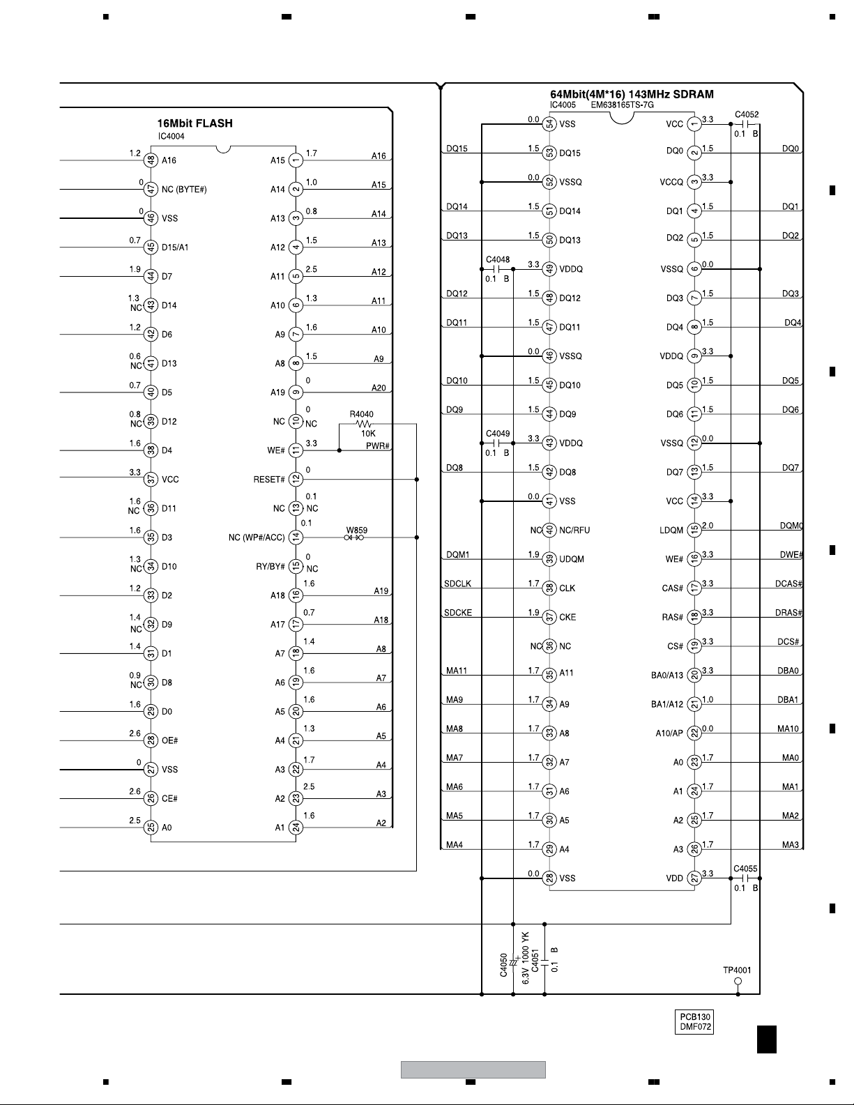
A 2/6
DVD MT PCB ASSY (A2I802A130)
MEMORY BLOCK
1/6A
D
1/6A
E
F
A 2/6
18
DV-393-S
1234
5678
A
S29AL016D70TFI020
B
C
D
E
NOTE :THIS SCHEMATIC DIAGRAM IS THE LATEST AT THE TIME
OF PRINTING AND SUBJECT TO CHANGE WITHOUT NOTICE
56
NOTE : THE DC VOLTAGE EACH PART WAS
MEASURED WITH THE DIGITAL TESTER
DURING PLAYBACK.
DV-393-S
7
F
A 2/6
19
8
1234
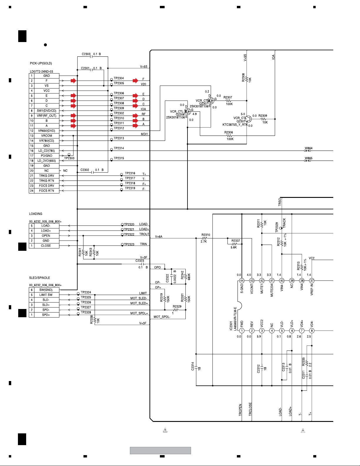
3.6 DVD MT PCB ASSY(3/6)
A
B
C
A 3/6
CP2301
To PICKUP
DVD MT PCB ASSY (A2I802A130)
LOADER/MOTOR DRIVE BLOCK
(F)
(E)
(D)
(C)
(RF)
(B)
(A)
(F)
(E)
(D)
(C)
(RF)
(B)
(A)
D
E
CP2302
CD2302
D
CP2303
CD2301
E
MOTOR DRIVER
F
20
A 3/6
ATTENTION
: LES PIECES REPAREES PAR UN ETANT
DANGEREUSES AN POINT DE VUE SECURITE
N’UTILISER QUE CELLS DECRITES
DANS LA NOMENCLATURE DES PIECES.
CAUTION
: SINCE THESE PARTS MARKED BY ARE
CRITICAL FOR SAFETY,USE ONES
DESCRIBED IN PARTS LIST ONLY.
DV-393-S
1234
5678
(RF)
: RF SIGNAL ROUTE
(A)
(B)
(C)
(D)
(E)
(F)
A
(RF)
1/6A
6/6
A
B
C
D
NOTE : THE DC VOLTAGE EACH PART WAS
MEASURED WITH THE DIGITAL TESTER
DURING PLAYBACK.
56
NOTE : THIS SCHEMATIC DIAGRAM IS THE LATEST AT THE TIME
OF PRINTING AND SUBJECT TO CHANGE WITHOUT NOTICE.
DV-393-S
7
E
F
A 3/6
21
8
1234
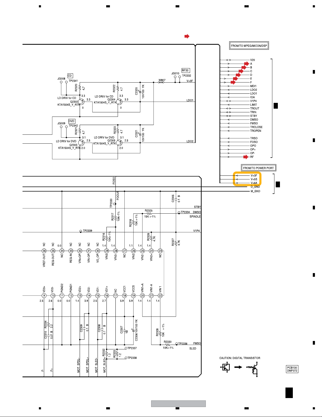
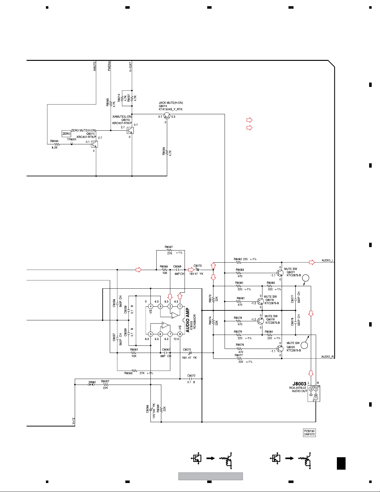
3.7 DVD MT PCB ASSY(4/6)
A
B
C
A 4/6
DVD MT PCB ASSY (A2I802A130)
AUDIO JACK BLOCK
(DA)
(DA)
11
(DA)
(DA)
(DA)
1/6A 6/6A
D
E
F
22
A 4/6
NOTE : THE DC VOLTAGE EACH PART WAS
MEASURED WITH THE DIGITAL TESTER
DURING PLAYBACK.
NOTE : THIS SCHEMATIC DIAGRAM IS THE LATEST AT THE TIME
OF PRINTING AND SUBJECT TO CHANGE WITHOUT NOTICE.
DV-393-S
1234
5678
A
(DA)
: AUDIO SIGNAL ROUTE (Digital)
: AUDIO SIGNAL ROUTE (L ch)
B
10
C
9
D
E
CAUTION : DIGITAL TRANSISTOR CAUTION : DIGITAL TRANSISTOR
DV-393-S
56
F
A 4/6
23
7
8
1234
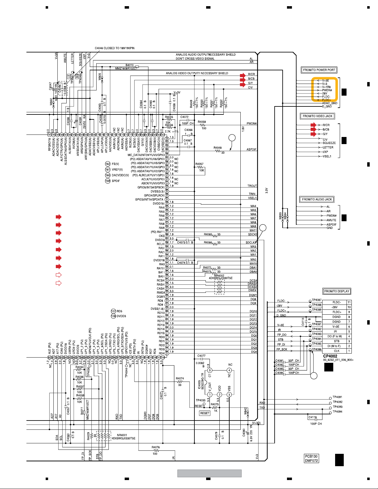
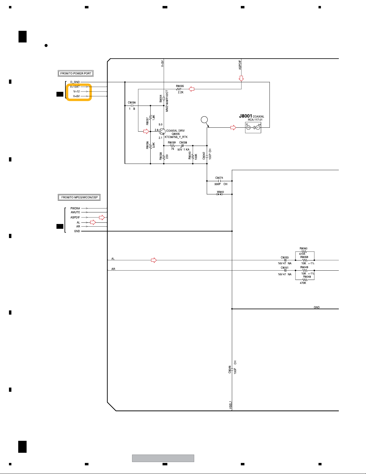
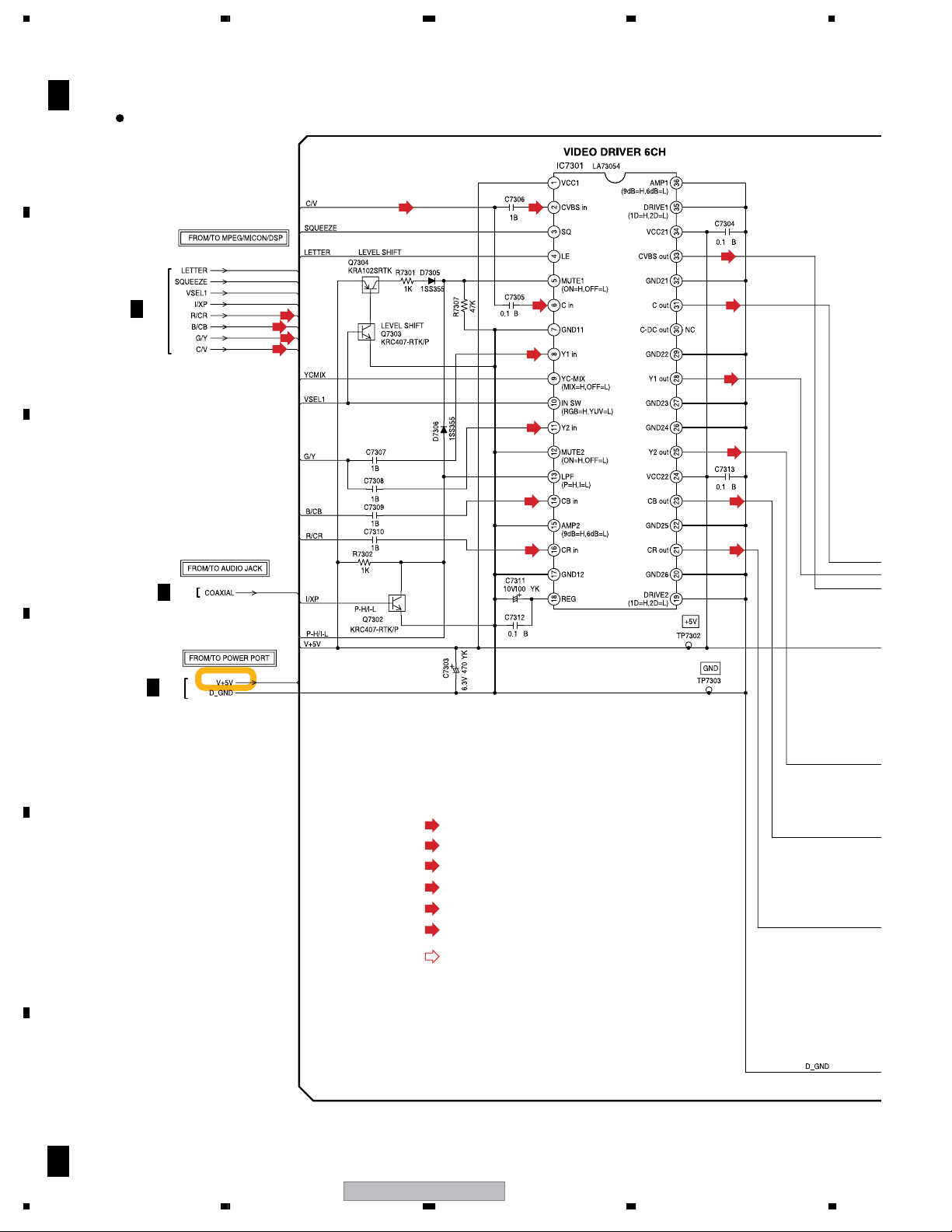
3.8 DVD MT PCB ASSY(5/6)
A
B
C
A 5/6
DVD MT PCB ASSY (A2I802A130)
VIDEO JACK BLOCK
(SC)
1/6A
(R/CR)
(B/CB)
(G/Y)
(SC)
(SC) (SC)
(SY)
(GY)
(B/CB)
(SY)
(GY)
(B/CB)
(R/CR)
(R/CR)
6/6A
6/6
A
D
: VIDEO SIGNAL ROUTE
(SY)
: S VIDEO SIGNAL ROUTE (Y ch)
(SC)
: S VIDEO SIGNAL ROUTE (C ch)
(R/CR)
: VIDEO SIGNAL ROUTE (R/CR ch)
(G/Y)
E
: VIDEO SIGNAL ROUTE (G/Y ch)
(B/CB)
: VIDEO SIGNAL ROUTE (B/CB ch)
: AUDIO SIGNAL ROUTE (L ch)
F
24
A 5/6
NOTE : THE DC VOLTAGE EACH PART WAS
MEASURED WITH THE DIGITAL TESTER
DURING PLAYBACK.
NOTE : THIS SCHEMATIC DIAGRAM IS THE LATEST AT THE TIME
OF PRINTING AND SUBJECT TO CHANGE WITHOUT NOTICE.
DV-393-S
1234
5678
A
(G)
(B)
(R)
CP503
(G)
F 1/2
B
(B)
(R)
C
(SC)
(SY)
D
(G)
(GY)
(R/CR)
(B)
(B/CB)
(R)
(R/CR)
14
15
12
CAUTION: DIGITAL TRANSISTOR
DV-393-S
56
13
CAUTION: DIGITAL TRANSISTOR
7
E
F
A 5/6
25
8
1234
3.9 DVD MT PCB ASSY(6/6)
A
B
C
A 6/6
DVD MT PCB ASSY (A2I802A130)
POWER PORT BLOCK
REG+1.8V IC
IC4006
LM1117S-ADJ
ADJVIN VOUT
123
1.8 0.63.3
W820
R4012
R4011
68 +-1%
FROM/TO POWER
CP4003
D
A2001WV2-14P
CP502
F 1/2
E
(CP502)
1
GND
2
P.CON+12V
3
AT+12V for MUTE
4
GND
5
P.CON+5V
6
P.CON+6V
7
GND(M)
8
AT+3.3V
9
AT+3.3V
10
STBY L
11
GND(D)
12
FL DC-
13
FL DC+
14
-28V
116V B
C4087
C4093
1B
+3.3V
C4112
TP4002
C4086
0.001 B
1B
C4094
C4116
0.1 B
C4095
0.001 B
476.3V KA
15
1B
C4096
39 +-1%
R4013
F
26
ATTENTION
A 6/6
:LES PIECES REPAREES PAR UN ETANT
DANGEREUSES AN POINT DE VUE SECURITE
N’UTILISER QUE CELLS DECRITES
DANS LA NOMENCLATURE DES PIECES.
CAUTION
:SINCE THESE PARTS MARKED BY ARE
CRITICAL FOR SAFETY,USE ONES
DESCRIBED IN PARTS LIST ONLY.
DV-393-S
1234
 Loading...