

Pioneer DJM-909 Service manual

PIONEER CORPORATION 4-1, Meguro 1-chome, Meguro-ku, Tokyo 153-8654, Japan
PIONEER ELECTRONICS (USA) INC. P.O. Box 1760, Long Beach, CA 90801-1760, U.S.A.
PIONEER EUROPE NV Haven 1087, Keetberglaan 1, 9120 Melsele, Belgium
PIONEER ELECTRONICS ASIACENTRE PTE. LTD. 253 Alexandra Road, #04-01, Singapore 159936
PIONEER CORPORATION 2003
PHONO 1
/LINE 1
CD 1
BANK 1 BANK 1
MIC LEVEL
TRIM
BANK 2
0
–
HI
BANK 3
+
–
9
HI
+
FX ADJ. FX ADJ.
12-12
LOW
+
6-26
FADER
CURVE
MID
+
12-12
BANK
EDIT
MIC SEND
+
TIME/SELECT
6-26
LOW
SESSION IN
MIX/DEPTH
+
6
-26
0
–
EQ
CH-1 SEND CH-2 SEND
OFF OFF
MAXMIN
ON
TRANSFORM
FADER START
REVERSE
CH-1 CH-2
10
9
8
7
6
5
4
CH-1 FADER START
3
2
1
0
C.F.1 FADER START
FOOT SW POWER
PROFESSIONAL 2CHANNEL MIXER
DJM-909
EFFECT EFFECT
LOCK ON
OFF
ON
TAP TAP
MASTER LEVEL
LR
14
9
5
3
1
0
–
1
–
3
–
6
–
9
–
15
–
22
dB dB
CH-1 CH-2
REVERSE
PHONO 2
/LINE 2
CD 2
CH-1MIC
MASTER LEVEL
TRIM
BANK 2
0
–
BOOTH/SESSION OUT
BANK 3
+
–
9
HI
0
–
PHONES
+
6-26
FADER
CURVE
MID
0
–
BANK
EDIT
SELECT
MASTER
+
TIME/SELECT
6-26
EFFECT
LOW
CUE
CH-1 CH-2
MIX/DEPTH
+
6-26
EQ
MAXMIN
ON
TRANSFORM
FADER START
REVERSE
14
9
5
10
9
3
8
1
7
0
6
–
1
5
–
3
4
CH-2 FADER START
–
6
3
–
9
2
–
15
1
0
–
22
C.F.2 FADER START
21
FEELING
ADJ.
PHONES
DJM-909
DJ MIXER
DJM-909
THIS MANUAL IS APPLICABLE TO THE FOLLOWING MODEL(S) AND TYPE(S).
Model Type Power Requirement Remarks
DJM-909 KUCXJ AC120V
DJM-909 WYXJ AC220 - 240V
DJM-909 TLTXJ AC110 - 240V
ORDER NO.
RRV2871
For details, refer to "Important symbols for good services" .
T-ZZY DEC. 2003 printed in Japan
1234
SAFETY INFORMATION
A
This service manual is intended for qualified service technicians ; it is not meant for the casual do-ityourselfer. Qualified technicians have the necessary test equipment and tools, and have been trained
to properly and safely repair complex products such as those covered by this manual.
Improperly performed repairs can adversely affect the safety and reliability of the product and may
void the warranty . If you are not qualified to perform the repair of this product properly and safely, you
should not risk trying to do so and refer the repair to a qualified service technician.
WARNING
This product contains lead in solder and certain electrical parts contain chemicals which are known to the state of California to cause
B
cancer, birth defects or other reproductive harm.
Health & Safety Code Section 25249.6 – Proposition 65
C
(FOR USA MODEL ONLY)
1. SAFETY PRECAUTIONS
The following check should be performed for the
continued protection of the customer and service
technician.
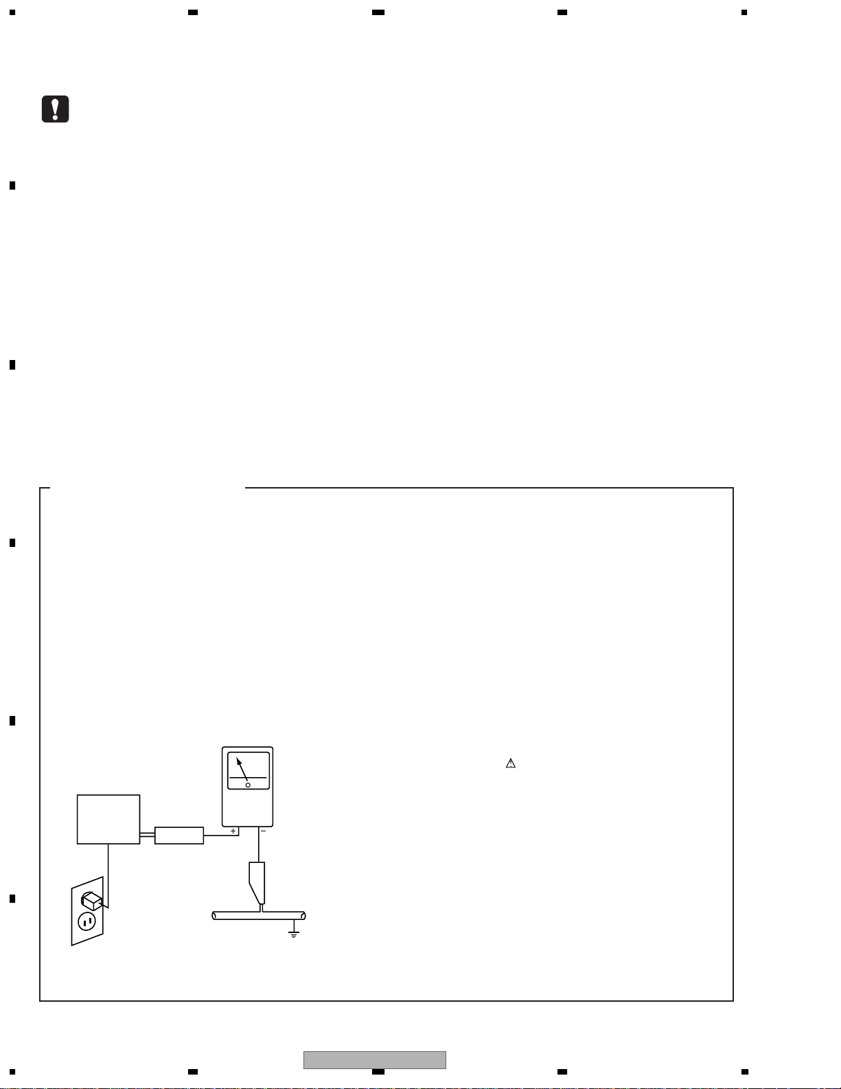
LEAKAGE CURRENT CHECK
Measure leakage current to a known earth ground (water
D
E
pipe, conduit, etc.) by connecting a leakage current tester
such as Simpson Model 229-2 or equivalent between the
earth ground and all exposed metal parts of the appliance
(input/output terminals, screwheads, metal overlays, control
shaft, etc.). Plug the AC line cord of the appliance directly
into a 120V AC 60Hz outlet and turn the AC power switch
on. Any current measured must not exceed 0.5mA.
Reading should
not be above
0.5mA
Earth
ground
Device
under
test
Also test with
plug reversed
(Using AC adapter
plug as required)
Test all
exposed metal
surfaces
Leakage
current
tester
ANY MEASUREMENTS NOT WITHIN THE LIMITS
OUTLINED ABOVE ARE INDICATIVE OF A POTENTIAL
SHOCK HAZARD AND MUST BE CORRECTED BEFORE
RETURNING THE APPLIANCE TO THE CUSTOMER.
2. PRODUCT SAFETY NOTICE
Many electrical and mechanical parts in the appliance
have special safety related characteristics. These are
often not evident from visual inspection nor the protection
afforded by them necessarily can be obtained by using
replacement components rated for voltage, wattage, etc.
Replacement parts which have these special safety
characteristics are identified in this Service Manual.
Electrical components having such features are identified
by marking with a
in this Service Manual.
The use of a substitute replacement component which does
not have the same safety characteristics as the PIONEER
recommended replacement one, shown in the parts list in
this Service Manual, may create shock, fire, or other hazards.
Product Safety is continuously under review and new
instructions are issued from time to time. For the latest
information, always consult the current PIONEER Service
Manual. A subscription to, or additional copies of, PIONEER
Service Manual may be obtained at a nominal charge from
PIONEER.
on the schematics and on the parts list
F
2
1234
AC Leakage Test
DJM-909
5 678
[ Important symbols for good services ]
In this manual, the symbols shown-below indicate that adjustments, settings or cleaning should be made securely.
When you find the procedures bearing any of the symbols, be sure to fulfill them:
1. Product safety
You should conform to the regulations governing the product (safety, radio and noise, and other regulations), and
should keep the safety during servicing by following the safety instructions described in this manual.
2. Adjustments
To keep the original performances of the product, optimum adjustments or specification confirmation is indispensable.
In accordance with the procedures or instructions described in this manual, adjustments should be performed.
A
3. Cleaning
For optical pickups, tape-deck heads, lenses and mirrors used in projection monitors, and other parts requiring cleaning,
proper cleaning should be performed to restore their performances.
4. Shipping mode and shipping screws
To protect the product from damages or failures that may be caused during transit, the shipping mode should be set or
the shipping screws should be installed before shipping out in accordance with this manual, if necessary.
5. Lubricants, glues, and replacement parts
Appropriately applying grease or glue can maintain the product performances. But improper lubrication or applying
glue may lead to failures or troubles in the product. By following the instructions in this manual, be sure to apply the
prescribed grease or glue to proper portions by the appropriate amount.For replacement parts or tools, the prescribed
ones should be used.
CONTENTS
SAFETY INFORMATION......................................................................................................................................2
1. SPECIFICATIONS.............................................................................................................................................5
2. EXPLODED VIEWS AND PARTS LIST.............................................................................................................6
2.1 PACKING....................................................................................................................................................6
2.2 EXTERIOR SECTION ................................................................................................................................8
2.3 CONTROL PANEL (LOWER) SECTION ..................................................................................................10
2.4 CONTROL PANEL (UPPER) SECTION ...................................................................................................12
2.5 FRONT PANEL SECTION........................................................................................................................14
3. BLOCK DIAGRAM AND SCHEMATIC DIAGRAM ..........................................................................................16
3.1 BLOCK DIAGRAM....................................................................................................................................16
3.1.1 OVERALL BLOCK DIAGRAM............................................................................................................16
3.1.2 DSP/ LCD BLOCK DIAGRAM............................................................................................................18
3.2 OVERALL CONNECTION DIAGRAM ......................................................................................................20
3.3 MAIN ASSY (1/6)......................................................................................................................................22
3.4 MAIN ASSY (2/6)......................................................................................................................................24
3.5 MAIN ASSY (3/6)......................................................................................................................................26
3.6 MAIN ASSY (4/6)......................................................................................................................................28
3.7 MAIN ASSY (5/6)......................................................................................................................................30
3.8 MAIN ASSY (6/6)......................................................................................................................................32
3.9 DSP ASSY (1/2) .......................................................................................................................................34
3.10 DSP ASSY (2/2) .....................................................................................................................................36
3.11 C1EQ ASSY (1/2)...................................................................................................................................38
3.12 C1EQ ASSY (2/2)...................................................................................................................................40
3.13 C2EQ ASSY ...........................................................................................................................................42
3.14 C1BF ASSY............................................................................................................................................44
3.15 C2BF ASSY............................................................................................................................................46
3.16 MICB ASSY............................................................................................................................................48
3.17 HPBO ASSY...........................................................................................................................................50
B
C
D
E
F
56
DJM-909
7
8
3

1234
3.18 FDVR ASSY........................................................................................................................................... 52
3.19 SDRT ASSY........................................................................................................................................... 54
3.20 XLR ASSY (1/2)..................................................................................................................................... 56
A
3.21 XLR ASSY (2/2)..................................................................................................................................... 58
3.22 LVMR (1/2), C1TR, C2TR, FVA1 and FVA2 ASSYS.............................................................................. 60
3.23 LVMR ASSY (2/2) ..................................................................................................................................62
3.24 CFVR, RVSW and FSSW ASSYS......................................................................................................... 64
3.25 LCD ASSY .............................................................................................................................................66
3.26 SW POWER SUPPLAY..........................................................................................................................68
3.27 VOLTA GES.............................................................................................................................................69
3.28 WAVEFORMS........................................................................................................................................75
4. PCB CONNECTION DIAGRAM ..................................................................................................................... 80
4.1 MAIN ASSY ............................................................................................................................................. 80
4.2 DSP ASSY............................................................................................................................................... 84
4.3 C1EQ ASSY............................................................................................................................................. 86
B
4.4 C2EQ ASSY............................................................................................................................................. 87
4.5 C1BF ASSY .............................................................................................................................................88
4.6 C2BF ASSY .............................................................................................................................................89
4.7 MICB ASSY ............................................................................................................................................. 90
4.8 HPBO ASSY ............................................................................................................................................91
4.9 LVMR, C1TR, C2TR, FVA1, FVA2 and FDVR ASSYS............................................................................. 92
4.10 LVMR, C1TR, C2TR, FVA1, FVA2 and FDVR ASSYS........................................................................... 94
4.11 SDRT ASSYS ........................................................................................................................................96
4.12 XLR ASSY ............................................................................................................................................. 97
4.13 CFVR, RVSW and FSSW ASSYS......................................................................................................... 98
4.14 LCD ASSY ...........................................................................................................................................100
4.15 SW POWER SUPPLY.......................................................................................................................... 102
C
5. PCB PARTS LIST .........................................................................................................................................104
6. ADJUSTMENT ............................................................................................................................................. 112
6.1 ADJUSTMENT REQUIRED WHEN THE SET IS REPAIRED OR REPLACED..................................... 112
6.2 CH1 OFFSET ADJUSTMENT................................................................................................................114
6.3 CH1 GAIN ADJUSTMENT.....................................................................................................................115
6.4 CH2 OFFSET ADJUSTMENT................................................................................................................116
6.5 CH2 GAIN ADJUSTMENT.....................................................................................................................117
6.6 CH1 EQ Low ADJUSTMENT.................................................................................................................118
6.7 CH1 EQ Mid ADJUSTMENT.................................................................................................................. 119
6.8 CH1 EQ Hi ADJUSTMENT.................................................................................................................... 120
6.9 CH2 EQ Low ADJUSTMENT.................................................................................................................121
6.10 CH2 EQ Mid ADJUSTMENT................................................................................................................ 122
D
6.11 CH2 EQ Hi ADJUSTMENT.................................................................................................................. 123
7. GENERAL INFORMATION...........................................................................................................................124
7.1 DIAGNOSIS........................................................................................................................................... 124
7.1.1 SERVICE MODE............................................................................................................................. 124
7.1.2 Rewriting of the Software.................................................................................................................128
7.1.3 POWER ON SEQUENCE................................................................................................................135
7.1.4 Table of the roles of the microcomputers......................................................................................... 136
7.1.5 DISASSEMBLY................................................................................................................................138
7.1.6 CONFIGURATION OF THE PC BOARD......................................................................................... 144
7.2 PARTS....................................................................................................................................................145
7.2.1 IC INFORMATION........................................................................................................................... 145
8. PANEL FACILITIES AND SPECIFICATIONS ............................................................................................... 150
E
F
4
1234
DJM-909

Audio Section
Input terminal (input level/impedance)
CD 1, 2 ................................................. –14 dBV (200 mV) / 22 kΩ
LINE 1, 2 .............................................. –14 dBV (200 mV) / 47 kΩ
PHONO 1, 2 ............................................. –54 dBV (2 mV) / 47 kΩ
MIC .................................................. ......... –54 dBV (2 mV) / 3 kΩ
SESSION IN ........................................ –14 dBV (200 mV) / 22 kΩ
RETURN ............................................. –14 dBV (200 mV) / 22 kΩ
Output terminal (output level/impedance)
MASTER OUT 1 (XLR) .................................... 0 dBV (1 V) / 600Ω
MASTER OUT 2 (RCA) ................................... 0 dBV (1 V) / 1 kΩ
BOOTH / SESSION OUT ................................ 0 dBV (1 V) / 1 kΩ
SEND .................................................... –14 dBV (200 mV) / 1 kΩ
PHONES ............................................... 6 dBV (2 V) / 22 Ω or less
(Rated load impedance 32 Ω)
Frequency characteristics
CD, LINE, MIC ..................................................... 20 Hz to 20 kHz
PHONO (RIAA) .................................................... 20 Hz to 20 kHz
SN ratio
CD, LINE ........................................ 93 dB or more (EFFECT OFF)
PHONO................................................................... 78 dB or more
MIC ......................................................................... 64 dB or more
Total harmonic distortion rate
CD, LINE ................................................................. 0.02% or less
Cross talk (1 kHz) .................................................... 77 dB or more
Channel equalizer (CD, LINE/PHONO)
HI ........................................................................ +6 dB to –26 dB
MID...................................................................... +6 dB to –26 dB
LOW ................................................................... +6 dB to –26 dB
Microphone equalizer (MIC)
HI ....................................................................... +12 dB to –12 dB
LOW .................................................................. +12 dB to –12 dB
[KUCXJ type]
Electrical Section, etc.
Power supply voltage .......................................... AC 120 V, 60 Hz
Power consumption ............................................................... 31 W
Operating temperature ................ +5 °C to +35 °C (41 °F to 95 °F)
Operating humidity ....................................................... 5% to 85%
External dimensions ............. 251 (W) x 381.6 (D) x 107.9 (H) mm
9-7/8 (W) x 15 (D) x 4-1/4 (H) in
Weight .................................................................................. 6.5 kg
14 lbs 5 oz
Accessories
÷ Hexagonal Allen driver ............................................................. 1
÷ These operating instructions..................................................... 1
÷ Warranty ................................................................................... 1
[WYXJ type]
Electrical Section, etc.
Power supply voltage .............................. AC 220-240 V, 50/60 Hz
Power consumption ............................................................... 30 W
Operating temperature ............................................ +5°C to +35°C
Operating humidity ....................................................... 5% to 85%
External dimensions ............. 251 (W) x 381.6 (D) x 107.9 (H) mm
Weight .................................................................................. 6.5 kg
Accessories
÷ Hexagonal Allen driver ............................................................. 1
÷ These operating instructions..................................................... 1
[TLTXJ type]
Electrical Section, etc.
Power supply voltage .............................. AC 110-240 V, 50/60 Hz
Power consumption ............................................................... 30 W
Operating temperature ........................................... +5°C to +35°C
Operating humidity ....................................................... 5% to 85%
External dimensions ............. 251 (W) x 381.6 (D) x 107.9 (H) mm
Weight .................................................................................. 6.5 kg
Accessories
÷ Hexagonal Allen driver ............................................................. 1
÷ These operating instructions..................................................... 1
For improvement purposes, specifications and design may be subject to
modification without notice.
¶ Operating instructions................... x1
¶ Warranty........................................ x1
¶ Hexagonal Allen driver..........x1
(DEX1018)
Accessories
5 678
1. SPECIFICATIONS
A
B
C
D
DJM-909
56
E
F
7
8
5
1234
2. EXPLODED VIEWS AND PARTS LIST
NOTES:
A
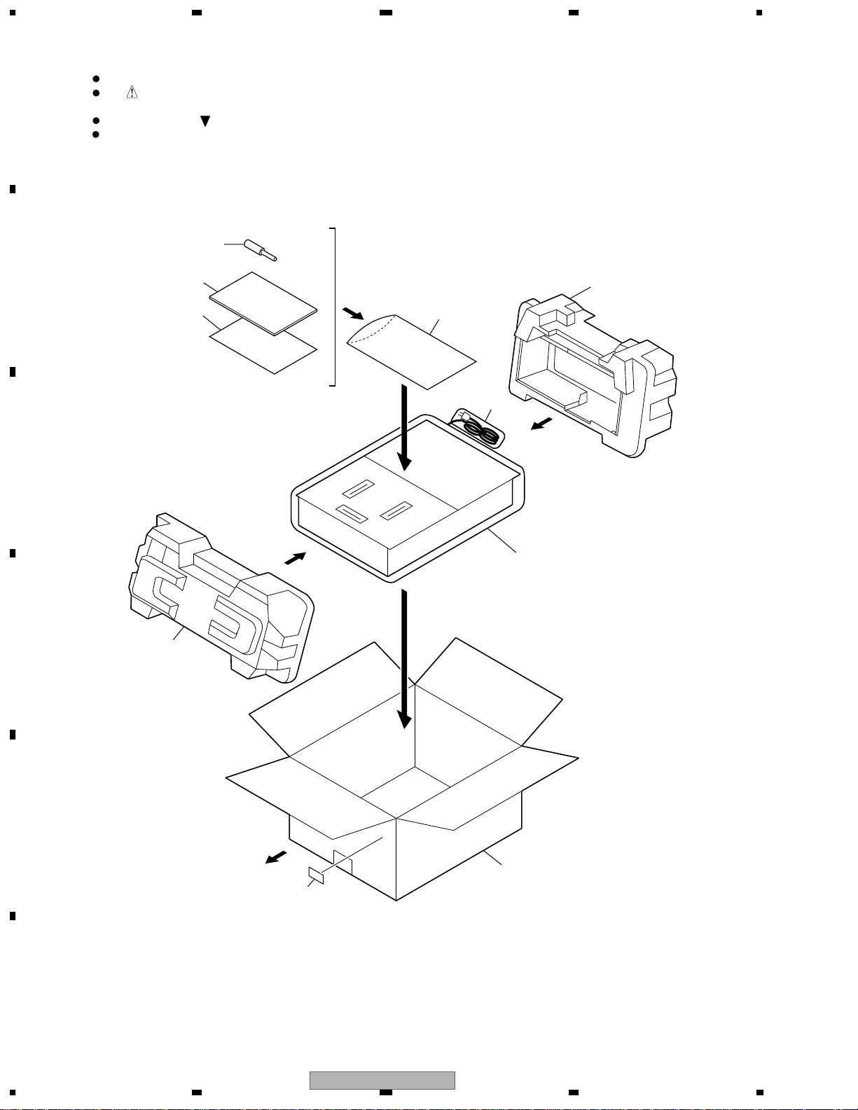
2.1 PACKING
B
C
Parts marked by "NSP" are generally unavailable because they are not in our Master Spare Parts List.
The mark found on some component parts indicates the importance of the safety factor of the part.
Therefore, when replacing, be sure to use parts of identical designation.
Screws adjacent to mark on product are used for disassembly.
For the applying amount of lubricants or glue, follow the instructions in this manual.
(In the case of no amount instructions, apply as you think it appropriate.)
1
3
2
4
8
6
7
D
E
5
FRONT
10
9
F
6
1234
DJM-909
5 678
PACKING parts List
Mark
Mark
No. Description Part No.
1Hexagon Screwdriver DEX1018
NSP 2 Warranty Card See Contrast table(2)
3 Operating Instructions See Contrast table(2)
4Polyethylene Bag Z21-038
(0.03 x 230 x 340)
5Pad (A) DHA1586
No. Description Part No.
6Pad (B) DHA1587
7 Sheet RHX1006
8Polyethylene Bag VHL1051
9Packing Case See Contrast table(2)
NSP 10 Label VRW1629
(2) CONTRAST TABLE
DJM-909/ KUCXJ, DJM-909/ WYXJ and DJM-909/ TLTXJ are constructed the same except for the following :
Mark No. Symbol and Description
NSP 2 Warranty Card ARY7043 Not used Not used
3 Operating Instructions (English) DRB1349 Not used Not used
3 Operating Instructions
(English/ French/ German/ Italian/ Duch/ Spanish)
3 Operating Instructions (English/ Spanish/ Chinese) Not used Not used DRB1351
9Packing Case DHG2441 DHG2440 DHG2442
DJM-909
KUCXJ
Not used DRB1350 Not used
DJM-909
WYXJ
DJM-909
TLTXJ
A
B
C
D
E
56
DJM-909
F
7
8
7
1234
2.2 EXTERIOR SECTION
A
NON-CONTACT
B
C
D
E
SIDE
CONTACT SIDE
49
21
49
23
49
47
Refer to "2.3 CONTROL PANEL (LOWER) SECTION".
48
48
A
11
M
14
49
49
G
9
20
J
10
K
E
2
O
13
12
25
49
18
22
F
26
U
17
49
19
49
K
10
J
24
30
E
B
G
H
27
49
7
49
6
28
E
30
L
I
29
F
C
L
M
49
4
J
15
K
16
49
31
Refer to "2.4 CONTROL PANEL (UPPER) SECTION".
48
48
B
I
O
N
5
3
48
D
F
D
N
H
40
C
B
P
39
49
29
41
21
42
A
36
1
38
49
35
A
49
49
49
49
50
49
49
P
46
33
32
48
43
21
49
52
34
50
49
28
4544
49
50
43
49
37
8
49
49
Refer to "2.5 FRONT PANEL SECTION".
F
8
1234
49
DJM-909
49
49
51
49
51

>
>
>
5 678
EXTERIOR SECTION Parts List
Mark
No. Description Part No.
1 MAIN Assy DWX2337
2 C1BF Assy DWS1328
3 C2BF Assy DWS1329
4 SDRT Assy DWX2321
5 XLR Assy DWX2322
6 DSP Assy DWX2316
7 SW POWER SUPPLY DWR1377
8AC Power Cord See Contrast table(2)
9 Strain Relief See Contrast table(2)
10 Flexible Cable (23P) DDD1239
11 Flexible Cable (15P) DDD1243
12 Flexible Cable (17P) DDD1234
13 Connector Assy (9P) DKP3662
14 Flexible Cable (27P) DDD1242
15 Locking Card Spacer PNW2917
NSP 16 PC Support VEC1584
17 Spacer B DEC2622
18 Shield Sheet G DEC2610
19 Spacer A DEC2617
NSP 20 Shield Case DNH2572
NSP 21 Cord Stopper ZCB-069Z
22 Shield Sheet B DEC2570
23 Shield Sheet C DEC2584
24 Flexible Cable (19P) DDD1238
25 Flexible Cable (35P) DDD1241
26 Connector Assy PF08EE-D15
27 Connector Assy DKP3659
Mark
No. Description Part No.
28 Blind Cap DNK4218
29 Foot REC-434
30 Flexible Cable (17P) DDD1246
31 Cord Stopper Stay DNH2576
NSP 32 Bottom Plate DNH2570
33 Rivet RBM-003
NSP 34 Chassis (9) Assy DXB1815
NSP 35 Partition Plate DNH2573
NSP 36 Chassis (9) DNA1296
NSP 37 Rear Panel See Contrast table(2)
38 Shield Sheet A DEC2569
39 Connector Assy (6P) DKP3661
40 Mini Clamp DEC2588
41 Flexible Cable (11P) DDD1245
42 Card Spacer DNK2769
43 Terminal Screw AKE-031
44 Washer DBE1010
45 Nut NKX2FUC
46 Cord Cover DNK4197
47 Power Knob DAC2133
48 Screw CMZ30P100FZK
49 Screw BBZ30P060FZK
50 Screw BPZ30P080FMC
51 Screw BBZ40P120FMC
52 Connector Assy (8P) DKP3660
A
B
C
(2) CONTRAST TABLE
DJM-909/ KUCXJ, DJM-909/ WYXJ and DJM-909/ TLTXJ are constructed the same except for the following :
Mark No. Symbol and Description
8AC Power Cord VDG1075 VDG1077 VDG1077
>
>
9 Strain Relief CM-22C CM-22B CM-22B
NSP 37 Rear Panel DNC1656 DNC1655 DNC1657
DJM-909
KUCXJ
DJM-909
WYXJ
DJM-909
TLTXJ
D
E
F
56
DJM-909
7
8
9
1234
2.3 CONTROL PANEL (LOWER) SECTION
A
NON-CONTACT
SIDE
CONTACT SIDE
B
8
7
7
49
L
41
33
10
11
12
4
N
KUCXJ
ONLY
40
48
42
13
2
P
B
6
34
42
9
11
42
48
13
42
C
14
50
42
1
O
16
16
17
18
19
43
20
21
43
D
E
22
23
44
25
47
45
26
27
15
24
24
44
29
29
16
17
28
30
16
I
46
47
46
32
5
To. DSP ASSY
(EXTERIOR SECTION: No.24)
33
45
31
37
36
46
B
(EXTERIOR SECTION: No.10)
41
12
A
3
M
34
42
33
B
To. DSP ASSY
41
B
41
34
33
A
35
39
38
F
42
10
1234
DJM-909
38

5 678
CONTROL PANEL (LOWER) SECTION Parts List
Mark
No. Description Part No.
1FVA1 Assy DWX2323
2FVA2 Assy DWX2324
3 C1TR Assy DWS1334
4 C2TR Assy DWS1335
5FDVR Assy DWX2320
Mark
No. Description Part No.
26 Case A DNK4193
27 Worm gear S DNK4195
28 Rack gear S DNK4196
29 MG Shaft DLA1947
30 WG Holder DNF1681
A
6LVMR Assy DWS1330
7 Slider Knob (L) DNK4210
8 Control Panel (D9) DNB1121
9Fader Packing (A) DEC2571
10 Push SW Guide DNK4208
11 SW Packing (A) DEC2573
12 Transform Panel DNF1682
13 CH Fader Bracket DNF1683
14 CR Fader Bracket DNF1684
15 Cross Fader Assy-S DXX2535
16 Washer WT28D060D025
17 O Ring (2.8) DEB1618
18 Slider Base DNK4192
19 Lever Plate DNH2564
20 Fader Magnet DMG1010
21 Yoke DNH2569
22 Encoder Plate S DEC2568
23 Stopper S DNH2578
24 Guide Shaft DLA1966
25 MG Plate Assy DXA1968
31 WG Spring DBK1245
32 Case B DNK4194
33 LED Lens (C) DNK4217
34 Push SW Knob (B) DNK4207
35 LED Lens (B) DNK4216
36 Level Meter Holder DNK4214
37 Flexible Cable (9P) DDD1240
38 Rivet RBM-003
39 Shield Sheet (F) DEC2591
40 65 Label (S) See Contrast table(2)
41 Screw AMZ26P040FMC
42 Screw BBZ30P060FZK
43 Screw BPZ20P060FMC
44 Screw CPZ26P100FZK
45 Screw AMZ20P040FMC
46 Screw BPZ20P050FMC
47 Screw PBA1062
48 Thin Head Screw DBA1198
NSP 49 Panel Stay (D) Assy DXB1787
50 Screw BPZ30P080FMC
B
C
(2) CONTRAST TABLE
DJM-909/ KUCXJ, DJM-909/ WYXJ and DJM-909/ TLTXJ are constructed the same except for the following :
Mark No. Symbol and Description
40 65 Label (S) DRW2164 Not used Not used
DJM-909
KUCXJ
DJM-909
WYXJ
DJM-909
TLTXJ
D
E
F
56
DJM-909
7
8
11

1234
2.4 CONTROL PANEL (UPPER) SECTION
A
B
C
D
NON-CONTACT
SIDE
CONTACT SIDE
14
15
54
56
17
Types of the rotary Knobs (by color)
No.7
6
7
7
8
9
16
52
52
53
A
12
20
17
56
10
20
56
54
15
56
13
54
Gray
Gray
40
12
53
41
(No indicating line)
No.9 No.10
12
20
Red
7
Wide
22
56
9
11
10
18
21
20
55
Wide
No.8No.6
B
RedGray
54
C
39
54
12
42
54
30
31
32
33
34
35
36
37
54
38
43
44
45
23
24
25
26
E
25
To. CIBF ASSY
(EXTERIOR SECTION: No.12)
26
E
3
25
C
1
57
26
60
28
27
D
2
F
To. C2BF ASSY
(EXTERIOR SECTION: No.41)
48
A
55
G
F
12
1234
4
H
DJM-909
55
50
46
47
B
58
5
T
C
55
55
59
55
49
51
5 678
CONTROL PANEL (UPPER) SECTION Parts List
Mark
No. Description Part No.
1 C1EQ Assy DWS1326
2 C2EQ Assy DWS1327
3 MICB Assy DWX2318
4 HPBO Assy DWX2319
5 LCD Assy DWX2317
Mark
No. Description Part No.
31 Touch Panel DSX1062
32 Bracket DNH2574
33 Gasket DEC2632
34 LCD Module DAV1002
35 Diffusion Sheet DEC2619
A
6 Rotary Knob (Small: Gray) DNK4205
7 Rotary Knob (Small: Gray) DNK4203
8 Rotary Knob (Small: Red) DNK4204
9 Rotary Knob (Large: Red) DNK4202
10 Rotary Knob (Large: Glay) DNK4201
11 Slider Knob (S) DNK4211
12 SW Packing (D) DEC2580
13 Escutcheon DNK4222
14 Control Panel (U9) DNB1120
15 Push SW Guide DNK4208
16 SW Packing (C) DEC2621
17 SW Packing (B) DEC2574
18 Fader Packing (B) DEC2572
19 • • • • •
20 Flange Nut DBN1004
21 SW Packing (A) DEC2573
22 65 Label (S) See Contrast table(2)
NSP 23 Panel Stay (U9) DND1250
24 Shield Sheet E DEC2581
25 LED Lens (A) DNK4215
26 Push SW Knob (A) DNK4206
27 Cue Earth Plate DBK1252
28 Flexible Cable (7P) DDD1244
29 • • • • •
30 Earth Plate DNH2577
36 Lighting Conductor DNK4200
37 Reflection Sheet DEC2620
38 LCD Holder DNK4199
39 LCD Holder (M) DNK4225
40 Earth Spring DBK1248
41 Earth Bracket DNH2575
42 Tap Knob DNK4209
43 Preset Knob DNK4306
44 Tact Knob (E) DNK4265
45 Tact Knob DNK4213
46 Shade Sheet DEC2631
47 LED Lens (C) DNK4217
48 Earth Lug Assy DDX1191
49 Shield Sheet D DEC2579
50 Flexible Cable (21P) DDD1237
51 Rivet RBM-003
52 Screw PBA1062
53 Screw AMZ26P040FMC
54 Screw BBZ30P060FZK
55 Screw BPZ30P080FMC
56 Screw CMZ26P050FZK
57 Screw DBA1141
58 Knob Cushion L DEC2656
59 Knob Cushion R DEC2657
60 Cue Fader Bracket DNF1690
B
C
D
(2) CONTRAST TABLE
DJM-909/ KUCXJ, DJM-909/ WYXJ and DJM-909/ TLTXJ are constructed the same except for the following :
Mark No. Symbol and Description
22 65 Label (S) DRW2164 Not used Not used
DJM-909
KUCXJ
DJM-909
56
DJM-909
WYXJ
7
DJM-909
TLTXJ
8
E
F
13
1234
2.5 FRONT PANEL SECTION
A
1
R
4
B
6
To. DSP ASSY
(EXTERIOR SECTION: No.30)
2
B
8
19
9
10
15
12
11
16
20
13
10
11
18
14
C
D
18
15
17
KUCXJ ONLY
18
7
Q
5
NON-CONTACT
SIDE
CONTACT SIDE
6
A
To. MAIN ASSY
(EXTERIOR SECTION: No.39)
3
S
E
F
14
1234
DJM-909

5 678
Parts List
Mark
No. Description Part No.
1RVSW Assy DWS1332
2 CFVR Assy DWS1331
3 FSSW Assy DWS1333
4 Flexible Cable (6P) DDD1235
5 Flexible Cable (3P) DDD1236
Mark
No. Description Part No.
11 Nut NKX2FUC
12 SW Packing (A) DEC2573
13 Flange Nut DBN1004
14 Front Panel (9) DNB1119
15 Rotary Knob (SS) DAA1162
A
6 Rivet RBM-003
7 Slide Packing (B) DEC2590
NSP 8 Front Panel Stay DNH2571
9 Slide SW Packing (A) DEC2589
10 Washer DBE1010
16 Power Knob Guide DNK4198
NSP 17 Caution Label See Contrast table(2)
18 Screw BBZ30P060FZK
19 Screw AMZ26P040FMC
20 Screw PMA30P060FMC
(2) CONTRAST TABLE
DJM-909/ KUCXJ, DJM-909/ WYXJ and DJM-909/ TLTXJ are constructed the same except for the following :
Mark No. Symbol and Description
NSP 17 Caution Label DRW1975 Not used Not used
DJM-909
KUCXJ
DJM-909
WYXJ
DJM-909
TLTXJ
B
C
D
E
F
56
DJM-909
7
8
15
1234
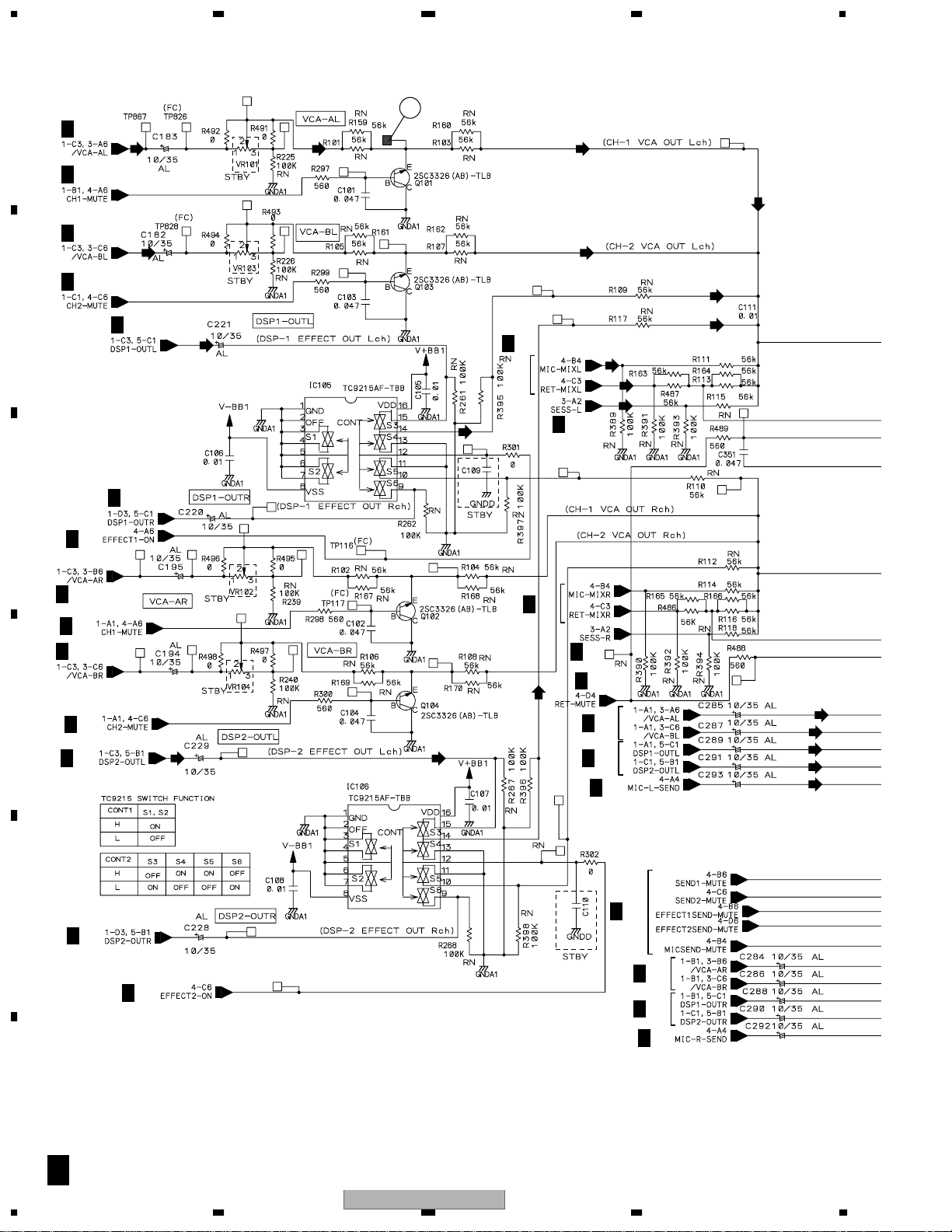
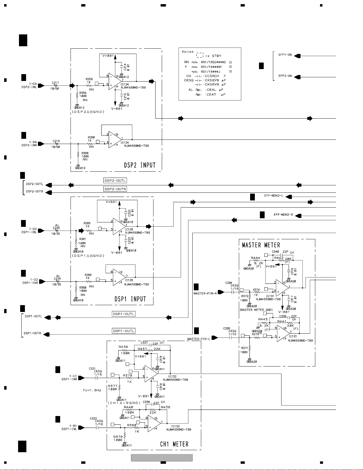
3. BLOCK DIAGRAM AND SCHEMATIC DIAGRAM
3.1 BLOCK DIAGRAM
3.1.1 OVERALL BLOCK DIAGRAM
A
IC1251
JA1251
L
CD
PHONO
/LINE
R
L
R
CH-1
B
C1EQ ASSY
C
2
(1/2)
1
3
IC1604
NJM4580MD
C
NJM5532MD
(1/2)
3 1
(1/2)
3 1
IC1252
NJM5532MD
Buffer
(2/2)
5 7
RIAA
(1/2)
1 3
IC1605
NJM4580MD
LOW
Buffer
1 3
NJM4580MD
3 Band Equalizer
RY1251
2
4
IC1253
NJM5532MD
Phono Amp.
2 5
CH1_OUT_L
CH1_OUT_R
2 5
(1/2)
IC1603
MID
CN1253
(6P)
CN1602
(6P)
JA1202
SESSION
L
R
JA1201
MIC
PHONES
D
G
JA1351
L
CD
PHONO
/LINE
R
L
R
CH-2
E
(1/2)
2 1
NJM2068M
Mic. Amp.
2
3
5 7
IC1201
(1/2)
(2/2)
IC1202
NJM4580MD
Session Amp.
1
MICB ASSY
IC1351
NJM5532MD
Buffer
(1/2)
3 1
(1/2)
3 1
IC1352
NJM5532MD
Buffer
(2/2)
5 7
RIAA
IC1203
NJM2068M
Mix Amp.
(1/2)
2 1
NJM2068M
Gain Amp.
RY1351
2
4
IC1353
NJM5532MD
Phono Amp.
2 5
IC1204
CN1353
(6P)
NJM2068M
4
2
3
(1/2)
1 3
IC1602
NJM4580MD
HI
IC1203
Mic Level
VR1201
(1/2)
3 1
4
2
3
RY1252
VR1602VR1603VR1604
(2/2)
5 7
RY1352
3
7 5
NJM5532MD
CN1202
(6P)
CN1201
3
2
4
(2/2)
IC1601
Buffer
(12P)
2
4
RY1253
CN1254
CN1601
SESSION_IN_L
1
SESSION_IN_R
3
MIC_EQ_IN
6
MIC_EQ_OUT
5
MIC_OUT
12
MIC_TO_CH1
2
RY1353
3
(6P)
(6P)
3
IC1254
NJM5532MD
3 1
IC1255
NJM4580DD
2 1
1 4
CH1_IN_L
CH1_IN_R
1 4
VR1601
TRIM
VR1605
CN1604
(6P)
1
3
6
5
C2BF ASSY
F
IC1355
NJM4580DD
2 1
CN1354
1 4
(6P)
(1/2)
Amp.
(1/2)
VR1606
VR1607
Amp.
(1/2)
E
CN1255
(17P)
CN1603
(17P)
IC1607
NJM4580MD
(2/2)
5 7
LO
2 1
IC1610
HI
NJM4558MD
2Band Equalizer
CN1351
C1BF ASSY
1 3
17 15
(1/2)
CN1252
CN1251
SESSION_OUT_L
SESSION_OUT_R
(18P)
CH1_IN_L
18 18
CH1_IN_R
16 16
CH2_OUT_L
3 3
CH2_OUT_R
1 1
(10P)
CH1_TO2_L
6
CH1_TO2_R
4
MIC_IN_L
10
MIC_IN_R
8 8
(18P)
CH1_OUT_L
3 3
CH1_OUT_R
1 1
SESSION_OUT_R
5 5
SESSION_OUT_L
7 7
NJM4558MD
6 7
NJM4558MD
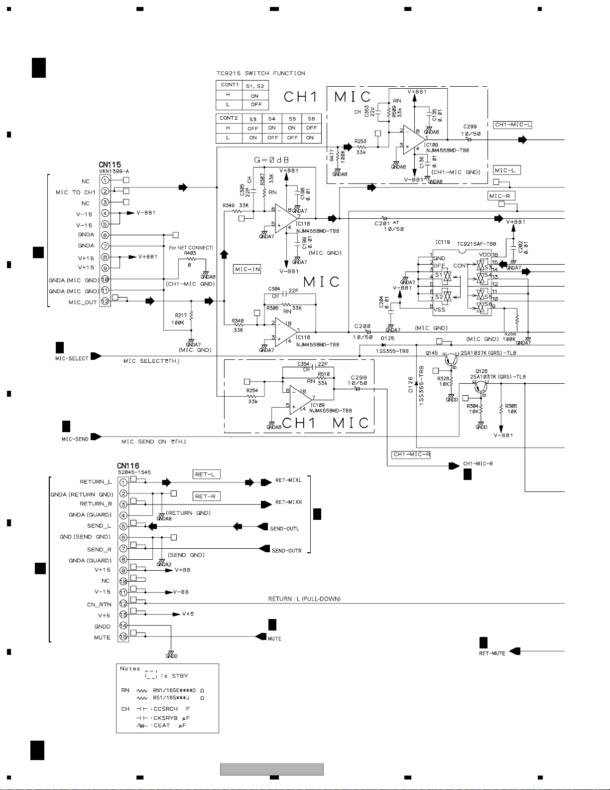
CH1 MIC
12
2 1
2
CN115
(12P)
CN127
(18P)
CN102
(10P)
6
4
10
CN101
(18P)
IC118
MIC
(2/2)
IC109
(1/2)
CH2_IN_L
CH2_OUT_L
CH2_OUT_R
CN1751
2 5
(6P)
6
(2/2)
7
5
IC1754
NJM4580MD
F
(1/2)
1 3
IC1755
NJM4580MD
LOW
(1/2)
1 3
IC1753
NJM4580MD
MID
3 Band Equalizer
16
VR1752VR1753VR1754
(1/2)
1 3
IC1752
NJM4580MD
HI
DJM-909
CN1752
(1/2)
1 3
IC1751
NJM5532MD
Buffer
CH2_IN_R
1 4
(6P)
VR1751
TRIM
C2EQ ASSY
D
VR1755
Monitor
Fader
(1/2)
2 1
IC1748
NJM4558MD
(2/2)
6 7
(1/2)
3 1
IC1750
NJM4558MD
CN1754
(7P)
CUE_L_OUT
2
CUE_R_OUT
6
1
5
3
7
CUE_L1
CUE_R1
CUE_L2
CUE_R2
CN1453
(7P)
6
2
7
3
5
1
1234

IC126
NJM4580MD
DSP1 Input
IC124
NJM4580MD
DSP2 Input
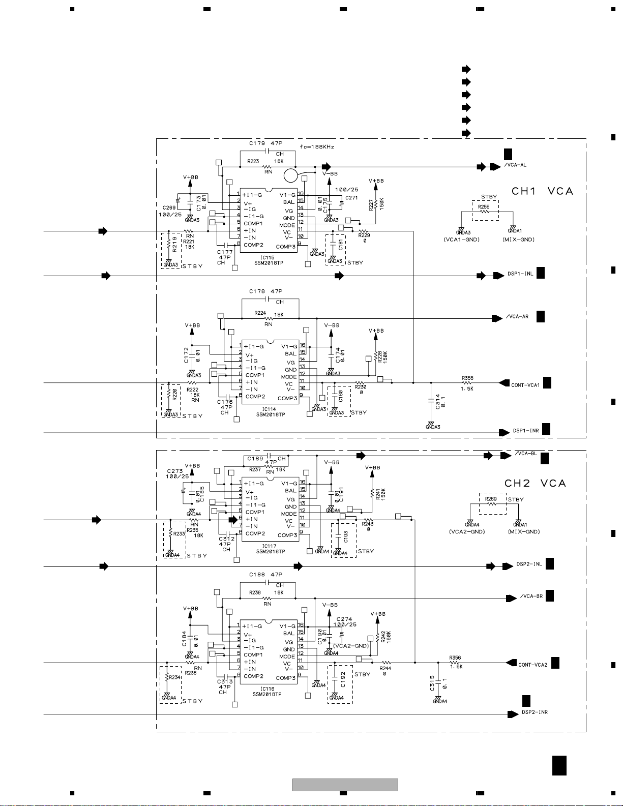
IC115
SSM2018TP
CH1 VCA
6 14
IC117
SSM2018TP
CH2 VCA
6
5 678
A
DSP ASSY
(1/2)
IC1902
(2/2)
IC1901
CH_1_DSP
CH_2_DSP
SESSION
B
XC2S50-5PQ208C
K4S641632F-TC75
HD64F3064BFBL25
CH_1
CH_2
MIC
RETURN
IC714
FPGA
IC713
SDRAM
IC718
CPU
JA1904
JA1903
JA1902
JA1901
L
R
L
R
SEND
RETURN
B
C
(1/2)
3 1
(2/2)
5 7
14
CN117
(35P)
12
10
24
22
20
18
16
14
DSP1ch_IN_L
DSP2ch_IN_L
DSP1ch_OUT_L
8
6
DSP2ch_OUT_L
EFF_MON1_L
4
EFF_MON1_R
2
EFF_MON2_L
EFF_MON2_R
CN705
(35P)
24 2
26
12
14
NJM4580MD
28
30
16
18
32
34
20
22
CH_1_DSP
CH_2_DSP
Effect Mix ON/OFF
Effect Mix ON/OFF
NJM4580MD
(2/2)
6 7
(2/2)
6 7
IC728
1 2
(1/2)
1 2
IC729
NJM4558MD
IC726
NJM4558MD
CH_2
MIC
IC105
TC9215AF
15 14
IC106
TC9215AF
15 14
IC727
IC724
NJM4580MD
(1/2)
IC725
NJM4580MD
(1/2)
1 2
(1/2)
1 2
2 1
NJM4558MD
Send Mix
(1/2)
IC104
IC701
AK5380VT
ADC for CH1
IC700
AK5380VT
2
ADC for CH2
IC703
PCM1742KE
7
DAC for CH1 MIX
IC702
PCM1742KE
7
DAC for CH2 MIX
IC705
PCM1742KE
7
DAC for CH1 HP MONITOT
IC704
PCM1742KE
7
DAC for CH2 HP MONITOT
SEND_LCH_1
5
SEND_R
7
RTN_L
1
RTN_R
3
CN116
(15P)
IC707
DSPA56367PV150
DSP2 for CH1
IC706
DSPA56367PV150
DSP1 for CH2
11
9
15
13
CN1901
(15P)
NJM4558MD
NJM4558MD
Return Amp.
SDRT ASSY
J
3 1
7 6
CN120
(22P)
CN1451
(22P)
2EF_L
2EF_R
2CUE_L
113 17 131 19 5 15
1EF_L
1EF_R
2CUE_R
113 17 131 19 5 15
1CUE_L
VR1451
Master
1CUE_R
Level
XLR ASSY
K
4 28 6
MASTER_IN_L
MASTER_IN_R
MASTER_OUT_L
4 28 6
IC1456
TC9215AF
4 3
(1/2)
3 1
IC1451
NJM5532MD
(2/2)
7 5
IC137
NJM4580MD
CN122
(8P)
MASTER_OUT_R
CN1454
(8P)
7 5
NJM4580MD
NJM5532DD
5 7
IC1453
NJM4580MD
(1/2)
3 1
VR1453
3
4
13
15
11
9
IC102
IC108
Buffer
(2/2)
14
10
(2/2)
Filter
HP Level
NJM5532L
BAL Amp.
2 1
5 7
Booth
Level
IC1454
NJM2068M
(2/2)
5 7
IC1455
TC9215AF
NJM4580MD
VR1452
HP Monitor SW
IC110
(1/2)
(2/2)
IC1452
(1/2)
3 1
RY1451
3 4
MAIN ASSY
A
4
2
CN124
(9P)
JA102
JA103
MASTER2_OUT_L
18
MASTER2_OUT_R
20
BOOTH_OUT_L
14
BOOTH_OUT_R
16
9
11
CN1452
(20P)
FIL_IN_L
FIL_IN_R
L
R
HP_L
HP_R
CN123
(9P)
MASTER1
18
20
14
16
11
CN119
(20P)
1 2
4
2
NJM5532MD
Mix Amp.
IC112
NJM4580DD
MASTER2 Amp.
(1/2)
3 1
CN125
(6P)
9
(1/2)
IC101
CN582
(6P)
L
5
5
R
3
3
S
FSSW ASSY
JA101
L
R
L
R
MASTER2
BOOTH/
SESSION
OUT
JA581
PHONES
D
E
F
HPBO ASSY
H
DJM-909
56
7
8
17
1234
3.1.2 DSP/ LCD BLOCK DIAGRAM
A
276
AIN L
9,10,11,12
SDT0,LRCK,MCLK,SCLK
B
3,5,10,12 1,7,8,14
C
5
51
11 71
SYSCLK
D
V1-V4
DT0-DT15
AD0-AD19
XRESET
63
3
5
185
GCK
VCA1-CONT
95
VCA2-CONT
3
5
LCD ASSY
T
SYSCLK
EXTAL
66
97
E
67
AIN L
2
9,10,11,12
SDT0,LRCK,MCLK,SCLK
F
18
DJM-909
1234
5 678
A
2
TXD,RXD,SCK
2721
VOUT LDATA
B
2721
A0-A6
D8-D20
4
VOUT LDATA
C
66
EXTAL
DSP ASSY
A0-A11
D0-14
FPWM1
12
3
B
1
D
A0-A6
D8-D23
FPWM2
13 12
DATA
DATA
2
2
217
VOUT L
277
VOUT L
DJM-909
56
7
5
E
F
7
8
19

1234
3.2 OVERALL CONNECTION DIAGRAM
A
7P FFC
DDD1244
CH2 EQ Low ADJ.
CH2 EQ Mid ADJ.
CH2 EQ Hi ADJ.
B
11P FFC
DDD1245
C2EQ ASSY (DWS1327)
HPBO ASSY
H
(DWX2319)
CONNECTOR ASSY
DKP3660
D
C
C2BF ASSY (DWS1329)
K
XLR ASSY (DWX2322)
K 1/2 - K 2/2
35P FFC
DDD1241
F
D
17P FFC
DDD1246
A
MAIN ASSY (DWX2337)
E
C 1/2 - C 2/2
C1BF ASSY (DWS1328)
E
A 1/6 - A 6/6
27P FFC
DDD1242
C
C1EQ ASSY (DWS1326)
15P FFC
CH1 EQ Low ADJ.
CH1 EQ Mid ADJ.
CH1 EQ Hi ADJ.
F
20
1234
MICB ASSY
G
(DWX2318)
J
SDRT ASSY
(DWX2321)
DJM-909
DDD1243
CONNECTOR ASSY
DKP3661
FVA1 ASSY
(DWX2323)
O
5 678
A
P
FVA2 ASSY
(DWX2324)
FDVR ASSY
(DWX2320)
I
9P FFC
DDD1240
M
C1TR ASSY
(DWS1334)
CONNECTOR
ASSY
PG03KA-E07
N
C2TR ASSY
(DWS1335)
CONNECTOR
ASSY
PG03KA-E07
L
L 1/2 - L 2/2
LVMR ASSY (DWS1330)
23P FFC
DDD1239
CH1 Offset ADJ.
CH2 Offset ADJ.
CH1 Gain ADJ.
CH2 Gain ADJ.
B
B 1/2 - B 2/2
DSP ASSY (DWX2316)
19P FFC
DDD1238
21P FFC
DDD1237
17P FFC
DDD1234
TOUCH PANEL
(DSX1062)
LCD MODULE
(DAV1002)
LCD ASSY (DWX2317)
T
3P FFC
DDD1236
6P FFC
DDD1235
CFVR ASSY
(DWS1331)
FSSW ASSY
(DWS1333)
B
C
S
D
CONNECTOR
ASSY
PF08EE-D15
CONNECTOR ASSY
DKP3659
÷
When ordering service parts, be sure to refer to "EXPLODED VIEWS and PARTS LIST" or
"PCB PARTS LIST".
÷
The > mark found on some component parts indicates the importance of the safety factor
of the part. Therefore, when replacing, be sure to use parts of identical designation.
÷
: The power supply is shown with the marked box.
DJM-909
56
7
Q
U
SW POWER
SUPPLY
(DWR1377)
POWER CORD
KUCXJ : VDG1075
WYXJ : VDG1077
TLTXJ : VDG1077
8
R
RVSW ASSY
(DWS1332)
21
E
F
1234
3.3 MAIN ASSY (1/6)
A
3/6A
(CH1)
A
4/6
3/6
A
(CH2)
4/6
A
B
5/6
A
A
C
A
4/6
(CH1_D)
5/6
(CH1) (CH1)
EFFECT MIX
ON/OFF
16
(CH1_D)
(CH1)
(CH2)
(CH1_D)
(CH2_D)
4/6
A
(MIC)
(RET)
(SES)
3/6
A
3/6
A
4/6
A
3/6
A
D
E
A
4/6
5/6
A
5/6
A
(CH2_D) (CH2_D)
A
4/6
EFFECT MIX
ON/OFF
4/6
A
(CH2_D)
3/6
A
4/6
A
(CH1)
3/6
A
5/6
A
4/6
A
4/6
A
A
3/6
(CH2)
(CH1_D)
(CH2_D)
(MIC)
5/6A
4/6
A
F
A 1/6
22
1234
DJM-909

5 678
17
1/2K
CN124
A 1/6
(CH1)
(CH2)
(CH1_D)
(CH2_D)
(MIC)
(SEND)
(RET)
(SES)
MAIN ASSY (DWX2337)
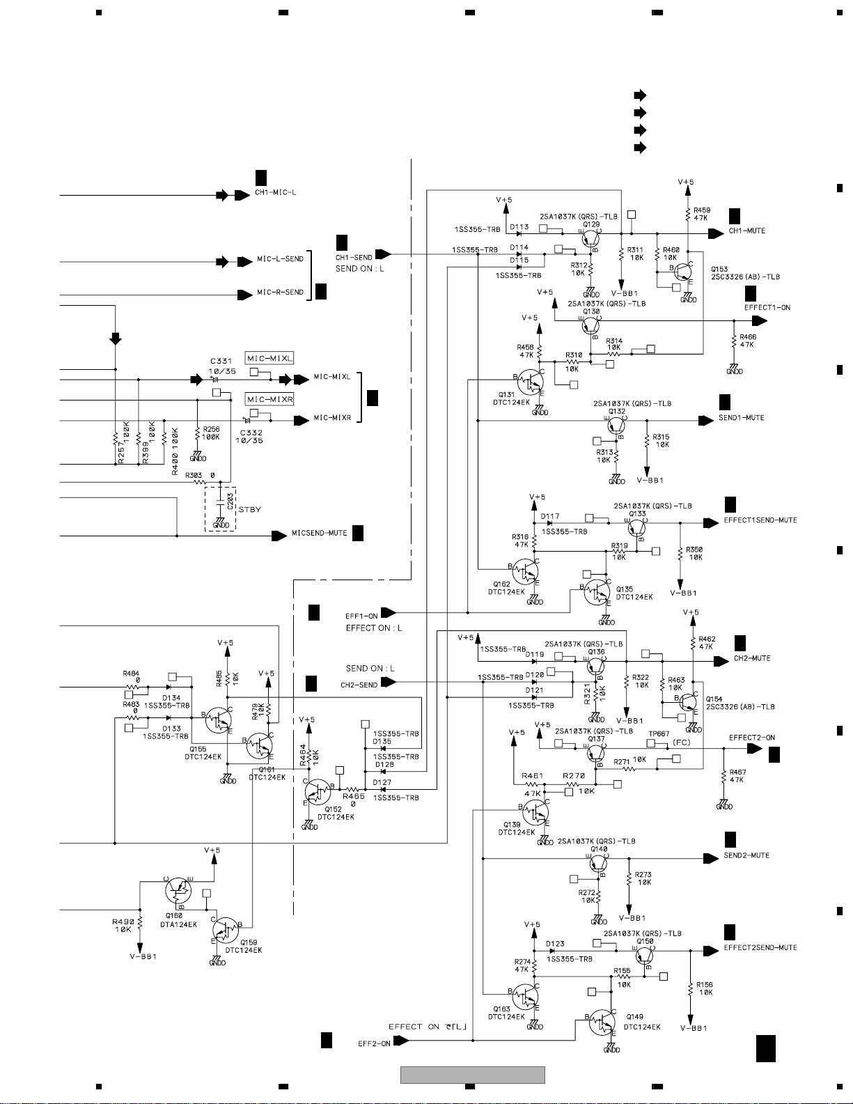
• MIX AMP. BLOCK
: Main Signal Route
: Channel_1 Main Signal Route
: Channel_2 Main Signal Route
: Channel_1 DSP Signal Route
: Channel_2 DSP Signal Route
: Microphone Signal Route
: Send Signal Route
: Return Signal Route
: Session Signal Route
A
B
C
28
2/6, 4/6-6/6
A
• SEND MIX BLOCK
(CH1)
(CH2)
(CH1_D) (CH1_D)
(CH2_D) (CH2_D)
(MIC) (MIC)
(CH1)
(CH2)
(SEND)
29
D
4/6A
E
A
4/6
56
DJM-909
F
A 1/6
7
8
23

1234
3.4 MAIN ASSY (2/6)
A
B
C
A 2/6
MAIN ASSY (DWX2337)
23
(MA_2)
5/6, 6/6A
A
1/6
D
E
F
A 2/6
24
1234
DJM-909

5 678
A
(MA_2)
(BOOTH)
: MASTER_2 Signal Route
: Booth Signal Route
B
(MA_2)
(MA_2) (MA_2)
6/6A
(BOOTH)
UPPER
24
(MA_2)
(BOOTH)
27
C
D
LOWER
DJM-909
56
E
F
A 2/6
7
8
25

1234
3.5 MAIN ASSY (3/6)
A
B
C
A 3/6
E
MAIN ASSY (DWX2337)
CN1251
(SES)
(CH1)
13
(MIC_TH)
4/6A
A
4/6
A
4/6
A
1/6
4/6
A
(CH1)
14
(CH1)
(CH1_D)
(CH1)
CN1252
E
D
E
CN1351
F
(CH1)
(CH2)
(CH1)
(CH2_D)
(CH2)
5/6A
F
A 3/6
26
A
4/6
(CH2) (CH2)
1234
DJM-909
5 678
(CH1)
(CH2)
(CH1_D)
(CH2_D)
(MIC_TH)
(SES)
: Channel_1 Main Signal Route
: Channel_2 Main Signal Route
: Channel_1 DSP Signal Route
: Channel_2 DSP Signal Route
: Microphone Through Signal Route
: Session Signal Route
A
(CH1)
15
(CH1)
(CH1_D)(CH1_D)(CH1_D)
(CH1)
1/6A
B
5/6, 6/6
A
1/6
A
C
5/6
A
5/6, 6/6
A
(CH2)
(CH2_D)
(CH2)
A
(CH2)(CH2)
(CH2_D)(CH2_D)
1/6
A
5/6, 6/6
1/6
A
D
E
5/6A
A
5/6, 6/6
F
56
DJM-909
A 3/6
7
8
27
1234
3.6 MAIN ASSY (4/6)
A
B
C
A 4/6
CN1201
G
3/6A
MAIN ASSY (DWX2337)
(MIC_TH)
(MIC) (MIC)
(MIC)
(MIC_TH)
(MIC)
(MIC)
MIC MIX
ON/OFF
(MIC_TH)
(MIC)
(MIC)
(MIC)
3/6
A
D
A
3/6
CN1901
(RET) (RET)
(SEND) (SEND)
1/6
A
J
E
1/6
A
A
1/6
F
A 4/6
28
1234
DJM-909
5 678
(MIC)
(MIC_TH)
(MIC_TH)
CONTROL
: Microphone Signal Route
: Microphone Through Signal Route
(SEND)
: Send Signal Route
(RET)
: Return Signal Route
3/6A
A
1/6
3/6
A
A
(MIC)
(MIC)
(MIC)
(MIC)
B
1/6
A
A
1/6
A
1/6
5/6
A
A
1/6
1/6
A
C
1/6
A
A
1/6
D
A
3/6
A
5/6
56
DJM-909
1/6
A
E
A
1/6
A
1/6
F
A 4/6
7
8
29
1234
3.7 MAIN ASSY (5/6)
A
B
C
A 5/6
3/6, 6/6A
A
3/6, 6/6
1/6A
MAIN ASSY (DWX2337)
(CH2_D)
(CH2_D)
(CH2_D)
A
4/6
(CH2_D)
(CH2_D)(CH2_D)(CH2_D)
6/6
A
(CH1_D)(CH1_D)
3/6
A
D
A
3/6
(CH1_D)
1/6A
E
A
3/6, 6/6
(CH1_D)
2/6, 6/6
A
(CH1_D)(CH1_D)
2/6, 6/6
A
(CH1_D)
6/6A
F
A 5/6
30
3/6, 6/6
A
1234
DJM-909
 Loading...