

PIONEER CORPORATION 4-1, Meguro 1-chome, Meguro-ku, Tokyo 153-8654, Japan
PIONEER ELECTRONICS (USA) INC. P.O. Box 1760, Long Beach, CA 90801-1760, U.S.A.
PIONEER EUROPE NV Haven 1087, Keetberglaan 1, 9120 Melsele, Belgium
PIONEER ELECTRONICS ASIACENTRE PTE. LTD. 253 Alexandra Road, #04-01, Singapore 159936
PIONEER CORPORATION 2009
CD RECEIVER
ORDER NO.
CRT4478
DEH-2200UB
DEH-2250UB
This service manual should be used together with the following manual(s) listed below.
For the parts numbers, adjustments, etc. which are not shown in this manual,
refer to the following manual(s).
Model No. Order No. Mech. Module Remarks
/XSES
/XSUC
DEH-22UB/XSUC CRT4454
CX-3269 CRT4488 S11iPod/USB CD Mech. Module : Circuit Descriptions, Mech. Descriptions, Disassembly
K-ZZZ. SEPT. 2009 Printed in Japan
1234
1 234
C
D
F
A
B
E
SAFETY INFORMATION
WARNING
This product may contain a chemical known to the State of California to cause cancer, or birth defects or other reproductive
harm.
Health & Safety Code Section 25249.6 - Proposition 65
EXPLODED VIEWS AND PARTS LIST
PACKING(Page 32)
PACKING SECTION PARTS LIST *:Non spare part
Mark No. Description DEH-22UB/XSUC DEH-2200UB/XSUC DEH-2250UB/XSES
11 Unit Box YHG5557 YHG5556 YHG5533
12 Contain Box YHL5557 YHL5556 YHL5533
* 15-1 Warranty Card CRY1276 CRY1276 Not used
15-2 Owner's Manual YRD5305 YRD5301 YRD5302
1 Polyethylene Bag CEG1173 CEG1173 QEG3001
4 Screw BPZ20P060FTC BPZ20P060FTC Not used
7 Screw Assy YEA5072 YEA5072 YEA5082
9 Screw CRZ50P090FTC CRZ50P090FTC Not used
13 Protector YHP5071 YHP5071 YHP5069
14 Protector YHP5072 YHP5072 YHP5070
16 Case Assy Not used Not used YXB5009
Owner's Manual
Part No. Language
YRD5301 English, French, Spanish(Espanol)
YRD5302 English, Spanish(Espanol), Portuguese(B), Traditional Chinese, Arabic
EXTERIOR(1)(Page 34)
EXTERIOR(1) SECTION PARTS LIST
Mark No. Description DEH-22UB/XSUC DEH-2200UB/XSUC DEH-2250UB/XSES
7 Detachable Assy YXA5680 YXA5668 YXA5669
24 Grille Unit YXA5688 YXA5643 YXA5641
25 Knob Unit YXC5124 YXC5123 YXC5123
EXTERIOR(2)(Page 36)
EXTERIOR(2) SECTION PARTS LIST
Mark No. Description DEH-22UB/XSUC DEH-2200UB/XSUC DEH-2250UB/XSES
7 CD Mechanism Module(S11) CXK5870 CXK5860 CXK5860
10 Tuner Amp Unit YWM5449 YWM5429 YWM5430
17 Holder YND5045 YND5045 YND5043
2
DEH-2200UB/XSUC
5 678
56
7
8
C
D
F
A
B
E
ELECTRICAL PARTS LIST(Page 66)
TUNER AMP UNIT
Circuit Symbol and No. Part Name DEH-22UB/XSUC DEH-2200UB/XSUC DEH-2250UB/XSES
D601 Diode Not used Not used RB551V-30
D602 Diode Not used Not used RB751V-40
CN941 Connector Not used Not used CKS4124
R676 Not used RS1/16SS473J Not used
R677 RS1/16SS473J Not used RS1/16SS473J
R680 RS1/16SS273J RS1/16SS273J Not used
R941 Not used Not used RS1/10SR102J
R942 Not used Not used RS1/10SR102J
C941 Not used Not used CKSRYB103K50
C942 Not used Not used CKSRYB103K50
For the information of the parts that are added to this model, please refer to the following manual (CRT4454).
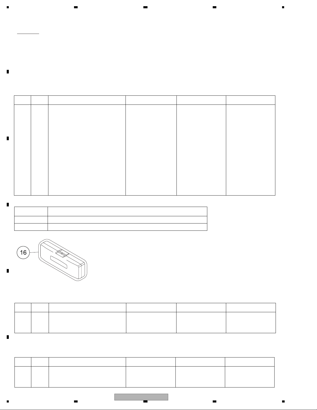
KEYBOARD UNIT
Circuit Symbol and No. Part Name DEH-22UB/XSUC DEH-2200UB/XSUC DEH-2250UB/XSES
Q1851 Transistor Not used IMX9 Not used
D1871 LED Not used CL-195PG-CD Not used
D1872 LED Not used CL-195PG-CD Not used
D1873 LED Not used CL-195PG-CD Not used
D1874 LED Not used CL-195PG-CD Not used
D1875 LED Not used CL-195PG-CD Not used
D1876 LED Not used CL-195PG-CD Not used
D1880 LED Not used CL-195PG-CD Not used
D1881 LED Not used CL-195PG-CD Not used
D1882 LED Not used CL-195PG-CD Not used
D1883 LED Not used CL-195PG-CD Not used
D1884 LED Not used CL-195PG-CD Not used
D1885 LED Not used CL-195PG-CD Not used
D1886 LED Not used CL-195PG-CD Not used
D1887 LED Not used CL-195PG-CD Not used
D1888 LED Not used CL-195PG-CD Not used
D1889 LED Not used CL-195PG-CD Not used
R1859 Not used RS1/4SA561J Not used
R1860 Not used RS1/4SA561J Not used
R1862 Not used RS1/4SA561J Not used
R1863 Not used RS1/4SA561J Not used
R1864 Not used RS1/4SA681J Not used
R1865 Not used RS1/4SA681J Not used
R1866 RS1/10SR0R0J Not used RS1/10SR0R0J
R1867 Not used RS1/10SR103J Not used
R1868 Not used RS1/10SR103J Not used
R1869 Not used RS1/10SR103J Not used
R1870 Not used RS1/10SR103J Not used
DEH-2200UB/XSUC
3
1234
1 234
C
D
F
A
B
E
B
DEH-2200UB/XSUC
DEH-2250UB/XSES
RED
CL-195SR-CD
RED
CL-195SR-CD
NM
GREEN
CL-195PG-CD
DS1XA4WBETW1(Z1)
CLOCK
SCHEMATIC DIAGRAM
KEYBOARD UNIT
4
DEH-2200UB/XSUC
5 678
56
7
8
C
D
F
A
B
E
B
DEH-2200UB
/XSUC
DEH-2250UB
/XSES
CL-195SR-CDCL-195SR-CD
CL-195PG-CD
820(1/4W)
820(1/4W)
1k(1/4W)
1k(1/4W)
560(1/4W)
560(1/4W)
NM
NM
NM
UC
A
CN832
USB
AUX
AUX1:-17.8 dBs
B
KEYBOARD UNIT
DEH-2200UB/XSUC
5
1234
1 234
C
D
F
A
B
E
CD CORE UNIT
Circuit Symbol and No. Part Name DEH-22UB/XSUC
DEH-2200UB/XSUC
DEH-2250UB/XSES
IC205 IC Not used 341S2162
Q201 Transistor Not used 2SA1577
R250 Not used RS1/16SS101J
R252 Not used RS1/16SS101J
R273 Not used RS1/16SS103J
R277 Not used RS1/16SS103J
R280 RS1/16SS103J Not used
R290 RS1/16SS103J Not used
R292 Not used RS1/16SS272J
R293 Not used RS1/16SS472J
R295 Not used RS1/16SS473J
C290 Not used CKSSYB104K10
C294 Not used CKSSYB104K10
For the information of the parts that are added to this model, please refer to the following manual (CRT4454).
6
DEH-2200UB/XSUC
PIONEER CORPORATION 4-1, Meguro 1-chome, Meguro-ku, Tokyo 153-8654, Japan
PIONEER ELECTRONICS (USA) INC. P.O. Box 1760, Long Beach, CA 90801-1760, U.S.A.
PIONEER EUROPE NV Haven 1087, Keetberglaan 1, 9120 Melsele, Belgium
PIONEER ELECTRONICS ASIACENTRE PTE. LTD. 253 Alexandra Road, #04-01, Singapore 159936
PIONEER CORPORATION 2009
CD RECEIVER
ORDER NO.
CRT4454
DEH-22UB/XSUC
DEH-22UB
This service manual should be used together with the following manual(s):
Model No. Order No. Mech. Module Remarks
CX-3269 CRT4488
S11iPod/USB
CD Mech. Module : Circuit Descriptions, Mech. Descriptions, Disassembly
/XSUC
For details, refer to "Important Check Points for Good Servicing".
K-ZZZ. SEPT. 2009 Printed in Japan

1234
1234
C
D
F
A
B
E
SAFETY INFORMATION
CAUTION
Where in a manufacturer’s service documentation, for example in circuit diagrams or lists
of components, a symbol is used to indicate that a specific component shall be replaced only
by the component specified in that documentation for safety reasons, the following symbol shall
be used:
This service manual is intended for qualified service technicians; it is not meant for the casual do-it-yourselfer.
Qualified technicians have the necessary test equipment and tools, and have been trained to properly and safely repair
complex products such as those covered by this manual.
Improperly performed repairs can adversely affect the safety and reliability of the product and may void the warranty.
If you are not qualified to perform the repair of this product properly and safely, you should not risk trying to do so
and refer the repair to a qualified service technician.
CAUTION:
USE OF CONTROLS OR ADJUSTMENTS OR PERFORMANCE OF PROCEDURES OTHER THAN THOSE
SPECIFIED HEREIN MAY RESULT IN HAZARDOUS RADIATION EXPOSURE.
- Safety Precautions for those who Service this Unit.
When checking or adjusting the emitting power of the laser diode exercise caution in order to get safe, reliable
results.
Caution:
1. During repair or tests, minimum distance of 13 cm from the focus lens must be kept.
CAUTION
CLASS 1M INVISIBLE LASER RADIATION WHEN OPEN. DO NOT VIEW DIRECTLY WITH OPTICAL INSTRUMENTS
2. During repair or tests, do not view laser beam for 10 seconds or longer.
WARNING
This product may contain a chemical known to the State of California to cause cancer, or birth defects or
other reproductive harm.
Health & Safety Code Section 25249.6 - Proposition 65
2
DEH-22UB/XSUC
5 678
56
7
8
C
D
F
A
B
E
[Important Check Points for Good Servicing]
In this manual, procedures that must be performed during repairs are marked with the below symbol.
Please be sure to confirm and follow these procedures.
1. Product safety
Please conform to product regulations (such as safety and radiation regulations), and maintain a safe servicing environment by
following the safety instructions described in this manual.
1 Use specified parts for repair.
Use genuine parts. Be sure to use important parts for safety.
2 Do not perform modifications without proper instructions.
Please follow the specified safety methods when modification(addition/change of parts) is required due to interferences such as
radio/TV interference and foreign noise.
3 Make sure the soldering of repaired locations is properly performed.
When you solder while repairing, please be sure that there are no cold solder and other debris.
Soldering should be finished with the proper quantity. (Refer to the example)
4 Make sure the screws are tightly fastened.
Please be sure that all screws are fastened, and that there are no loose screws.
5 Make sure each connectors are correctly inserted.
Please be sure that all connectors are inserted, and that there are no imperfect insertion.
6 Make sure the wiring cables are set to their original state.
Please replace the wiring and cables to the original state after repairs.
In addition, be sure that there are no pinched wires, etc.
7 Make sure screws and soldering scraps do not remain inside the product.
Please check that neither solder debris nor screws remain inside the product.
8 There should be no semi-broken wires, scratches, melting, etc. on the coating of the power cord.
Damaged power cords may lead to fire accidents, so please be sure that there are no damages.
If you find a damaged power cord, please exchange it with a suitable one.
9 There should be no spark traces or similar marks on the power plug.
When spark traces or similar marks are found on the power supply plug, please check the connection and advise on secure
connections and suitable usage. Please exchange the power cord if necessary.
a Safe environment should be secured during servicing.
When you perform repairs, please pay attention to static electricity, furniture, household articles, etc. in order to prevent injuries.
Please pay attention to your surroundings and repair safely.
2. Adjustments
To keep the original performance of the products, optimum adjustments and confirmation of characteristics within specification.
Adjustments should be performed in accordance with the procedures/instructions described in this manual.
4. Cleaning
For parts that require cleaning, such as optical pickups, tape deck heads, lenses and mirrors used in projection monitors, proper
cleaning should be performed to restore their performances.
3. Lubricants, Glues, and Replacement parts
Use grease and adhesives that are equal to the specified substance.
Make sure the proper amount is applied.
5. Shipping mode and Shipping screws
To protect products from damages or failures during transit, the shipping mode should be set or the shipping screws should be
installed before shipment. Please be sure to follow this method especially if it is specified in this manual.
DEH-22UB/XSUC
3

1234
1234
C
D
F
A
B
E
CONTENTS
SAFETY INFORMATION ..................................................................................................................................... 2
1. SERVICE PRECAUTIONS ............................................................................................................................... 5
1.1 SERVICE PRECAUTIONS......................................................................................................................... 5
1.2 NOTES ON SOLDERING .......................................................................................................................... 6
2. SPECIFICATIONS ............................................................................................................................................ 7
2.1 SPECIFICATIONS...................................................................................................................................... 7
2.2 DISC/CONTENT FORMAT ........................................................................................................................ 7
2.3 PANEL FACILITIES .................................................................................................................................... 8
2.4 CONNECTION DIAGRAM ....................................................................................................................... 10
3. BASIC ITEMS FOR SERVICE........................................................................................................................ 11
3.1 CHECK POINTS AFTER SERVICING..................................................................................................... 11
3.2 PCB LOCATIONS .................................................................................................................................... 11
3.3 JIGS LIST ................................................................................................................................................ 12
3.4 CLEANING............................................................................................................................................... 12
4. BLOCK DIAGRAM.......................................................................................................................................... 14
5. DIAGNOSIS.................................................................................................................................................... 17
5.1 OPERATIONAL FLOWCHART ................................................................................................................ 17
5.2 ERROR CODE LIST ................................................................................................................................ 18
5.3 CONNECTOR FUNCTION DESCRIPTION............................................................................................. 20
6. SERVICE MODE ............................................................................................................................................ 21
6.1 DISPLAY TEST MODE ............................................................................................................................ 21
6.2 CD TEST MODE...................................................................................................................................... 22
7. DISASSEMBLY............................................................................................................................................... 23
8. EACH SETTING AND ADJUSTMENT ........................................................................................................... 29
8.1 CD ADJUSTMENT................................................................................................................................... 29
8.2 CHECKING THE GRATING AFTER CHANGING THE PICKUP UNIT.................................................... 30
9. EXPLODED VIEWS AND PARTS LIST.......................................................................................................... 32
9.1 PACKING ................................................................................................................................................. 32
9.2 EXTERIOR(1) .......................................................................................................................................... 34
9.3 EXTERIOR(2) .......................................................................................................................................... 36
9.4 CD MECHANISM MODULE..................................................................................................................... 38
10. SCHEMATIC DIAGRAM ............................................................................................................................... 40
10.1 TUNER AMP UNIT(GUIDE PAGE) ........................................................................................................ 40
10.2 KEYBOARD UNIT.................................................................................................................................. 46
10.3 CD MECHANISM MODULE(GUIDE PAGE) .......................................................................................... 48
10.4 WAVEFORMS........................................................................................................................................ 54
11. PCB CONNECTION DIAGRAM ................................................................................................................... 58
11.1 TUNER AMP UNIT................................................................................................................................. 58
11.2 KEYBOARD UNIT.................................................................................................................................. 62
11.3 CD CORE UNIT(S11USB)..................................................................................................................... 64
12. ELECTRICAL PARTS LIST .......................................................................................................................... 66
4
DEH-22UB/XSUC
5 678
56
7
8
C
D
F
A
B
E
1. You should conform to the regulations governing the product (safety, radio and noise, and other
regulations), and should keep the safety during servicing by following the safety instructions
described in this manual.
2. Before disassembling the unit, be sure to turn off the power. Unplugging and plugging the connectors
during power-on mode may damage the ICs inside the unit.
3. To protect the pickup unit from electrostatic discharge during servicing, take an appropriate treatment
(shorting-solder) by referring to "the DISASSEMBLY".
4. After replacing the pickup unit, be sure to check the grating.
5. Be careful in handling ICs. Some ICs such as MOS type are so fragile that they can be damaged by
electrostatic induction.
6. On CD Core Unit, actual cable colors and silk print are different.
7. CD Mech. Assembly Wrong Installation Check
If iPod corresponding mech. assembly is installed at iPod non corresponding model, or if iPod non corresponding
mech. assembly is installed at iPod corresponding model by mistake, this becomes error indication with CDS,
USB sources as shown below;
Judgment condition of wrong installation is as follows;
* The condition becomes as shown above since a microcomputer of corresponding USB mech. assembly and a
microcomputer of iPod corresponding mech. assembly are the same.
However, this is determined by the presence or absence of authentication IC since problem occurs depending on
different mech. assembly.
Green Red
White Black
Wrong Inst. Error of
CD Mech. Assembly
CHK CD C O R E
USB Corresponding Model
Authentication IC: No OK
Authentication IC: Yes Wrong Installation Indication
Authentication IC: No OK
Authentication IC: Yes Wrong Installation Indication
USB/iPod Corresponding Model
Authentication IC: No Wrong Installation Indication
Authentication IC: Yes OK
Authentication IC: No Wrong Installation Indication
Authentication IC: Yes OK
Mech. Assembly
S11 USB Mech.
Assembly
S11 USB Mech.
Assembly
Mech. Assembly
S11 USB/iPod
S11 USB/iPod
1. SERVICE PRECAUTIONS
1.1 SERVICE PRECAUTIONS
DEH-22UB/XSUC
5

1234
1234
C
D
F
A
B
E
1.2 NOTES ON SOLDERING
For environmental protection, lead-free solder is used on the printed circuit boards mounted in this unit.
Be sure to use lead-free solder and a soldering iron that can meet specifications for use with lead-free solders for repairs
accompanied by reworking of soldering.
Compared with conventional eutectic solders, lead-free solders have higher melting points, by approximately 40 C.
Therefore, for lead-free soldering, the tip temperature of a soldering iron must be set to around 373 C in general, although
the temperature depends on the heat capacity of the PC board on which reworking is required and the weight of the tip of
the soldering iron.
Compared with eutectic solders, lead-free solders have higher bond strengths but slower wetting times and higher melting
temperatures (hard to melt/easy to harden).
The following lead-free solders are available as service parts:
Parts numbers of lead-free solder:
GYP1006 1.0 in dia.
GYP1007 0.6 in dia.
GYP1008 0.3 in dia.
6
DEH-22UB/XSUC
5 678
56
7
8
C
D
F
A
B
E
General
Power source .........................14.4 V DC (10.8 V to 15.1 V
allowable)
Grounding system................. Negative type
Maximum current consumption
...............................................10.0 A
Dimensions (W × H × D):
DIN
Chassis.................. 178 mm × 50 mm × 165
mm
(7 in. × 2 in. × 6-1/2 in.)
Nose ....................... 188 mm × 58 mm × 24 mm
(7-3/8 in.× 2-1/4 in.× 1 in.)
D
Chassis.................. 178 mm × 50 mm × 165
mm
(7 in.× 2 in.× 6-1/2 in.)
Nose ....................... 170 mm × 48 mm × 24 mm
(6-3/4 in.× 1-7/8 in.× 1 in.)
Weight ..................................... 1.3 kg(2.9 lbs)
Audio
Maximum power output ....... 50 W × 4
Continuous power output ... 22 W × 4 (50 Hz to 15 000
Hz, 5 % THD, 4 ohm load,
both channels driven)
Load impedance ................... 4 ohm
(4 ohm to 8 ohm allowable)
Preout maximum output level
.............................................. 2.0 V
CD player
System ..................................... Compact disc audio system
Usable discs .......................... Compact disc
Signal-to-noise ratio ............ 94 dB ( 1 kHz) (IHF-A net-
work)
Number of channels ............ 2 (st ereo)
WMA decoding format ........ Ver. 7,7.1, 8, 9, 10, 11 (2ch
audio)
(Windows Media Player)
MP3 decoding format ......... MPEG-1 & 2 Audio Layer 3
WAV signal format ................ Linear PCM & MS ADPCM
(Non-compressed)
USB
USB standard specification
............................................... USB 2.0 full speed
Maximum current supply .... 500 mA
Minimum memory capacity
............................................... 256 MB
USB Class............................... MSC (Mass Storage Class)
File system.............................. FAT16, FAT32
WMA decoding format ........ Ver. 7,7.1, 8, 9, 10, 11 (2ch
audio)
(Windows Media Player)
MP3 decoding format ......... MPEG-1 & 2 Audio Layer 3
WAV signal format ................ Linear PCM & MS ADPCM
(Non-compressed)
FM tuner
Frequency range .................. 87.9 MHz to 107.9 MHz
Usable sensitivity.................. 11 dBf (0.7 μV/75 ohm , mono,
S/N: 30 dB)
Signal-to-noise ratio ............ 72 dB (IHF-A network)
AM tuner
Frequency range .................... 530 kHz to 1 710 kHz
Usable sensitivity..................... 25 μV (S/N: 20 dB)
Signal-to-noise ratio ............... 62 dB (IHF-A network)
Buck up current ...................... 2 mA or less
Tone controls:
Bass
Frequency ............ 100 Hz
Gain ....................... ±12 dB
Mid
Frequency ............ 1 kHz
Gain ....................... ±12 dB
Treble
Frequency ............ 10 kHz
Gain ....................... ±12 dB
CEA2006 Specifications
Power output ............................. 14 W RMS × 4 Channels (4 ohm
and
1 % THD+N)
S/N ratio ....................................... 91 dBA (reference: 1 W into
4 ohm )
Note
Specifications and the design are subject to modifications without notice.
2. SPECIFICATIONS
2.1 SPECIFICATIONS
2.2 DISC/CONTENT FORMAT
DEH-22UB/XSUC
7
1234
1234
C
D
F
A
B
E
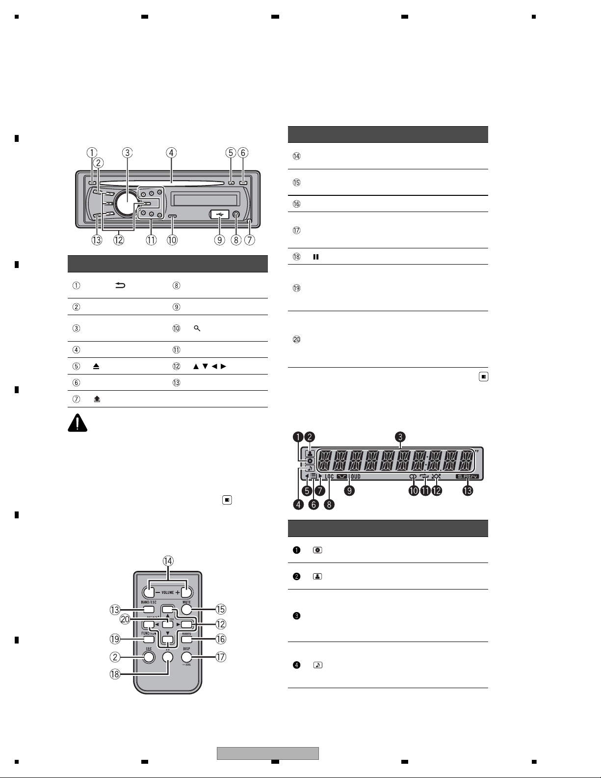
2.3 PANEL FACILITIES
Head unit
traPtraP
DISP/ / SCRL
AUX input jack (3.5
mm stereo jack)
SRC / OFF USB port
MULTI-CONTROL
(M.C.)
(list)
Disc loading slot 1 to 6
(eject) / / /
CLOCK BAND/ ESC
(detach)
CAUTION
Use an optional Pioneer USB cable (CD-U50E) to
connect the USB audio player/USB memory to
the USB port. Since the USB audio player/USB
memory is projected forward from the unit, it is
dangerous to connect directly.
Do not use the unauthorized product.
Remote control
Part Operation
VOLUME
Press to increase or decrease volume.
MUTE
Press to mute. Press again to unmute.
AUDIO Press to select an audio function.
DISP/ SCRL
Press to select different displays.
Press and hold to scroll through
the text information.
Press to pause or resume.
FUNCTION
Press to select functions.
Press and hold to recall the initial
setting menu when the sources
are off.
LIST /
ENTER
Press to display the disc title,
track title, folder, or file list depending on the source.
While in the operating menu,
press to control functions.
Display indication
Indicator State
(disc)
The disc (album) name is displayed.
(artist)
The disc (track) artist name is displayed.
Main display section
• Tuner: band and frequency
• Built-in CD player and USB:
elapsed playback time and
text information
(song)
The track (song) name is displayed.
A playable audio file has been selected while operating the list.
8
DEH-22UB/XSUC
5 678
56
7
8
C
D
F
A
B
E
An upper tier of folder or menu
exists.
(folder) The list function is operated.
A lower tier of folder or menu exists.
LOC The local seek tuning is on.
LOUD
(loudness)
The loudness is on.
(stereo)
The selected frequency is being
broadcasted in stereo.
(repeat) Track or folder repeat is on.
(ran-
dom)
Random play is on.
(sound retriever)
The sound retriever function is
on.
DEH-22UB/XSUC
9
1234
1234
C
D
F
A
B
E
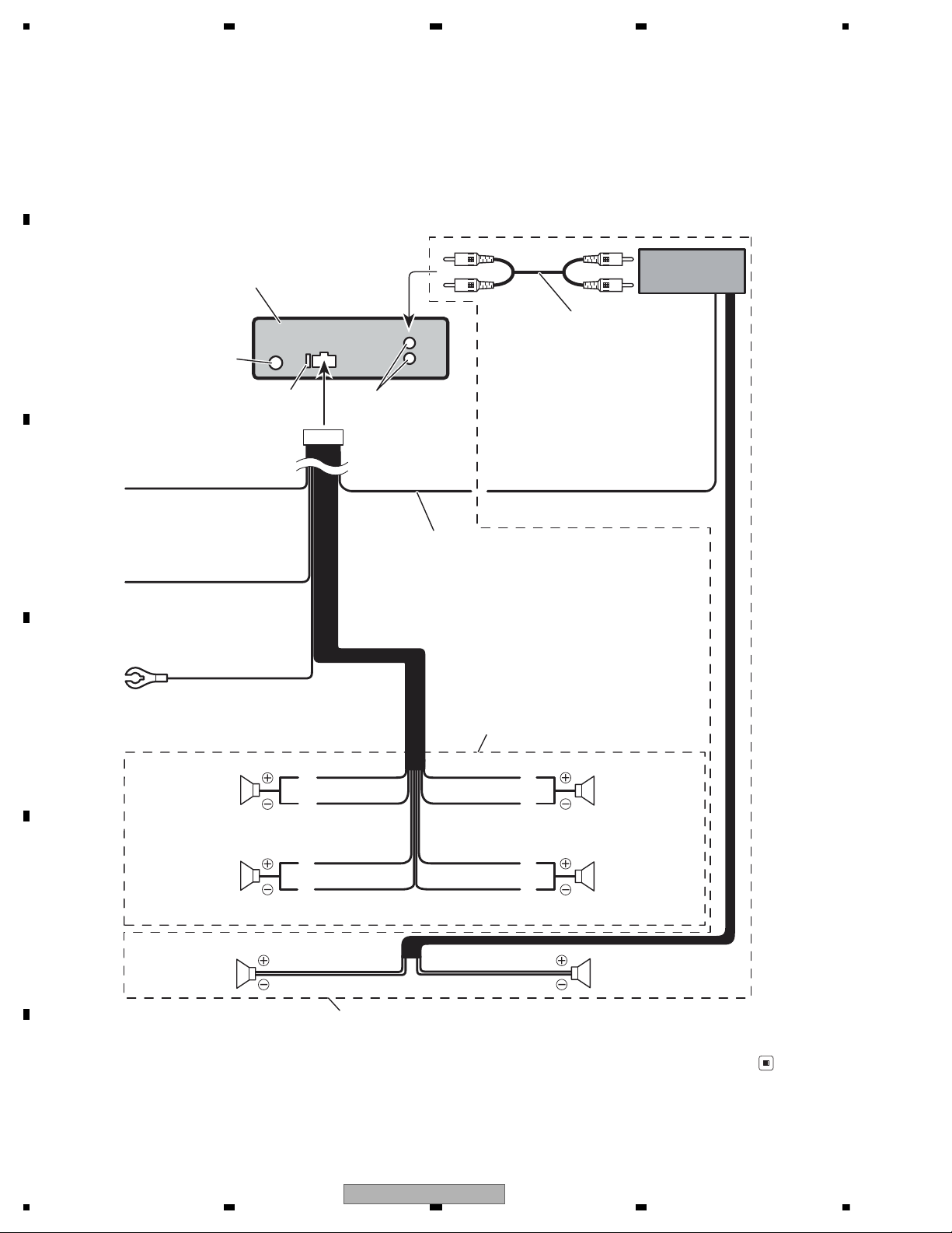
2.4 CONNECTION DIAGRAM
Connection diagram
Connect with RCA cables
(sold separately)
Rear output
This product
Antenna jack
Fuse (10 A)
Blue/white
Connect to system control terminal of the
power amp or auto-antenna relay control
terminal (max. 300 mA 12 V DC).
Yellow
Connect to the constant 12 V
supply terminal.
Red
Connect to terminal controlled
by ignition switch (12 V DC).
Black (chassis ground)
Connect to a clean, paint-free
metal location.
Power amp
(sold separately)
System remote control
Left Right
Perform these connections when using
the optional amplifier.
rekaepsraeRrekaepsraeR
White/black
Violet/black
Violet
With a 2 speaker system, do not connect
anything to the speaker leads that are not
connected to speakers.
rekaepstnorFrekaepstnorF
White
Gray/black
Gray
Green/black
Green
rekaepsraeRrekaepsraeR
10
DEH-22UB/XSUC
5 678
56
7
8
C
D
F
A
B
E
demrifnocebotmetIserudecorP.oN
1 Confirm whether the customer complain has
been solved.
If the customer complain occurs with the
specific media, use it for the operation check.
The customer complain must not be
reappeared.
Display, audio and operations must be
normal.
2 CD Play back a CD.
(Track search)
No malfunction on display, audio and
operation.
3 FM/AM tuner Check FM/AM tuner action.
(Seek, Preset)
Switch band to check both FM and AM.
Display, audio and operations must be
normal.
4 Check whether no disc is inside the product. The media used for the operating check must
be ejected.
retfaecnaraeppastinotridrosehctarcsoNkcehcecnaraeppA5
receiving it for service.
Item to be checked regarding audio
3. BASIC ITEMS FOR SERVICE
3.1 CHECK POINTS AFTER SERVICING
To keep the product quality after servicing, please confirm following check points.
See the table below for the items to be checked regarding audio:
Distortion
Noise
Volume too low
Volume too high
Volume fluctuating
Sound interrupted
3.2 PCB LOCATIONS
CD Core Unit (S11USB)
C
Keyboard Unit
B
Unit Number : YWM5449
Unit Name : Tuner Amp Unit
Unit Number :
Unit Name : Keyboard Unit
Unit Number : CWX3776
Unit Name : CD Core Unit(S11USB)
Tuner Amp Unit
A
DEH-22UB/XSUC
11
1234
1234
C
D
F
A
B
E
3.3 JIGS LIST
- Jigs List
Name
Test Disc
L.P.F.
Jig No.
TCD-782
Remarks
Checking the grating
Checking the grating (Two pieces)
Name
Jig
- Grease List
Name
Grease
Grease
Grease No.
GEM1024
GEM1045
Remarks
CD Mechanism Module
CD Mechanism Module
e
Before shipping out the product, be sure to clean the
following portions by using the prescribed cleaning
tools:
Portions to be cleaned Cleaning tools
CD pickup lenses Cleaning liquid : GEM1004
Cleaning paper : GED-008
m
3.4 CLEANING
No.
rease No.
emarks
emarks
12
DEH-22UB/XSUC

5 678
56
7
8
C
D
F
A
B
E
DEH-22UB/XSUC
13
1234
1234
C
D
F
A
B
E
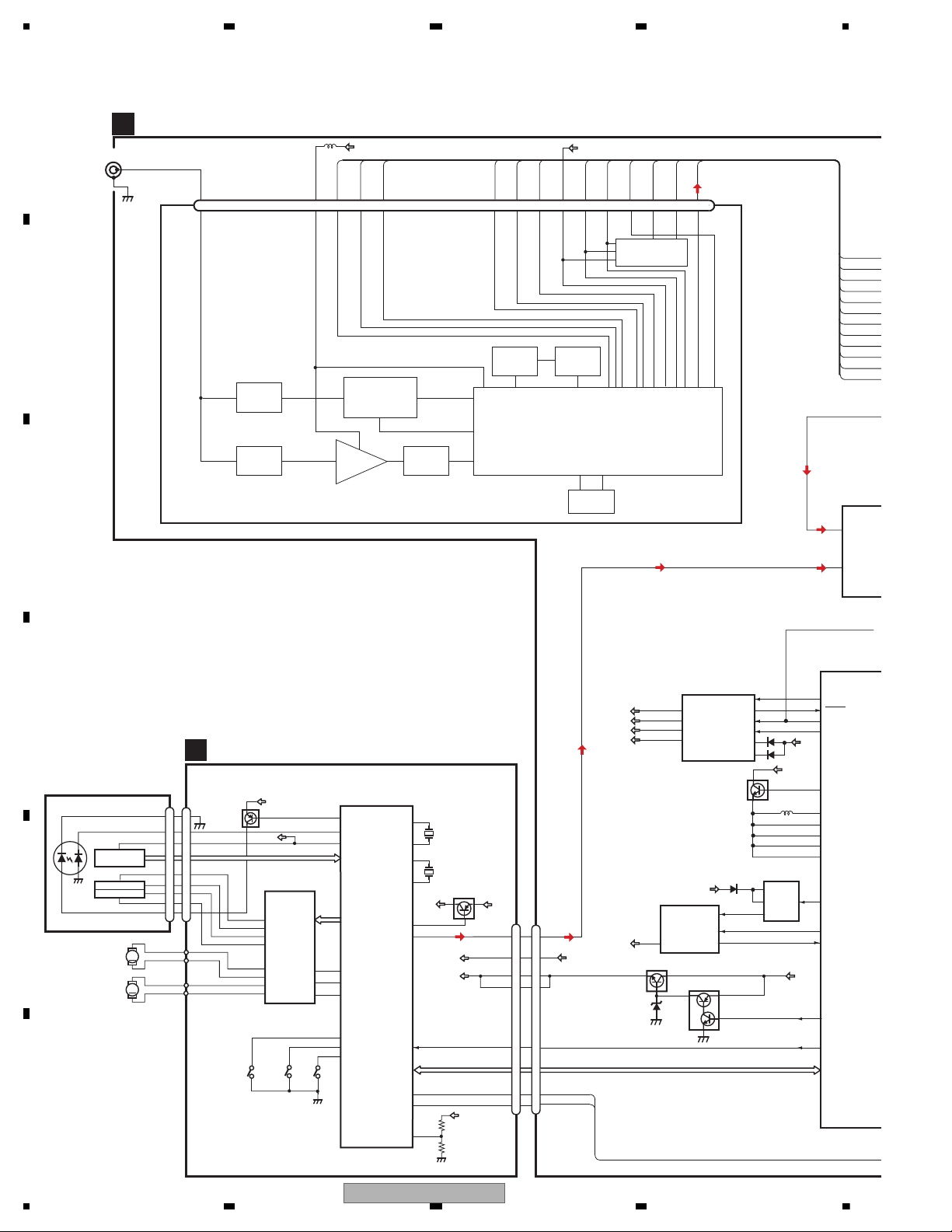
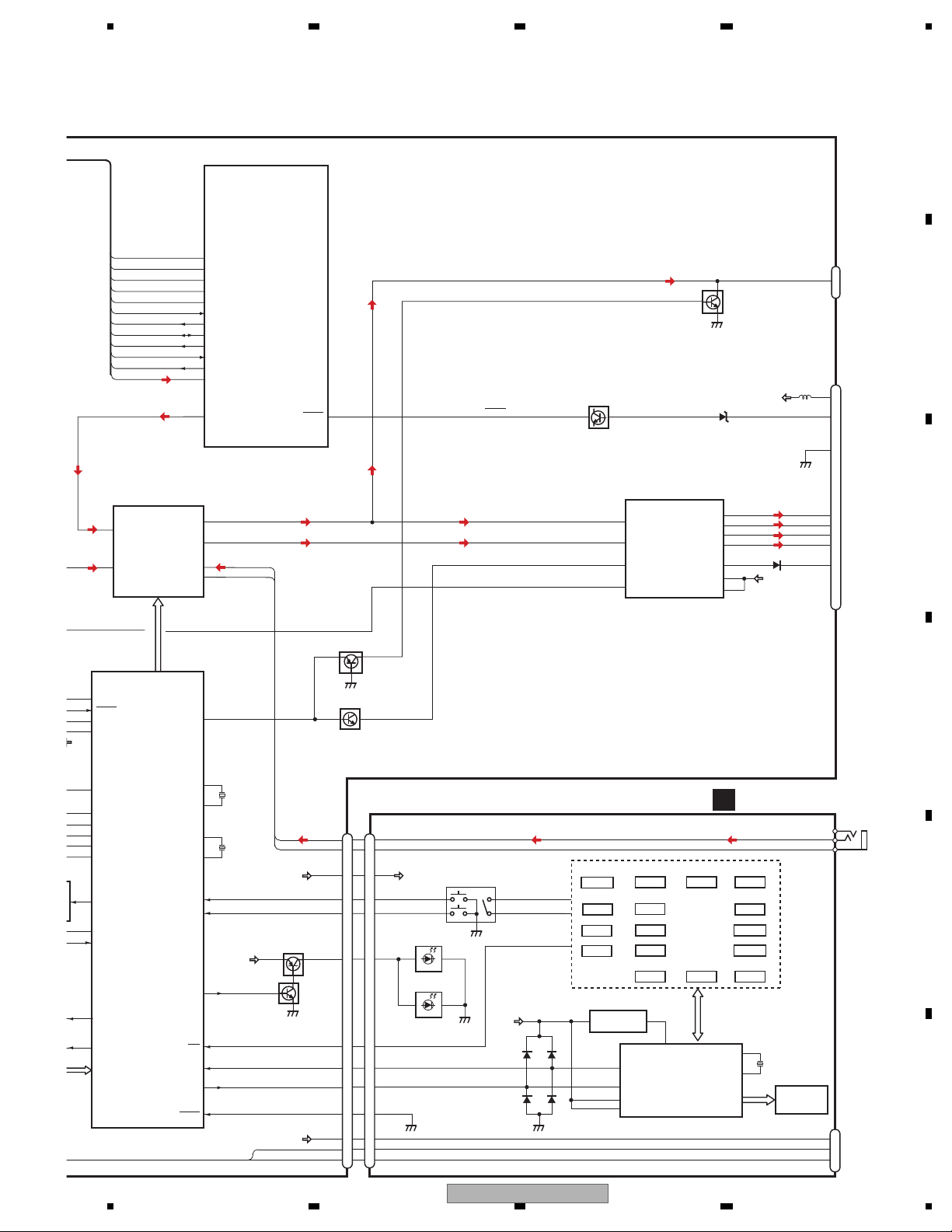
4. BLOCK DIAGRAM
PICKUP UNIT
(P10.5)(SERVICE)
CD CORE UNIT(S11USB)
C
BRST,BRXEN,BSRQ
CN701
Q101
M
LD
MD
S903
DSCSNS
SPINDLE
MOTOR
M
LOADING/CARRIAGE
MOTOR
LD-
MD
15
5
HOLOGRAM
UNIT
IC301
BA5839FP
IC201
PE5715A
RF AMP, CD DECODER, MP3&WMA DECODER
DIGITAL SERVO/DATA•PROCESSOR
CPU, USB HOST CONTROLLER
ACTUATOR/
MOTOR DRIVER
2
VD
VD
13
LOUT
9
CN101
16
SOP
15
SOM
18
LCOP
17
LCOM
21
CLCONT
55
LOUT
9
CONT
TD,FD
AC,BD,E,F
SD,MD
S901
HOME
S905
8EJ
LD+
14
141
LD
142
PD
CONT
CLCONT
HOME
9
20
41
VDD
1
VDD
BDATA,BSCK
VDD
15
5
FOCUS ACT.
TRACKING ACT.
FOP
TOP
2
1
TOP
FOP
11
FOP
14
TOP
2
1
14
8EJ
7
DSCSNS
10
16
/RESET
8
/RESET
88
VREF
REFO
133
REFOUT
33
FOM
FOM
12
FOM
44
TOM
TOM
13
TOM
22
LOEJ
LOEJ
28
52
50
X201
XTAL
/XTAL
16.93MHz
VDSENS
11
VD
16
17
DP
DM
4
5
DM
DP
2
1
X205
48MHz
USBXTAL
/USBXTAL
Q102
39
/PUEN
VCC
VDD
IN2_L
IN1_L
2
IC
PML
ELECTRON
SOURCE
TUNL
1
ANT401
1
2
CN651
TUNER AMP UNIT
VCK, VDT, VST
LOUT
A
SYS+B
ANTENNA
IFA
IFB
7
VDD3V
11
SWVDD3V
SW5V
6
5
BSENS
SYSPW
PWROFF
2
1
36
47
15
SWVDD
4
1
BRST,BRXEN,BSRQ,BDATA,BSCK
CDRESET
12
4
3
RESET
16
FM/AM TUNER UNIT
ANT
SL-IN
REFA
REFB
LDET
SWVDD3V
DI
CK
CE1
DO
CE2
SLOUT
SL-IN
IFA
IFB
REFA
REFB
LDET
DI
CK
CE1
DO
CE2
SLOUT
CD-Lch
3
REGULATOR IC
IC911
BA49181-V12
B.UP
10
9
VDD3V
SYS+B
SWVDD
VDD
SW5V
SYS+B
BESNS
SW5VCONT
+B
IC501
BD9007F
USB5V
IC712
BD6538G
PVin
Vin
SW
EN
VIN
EN
FLG
+B.UP
VDDCONT
SYSPW
8
7
USB5V
VOUT
5
SYSTEM
COMP
DREG
85
SYNC
USBCTL
FLG
255
2
8
1
28
1
3
27
4
SWVDD3V
Q601
PLL_VDD
DVDD3
M-REGC
55
9
57
DVDD2
94
DVDD4
121
B.UP
5
Q751
18
19
Q752
VDCONT
126
CD VD
VD
B.UP
USDP
USDM
ATT
ATT
TANK
ATT RF
LFP
LFPVCO
CF
IC1
MIX / IF / PLL
IC2
EEPROM
1 2 3 4 5 6 7 8 9 10 12 13 14 15 16 17 18 19 2011
ANT
VCC
SLIN
IFOUTA
IFOUTB
DGND
REFINA
REFINB
LDET
VDD
DI
CK
CE1
DO
CE2
SLOUT
RFGND1
RFGND2
RFGND3
RFGND4
VDD
IC60
PN5
14
DEH-22UB/XSUC
5 678
56
7
8
C
D
F
A
B
E
IN2_L
IN1_L
2
IC201
PML014B
ELECTRONIC VOLUME/
SOURCE SELECTOR
TUNL
1
7
Rear_L
B.UP
35
44
MUTE
9
7
3
5
FL-
VCC
VCC
FL+
RL-
RL+
FL-
FL+
RL-
RL+
BREM
ACC
GND
22
AMP
IC301
PAL007E
Q921
MUTE
CN832
VCK, VDT, VST
Q351(1/2)
Q351(2/2)
B.UP
Q801
SYSTEM MICRO
COMPUTER
ASENSE
13
7
5
1
3
18
16
JA901
12
11
17
6
19
SOURCE
ROT1
ILM+B
DPDT
KYDT
SRC
33
111
ILMPW
2
DPDT
23
KYDT
24
CN251
RLIn
12
ROT1
4
ROT0
110
ROT0
Q802
20
DSENS
USB5V
DSENS
34
16
14
DM
DP
ASENS
6
Front_L
FLIn
11
XOUT
XIN
82
X601
74.1MHz
81
BU_X1
BU_X2
52
X681
4.7186MHz
51
Q251
MUTE
20
6
25
B.REM
ASENS
RL
14
BSENS
SYSPW
PWROFF
36
47
15
SWVDD
1
CDRESET
16
SL
62
SL-IN
IF_INA
77
IFA
IF_INB
78
IFB
FREFA
96
REFA
FREFB
97
REFB
LOCK
99
LDET
TUNDO
100
DI
TUNCK
101
CK
TUNDI
102
CE1
CE2
CE
103
DO
SL
109
CE2
136
SLOUT
2
B.UP
RCA OUT
POWER
CONNECTOR
L_OUT
59
CD-Lch
B.UP
SYSTEM MICRO
COMPUTER
4
STBY
B.UP
3
SW5V
18
USB5V
USDP
USDM
AUX-G
5
AUX-L
7
AUX-L
4
AUX-G
5
IN4+_L
IN4-_L
ILMPW
DREG
85
SYNC
USBCTL
FLG
255
28
27
PLL_VDD
DVDD3
M-REGC
55
9
57
DVDD2
94
DVDD4
121
MUTE
B.UP
VDCONT
126
IC601(2/2)
PN5034A
IC601(1/2)
PN5034A
IC1802
GP1UXC14RK
REMOTE CONTROL
SENSOR
17
3
VCC
1
REM
DPDT
DM
DP
USB5V
DM
DP
USB5V
KDT0-3
KST0-4
LCD1801
CN1821
CN1901
CN1911
FRONT
AUX
USB
KEYBOARD UNIT
18
18
KYDT
19
20
B
14
16
SW5V
SW5V
17
22
X1801
5.00MHz
23
KEY MATRIX
S1837
S1845
BAND/ESC
4
S1836
S1835
S1825
S1826
S1827
S1828
S1829
S1830
S1823
S1824
S1831
S1832
S1833
S1834
S1821
S1822
10
56
1
3
2
4
6
1
2
4
5
3
3
ILM+B
ILLUMI
D1852-D1857
D1861-D1870
LCDBK
D1851
12
DSENS
20
UP
LEFT
RIGHT
DOWN
S1843
S1844
CD EJECT
REGION
DISP/BACK
SRC
LIST
6
5
S1840
3
S1839
S1841 S1842
S1838
1
2
AUX L
7
AUX G
AUX L
AUX R
AUX G
ROT1
ROT0
KST1
KDT2
AUXV/SOURCE
5
SOURCE
11
2
3
1
LCD DRIVER/
KEY CONTROLLER
IC1801
PD6340A
KEY DATA
DPDT
KYDT
X0
X1
VLCD
VDD
REM
DEH-22UB/XSUC
15
1234
1234
C
D
F
A
B
E
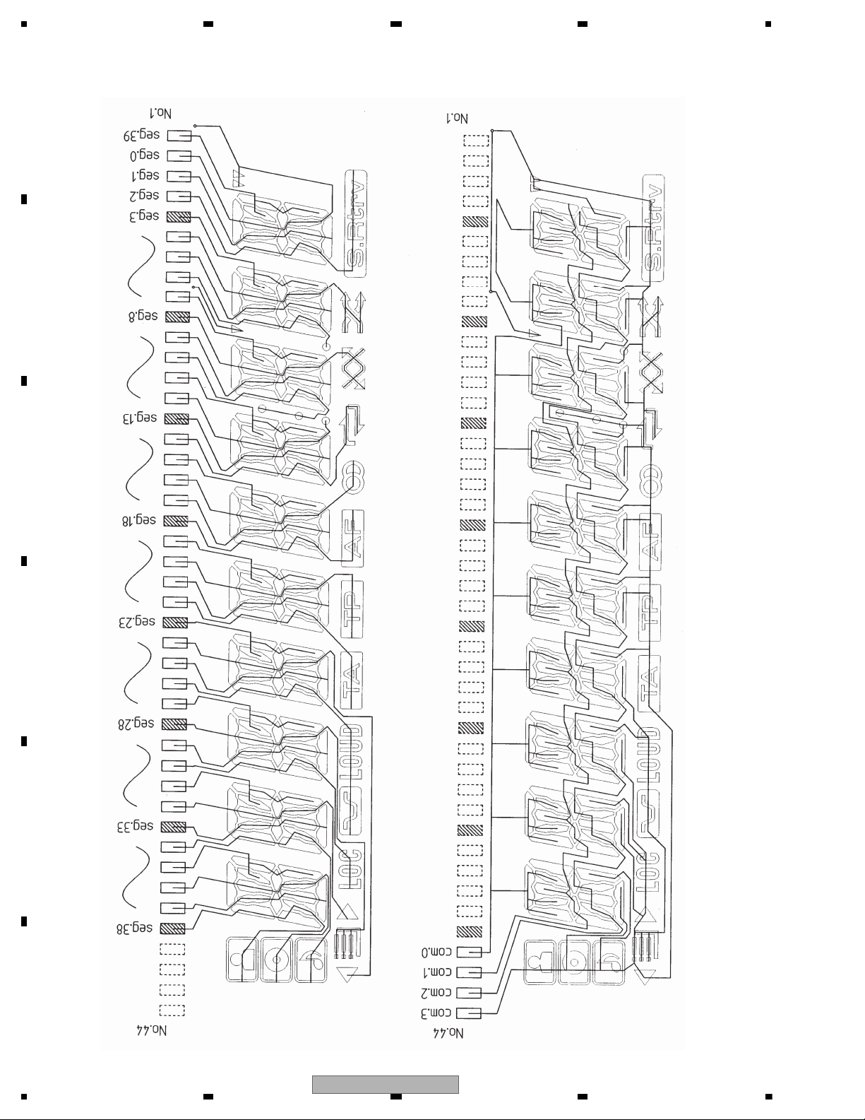
SEGMENT
COMMON
LCD (CAW1970)
16
DEH-22UB/XSUC
5 678
56
7
8
C
D
F
A
B
E
VDD = 3.3 V
Pin 8
BSENS
Pin 36
ASENS
Pin 35
BSENS = L
Starts
communication
with Grille
microcomputer.
SWVDD <- H
Pin 1
Source keys
operative
Source ON
SYSPW <- H
Pin 15
300 ms
300 ms
Completes power-on operation.
(After that, proceed to each source operation)
In case of the above signal, the communication
with Grille microcomputer may fail.
If the time interval is not 300 msec, the oscillator
may be defective.
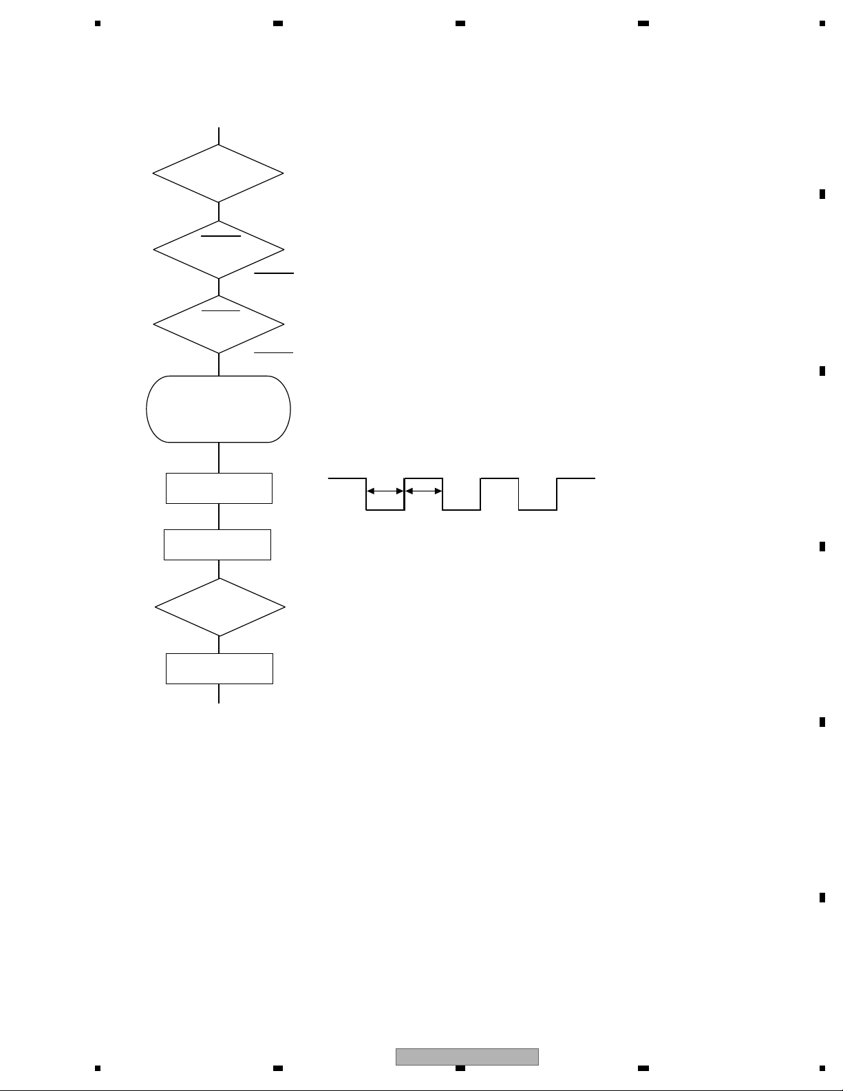
Power ON
ASENS = L
5. DIAGNOSIS
5.1 OPERATIONAL FLOWCHART
DEH-22UB/XSUC
17

1234
1234
C
D
F
A
B
E
5.2 ERROR CODE LIST
8-digit display 6-digit display 4-digit display
ERROR-xx ERR-xx E-xx
(2) LIST OF CD ERROR CODES (Error Mode: 0xFD)
Code Classification
Error code to be displayed
Details and possible causes
10
Electricity Carriage Home NG
Failure in communication with the Servo LSI
The CRG cannot move toward the inner track.
The CRG cannot move from the inner track.
--> Defective HOME SW; Failure in CRG movement; Failure in communication between
the microcomputer and the Servo LSI.
11
Electricity Focus Search NG Focusing not available
--> Disc placed upside-down; CD-RW disc used; Stains on the disc; excessive vibration.
23 Disc File Format NG Data are written in a file format not supported.
--> A CD-ROM disc on which data are written in a file format other than ISO 9660,
Level-1 or -2 (for example, in UDF) is loaded.
22 Disc No playback Playable MP3 or WMA file not found
--> No MP3 or WMA file exists on the loaded CD-ROM disc.
24
Disc All DRM All the playable files on the disc are DRM-protected.
--> This error code will not be displayed when even one file not protected by DRM is
contained on the disc.
17 Electricity Setup NG AGC protection does not work. Focus can be easily lost.
--> Scratches or stains on the disc; excessive vibration; CD-RW disc used.
15
Electricity Failure in RF data RF not read
--> A CD-R disc that does not contain data loaded
--> A CD-RW disc that does not contain data loaded
12
Electricity Spindle Lock NG
Subcode NG
RF-amp NG
Spindle not locked. Subcode not readable.
Proper RF AMP gain not obtained.
--> Defective spindle; Scratches or stains on the disc; excessive vibration.
-->
A CD-R disc that does not contain data loaded, or in a rare case, disc placed upside-down.
--> CD signal error.
30
Electricity Search Time Out Failed to reach a target address
--> CRG tracking error or scratches on the disc
50 Mechanism Failure in ejection Disc ejection not completed
--> A foreign object inserted in the mechanism; Disc jammed.
51
Mechanism Failure in retried
turning for ejection
Disc could not be ejected even after disc turning had been retried.
--> A foreign object inserted in the mechanism; Disc jammed.
52
Mechanism Failure in disc loading Disc loading not completed
--> A foreign object inserted in the mechanism; Disc jammed.
NOTES
• Indications of error codes are available only during disc operations, because CD operations are
unavailable if a mechanical error is generated.
• If the TOC cannot be read, this is not processed as an error, and operation continues accordingly.
• If you design a new head unit, be sure to use one of the display formats indicated in “Display example of
the head unit.”
ERROR CODES
(1) DISPLAY METHOD
If “0xFD” error mode is displayed in CD MODE (CD MODE area for display) or USB MODE (USB MODE area), an error code
will be displayed in the DMIN (minute display) and DSEC (second display) areas.
The same code is displayed in the DMIN and DSEC areas.
The DTNO area is blank (#0FFH), as it conventionally was.
• The error mode for a VD error is 0xFB. (This is because the system microcomputer recognizes a VD error even in the No
Display format.)
• Display example of the head unit
Depending on the display capability of LCDs, the display format varies, as shown below. XX denotes an error number.
Note: In a case of an OEM product, the error display format is subject to the specifications used by the equipment
manufacturer.
If a CD or USB memory device is inoperable, or operation of such media is stopped by an error, the error mode is established
and a cause of the error is displayed by an error code. Indication of error codes is intended to reduce the number of calls from
customers and facilitate failure analysis and repair work in servicing.
18
DEH-22UB/XSUC

5 678
56
7
8
C
D
F
A
B
E
(3) USB-RELATED ERROR CODES
16
(*1)
Device iPod authentication error Authentication of iPod failed
--> After a reattempt of iPod authentication, an error was returned from the iPod machine
and authentication IC.
18
Device Unsupported device Connection of a device not supported was detected.
--> A device other than a mass-storage device and iPod is connected.
--> An iPod of a generation earlier than 5G/nano is connected. Or, an iPod (even one of a
generation after 5G/nano) with the firmware that does not support digital streaming is
connected.
24
Device All DRM
*Error code only for models that support iPod.
Note: Whether power supply failed or not can be judged from just the error mode (0xFA). (Referring to the error code [0xA1] is not necessary.)
23 Device File Format NG Data are written in file format not supported.
--> A format other than FAT is used.
22
Device Playback unavailable Playable file (MP3/WMA/AAC/WAV) not found
--> No playable file (MP3/WMA/AAC/WAV) exists in the device set.
19
Device Communication error Communication with a device failed.
--> Communication failed because of a defective device, etc.
(4) LIST OF ERROR CODES (Error Mode: 0xFA) Only for USB
A1 System Failure in power supply
Excess current detected in the USB bus.
--> Electric current exceeding the specified 500 mA flowed in the USB bus.
The bus power is shut off and the unit is stopped in response to an error.
For restoration, turn the unit OFF then back ON again
Note: Whether power supply failed or not can be judged from just the error mode (0xFB). (Referring to the error code [0xA0] is not necessary.)
(5) LIST OF ERROR CODES (Error Mode: 0xFB) Only for CD
A0 System Failure in power supply A voltage or ground short was generated in the VD power.
--> Defective SW transistor; Failure in the power supply unit (defective connector);
Ejection is not possible; Restoration is only possible by turning the unit OFF then
back ON again.
• The 2 high-order digits of an error code denote the main
classification, shown below.
1x: Setup-related errors
2x: Errors related to TOC reading
3x: Search-related errors
4x: Playback-related errors
5x: Loading-ejection-related errors
Ax: Other type of errors
• How to restore from each error is shown below.
1x, 2x, 3x, and 4x: ACC-OFF then ON, CD-OFF then ON,
Disc ejection, DKSTOP then DKPLAY
5X: ACC-OFF then ON, Disc ejection, Disc reloading,
Disc removal
Ax: ACC-OFF then ON
NOTES
• The 2 high-order digits of an error code denote the main
classification, shown below.
1x: Setup-related errors
2x: Errors related to file-system reading
Ax: Other type of errors
• How to restore from each error is shown below.
1x: ACC-OFF then ON, USB-OFF then ON, Device removal,
DKSTOP then DKPLAY
2X: ACC-OFF then ON, USB-OFF then ON, Device removal,
DKSTOP then DKPLAY
Ax: ACC-OFF then ON
(6) ACTIONS OF CD/USB DURING ERROR
Mode Error code CD action USB action Mode Error code CD action USB action
3x
Stopped for an error
Stopped for an error
Stopped for an error
Stopped for an error
Stopped for an error
Stopped for an error
Stopped for an error
Stopped for an errorOperable
Operable
Operable
Operable
Operable
Operable
Operable
Operable
2x (CD)
2x (USB)
FD
FD
FB
FA
1x
4x
5x
A0
A1
Code Classification
Error code to be displayed
Details and possible causes
Code Classification
Error code to be displayed
Details and possible causes
Code Classification
Error code to be displayed
Details and possible causes
All the playable files on the disc are DRM-protected.
--> This error code will not be displayed when even one file not protected by DRM is
contained on the disc.
DEH-22UB/XSUC
19
1234
1234
C
D
F
A
B
E
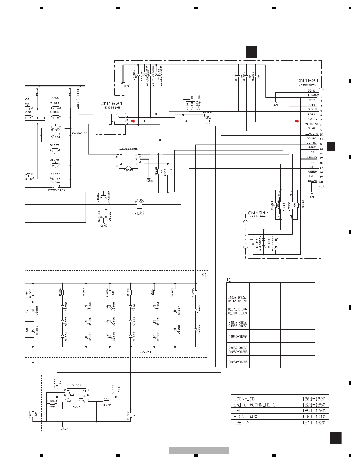
5.3 CONNECTOR FUNCTION DESCRIPTION
REAR
OUTPUT
ANTENNA
1 FL+
2 FR+
3 FL4 FR5 RL+
6 RR+
7 RL8 RR-
9 TEL
10 NC
11 NC
12 NC
13 ACC
14 B.REM
15 B.UP
16 GND
16
14
12
10 8
6
42
15
13
11
9 7
5
31
20
DEH-22UB/XSUC

5 678
56
7
8
C
D
F
A
B
E
1. To enter the test mode (1)
Turn on ACC and Backup while pressing the RIGHT and the DOWN buttons together.
2. Operation method
V E R # # # #
N O E E P R O M
S U M E R R O R
S S S S C C C C
1
2
3
4
1
2
3
4
.
Key
LIST
1
4
5
6
DISP
Contents
All lighting of display
All lights out of display
LCD check mode A
LCD check mode B
LCD check mode C
System version display
ex.) Ver.7.01 -> “VER 7.01”
3. To enter the test mode (2)
Turn on ACC and Backup while pressing the 1 and the 3 buttons together.
4. Operation method
Start to test mode
ROM Correction version display
ROM Correction is not connected
ROM Correction check sum error
Normal movement
Normal display
The display mode to the display usually.
Display stop
To the static display of the display mode.
[Test Overview]
Change display as follows by pressing the 1 and the 3 buttons together.
Sn ROM Correction number
Cn CH use information (1:Use / 0:Not use Corresponds from the left to CH1, CH2, CH3, CH4)
6. SERVICE MODE
6.1 DISPLAY TEST MODE
DEH-22UB/XSUC
21

1234
1234
C
D
F
A
B
E
6.2 CD TEST MODE
[Key]
Contents
Display
[BAND]
Power On
(T.Offset is adjusted)
TRK MIN SEC
00 00 00
[3]
Power On
(T.Offset is not adjusted)
99 99 99
[2]
RF AMP
Gain switching
GG GG GG
*1
[4]
SPINDLE
Speed switching
SP SP SP
*9
[3]
Focus Close
S curve check
TRK MIN SEC
91 91 91
[6]
Focus Mode switching
0X 0X 0X
*2
[1]
Tracking Servo
Close
00 00 00
or 99 99 99
[<]
CRG +
[2]
Self-adjusting
switching
TRK MIN SEC
?? ?? ??
*3*8
[>]
CRG -
*8
[BAND]
Power Off
TRK MIN SEC
[BAND]
Power Off
TRK MIN SEC
[BAND]
Power Off
TRK MIN SEC
[BAND]
Power Off
TRK MIN SEC
[1]
T.Close & AGC
Applicable servomechanism
TRK MIN SEC
?tr ?min ?sec
[6] [3]
RF AGC /
RF AGC coefficient display
[<]
CRG +
8X 8X 8X
or 9X 9X 9X
[2]
T.Balance adjustment /
T.BAL coefficient display
TRK MIN SEC
?? ?? ??
[>]
CRG -T.Close
Applicable servomechanism
?? ?? ??
[1]
F,T,RF AGC
F.Bias display switching
TRK MIN SEC
TRK MIN SEC
TRK MIN SEC
TRK MIN SEC
?tr ?min ?sec
TRK MIN SEC
[3] [6]
CRG/TR jump
value switching
[<]
CRG/TR Jump +
[2]
Tracking Open
[>]
CRG/TR Jump -
?tr ?min ?sec
TRK MIN SEC
TRK MIN SEC
TRK MIN SEC
?tr ?min ?sec
00 00 00
or 99 99 99
TRK MIN SEC
TRK MIN SEC
?tr ?min ?sec
8X 8X 8X
or 9X 9X 9X
8X 8X 8X
or 9X 9X 9X
00 00 00
or 99 99 99
TRK MIN SEC
?tr ?min ?sec?? ?? ??
*7
F,T AGC / F.Bias
RF AGC
8X 8X 8X
or 9X 9X 9X
[2]
Tracking Open
*6
*5
*4 *4
Operation
[Key]
Test Mode
[BAND] Power On/Off
[<]
CRG + / TR Jump +
(Direction of the external surface)
[>]
CRG - / TR Jump (Direction of the internal surface)
[1] T. CLS & AGC & Applicable servomechanism /
AGC,AGC display setting
[2] RF Gain switching / Offset adjustment display /
T.Balance adjustment / T. Open
[3] F. Close,S. Curve / Rough Servo and RF AGC /
F,T,RF AGC
[4]
SPDL 1X/2X switching
As for the double speed(2x), audio output cannot be
supported.
[5]
Gop Mode switching
[6] F. Mode switching / Tracking Close / CRG TR
Jump Switching
*) After the [EJECT] key is pressed keys other than the [EJECT] key should not be pressed, until disc ejection is complete.
When the key [2] or [3] is pressed during the Focus Search, the power supply should be immediately turned off (otherwise the lens
sticks to Wall, causing the actuator to be damaged).
In the case of TR jump other than to 100TR, the function shall continue to be processed even if the TR jump key is released. As for
the CRG Move and 100TR Jump, the mechanism shall be set to the Tracking Close mode when the key is released.
When the power is turned on/off the jump mode is reset to the Single TR (91) while the gain of the RFAMP is reset to 0 dB. At the
same time all the self-adjusting values shall return to the default setting.
*10
TRK MIN SEC
[5]
Gop Mode
Gop Mode switching
OL OL OL
- Flow Chart
[CD] or [SOURCE]
Source ON
TRK MIN
[4] + [6] + Reset
Test Mode IN
*1) TYP t + 6 dB t + 12 dB
TRK
MIN
SEC
TRK06MIN06SEC
06
TRK12MIN12SEC
12
*2) Focus Close
t S. Curve t F EQ measurement setting
TRK00MIN00SEC
00
TRK
01
MIN01SEC
01
TRK02MIN02SEC
02
(
TRK99MIN99SEC
99)
*3) F.Offset Display t T.Offset Display t Switch to the
order of the original display
*4) 1TR/4TR/10TR/32TR/100TR
*5) Single
t 4TR t 10TR t 32TR t 100TR t CRG Move
9x(8x):91(81) 92(82) 93(84) 94(84) 95(85) 96(86)
*6) Only at the time of CRG move, 100TR jump
*7) TRK/MIN/SEC
t F.AGC t T.AGC Gain t F.Bias t RF AGC
*8) CRG motor voltage = 2 [V]
*9) TYP (1X)
t 2X t 1X
TRK
MIN
SEC
TRK
22
MIN22SEC
22
TRK11MIN11SEC
11
*10) OFF(TYP)
t FORCUS t TRACKING
TRK
MIN
SEC
TRK
70
MIN70SEC
70
TRK71MIN71SEC
71
As for the double speed (2x), audio output cannot be supported
Do not do Tracking Servo Close before doing Focus Servo Close. (Because the overcurrent flows)
22
DEH-22UB/XSUC

5 678
56
7
8
C
D
F
A
B
E
1
1
2
2
3
4
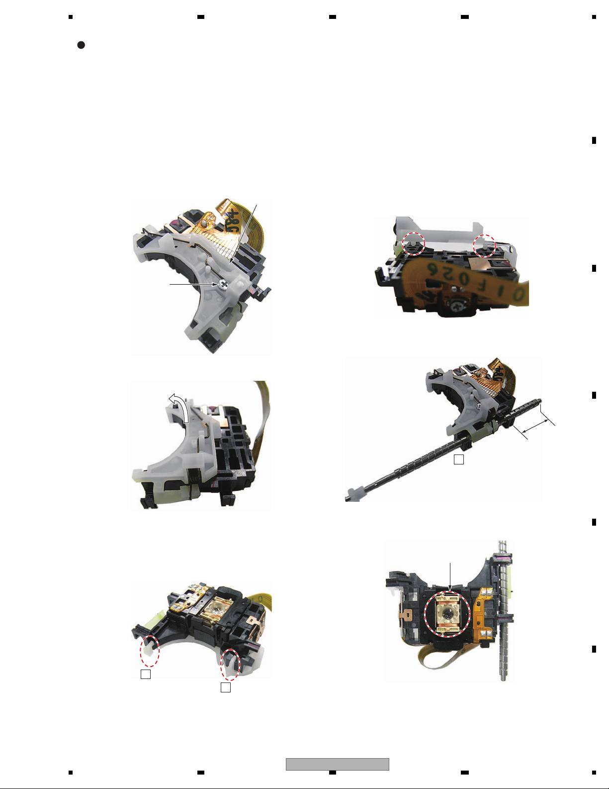
While the photograph shown is slightly different from this model in shape, the disassembly procedure is the same.
-
Removing the Case and Panel Assy (Fig.1)
Remove the Case.
-
Removing the CD Mechanism Module (Fig.2)
Remove the four screws.
Disconnect the FFC
and then remove the CD Mechanism Module.
Fig.1
Fig.3
Removing the Tuner Amp Unit (Fig.2, 3)
Fig.4
Remove the two hooks
and then remove the Panel Assy.
1
Fig.2
Remove the two screws.(Fig.3)
Remove the two screws
and then remove the Tuner Amp Unit.(Fig.4)
Straighten the tabs
at two locations indicated.(Fig.4)
Remove the two screws.(Fig.4)
1
1
1
1
2
CD Mechanism Module
Panel Assy
Case
1
1
1
Tuner Amp Unit
1
2
2
3
3
4
4
7. DISASSEMBLY
DEH-22UB/XSUC
23

1234
1234
C
D
F
A
B
E
1. Hold the Upper and Lower Frames at the specified parts (circled with broken blue lines in the photo below).
2. You can hold the tabs of the Lower Frame (circled with broken green lines in the photo below) if you do so only while lifting
the Mechanism Unit from the table. Keeping the Mechanism Unit lifted by holding these tabs with your fingers may result in
deformation.
3. Be careful NOT to hold the front part of the Upper Frame or the CRG Mechanism and NOT to insert foreign objects into
these mechanisms. Doing so may result in deformation.
Proper handling
Improper handling
How to Hold the Mechanism Unit
24
DEH-22UB/XSUC

5 678
56
7
8
C
D
F
A
B
E
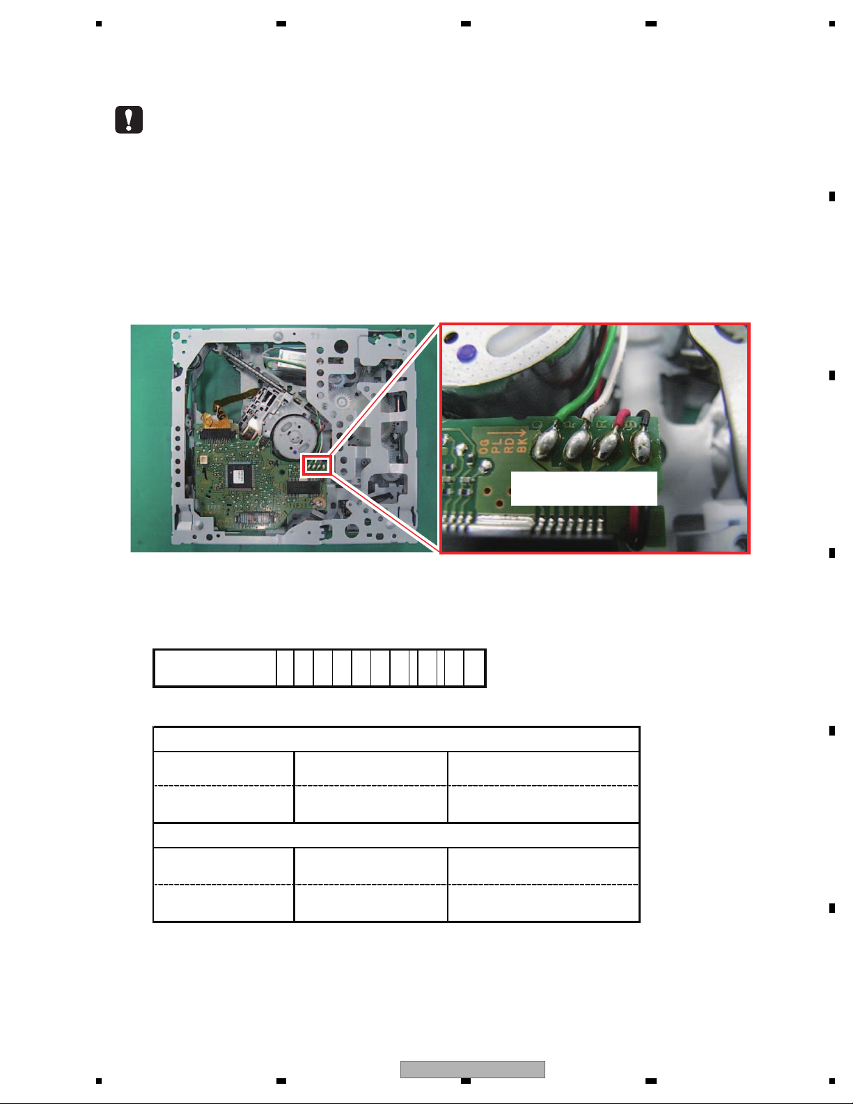
1. Remove the solder from the CRG-motor lead wire (Fig. 1).
2. Push in the Disc Detection Arm while applying 4-V power to the CRG Motor (Fig. 2). (Apply 4-V power to the green lead
wire. The white lead wire is for grounding.)
The Mechanism Module is set to the clamped state, and the PU will move toward the outer track.
Note: NEVER apply power to the CRG-motor lead wire without removing the solder from the wire. Doing so may result in
damage to the ICs and the PU.
3. Stop the motor when the PU reaches around the middle track.
Note: Jumpiness will occur when the PU reaches the outermost track. Although jumpiness does not constitute a problem,
it is recommended that it occur as least frequently as possible.
Fig. 1
Note: Be aware that the colors of the lead wires do not match the
indications on the Core Board Pattern (green wire to O and
white wire to P).
Fig. 2
Disc Detection Arm
Mechanism Module: How to Set to the Quasi-Clamp State (Driven by the Motor)
DEH-22UB/XSUC
25

1234
1234
C
D
F
A
B
E
How to Remove the PU Unit
How to Move the PU toward the Outer Track
1. Set the unit to the quasi-clamp state, following the procedures described in “Mechanism Module: How to Set to the Quasi Clamp State (Driven by the Motor).”
2. Temporarily change the engagement position of the bias spring of the feed screw (Fig. 2b).
Be careful not to cut yourself on the tip of the spring.
3. Hold the PU unit by parts A in Fig. 1 then slide it toward the inner track.
4. Remove the backend of the feed screw from the outer holder, by first sliding it, as shown in Fig. 3, then lifting it.
5. Remove the PU unit, by lifting it. Lifting the PU unit will disengage the PU unit from the part B of the chassis.
Note: When reassembling the PU unit, be sure to securely engage the PU unit with the part B of the chassis, as shown in
Fig. 4. Also, be sure to change the engagement position of the bias spring of the feed screw to its original position
(Fig. 2a). After reassembling, perform the PU adjustment, following the description in the service manual.
1. Set the unit to the quasi-clamp state, following the procedures described in “Mechanism Module: How to Set to the Quasi Clamp State (Driven by the Motor).”
2. Move the PU unit toward the outer track, by applying 1.5-V power to the CRG motor.
Note: After moving the PU toward the outer track and taking the necessary measures, be sure to solder the lead wires.
Fig. 4
Fig. 3
Fig. 1
Fig. 2a
Original engagement
position
Fig. 2b
Temporary engagement
position
Slide toward the inner track.
One end of the spring is engaged
beneath the resin flange and
plate bend.
Outer holder
Backend of
the feed screw
Properly assembled state
[Improper assembly]
The chassis is not properly pinched by
the PU case and PU rack.
A
B
26
DEH-22UB/XSUC
5 678
56
7
8
C
D
F
A
B
E
How to Remove the PU Rack
1. Remove the PU Unit, following the procedures described in “How to Remove the PU Unit.”
2. Remove the PU Rack fixing screw (Fig. 1).
3. Remove the PU Rack, by applying force in the direction of the arrow in Fig. 2.
Notes:
While handling the PU Unit, be careful NOT to touch the actuator block shown in Fig. 6 or bang the actuator block against
your workbench.
Handle the PU and PU Unit with care, according to the description in “How to Hold the PU.”
When reattaching the PU Rack to the PU, first reassemble parts a and b shown in Fig. 3 into the PU case then attach the
boss shown in Fig. 4 to the PU case.
After reassembling the PU Rack, insert the feed screw from side c in Fig. 5 (insertion depth: Approx. 18 mm for the part
indicated in the photo).
Fig. 1
Fig. 2
Fig. 3
Fig. 4
Fig. 5
Fig. 6
PU Rack
PU Rack
fixing screw
Actuator block
18 mm
b
c
a
DEH-22UB/XSUC
27

1234
1234
C
D
F
A
B
E
How to Hold the PU
1. Be sure to hold the PU at the positions shown in “Proper handling.” NEVER hold it as shown in “Improper handling.”
Do not touch the object lens
and ACT.
Do not touch the VR.
Do not touch the Hologram.
Do not pull the FPC.
Proper handling Improper handling
28
DEH-22UB/XSUC

5 678
56
7
8
C
D
F
A
B
E
1) Cautions on adjustments
In this product the single voltage (3.3 V) is used for the
regulator. The reference voltage is the REFO1 (1.65 V)
instead of the GND.
If you should mistakenly short the REFO1 with the GND
during adjustment, accurate voltage will not be obtained,
and the servo’s misoperation will apply excessive shock
to the pickup. To avoid such problems:
a. Do not mix up the REFO1 with the GND when
connecting the (-) probe of measuring instruments.
Especially on an oscilloscope, avoid connecting the (-)
probe for CH1 to the GND.
b. In many cases, measuring instruments have the same
potential as that for the (-) probe. Be sure to set the
measuring instruments to the floating state.
c. If you have mistakenly connected the REFO1 to the GND,
turn off the regulator or the power immediately.
Before mounting and removing filters or leads for
adjustment, be sure to turn off the regulator.
For stable circuit operation, keep the mechanism
operating for about one minute or more after the
regulator is turned on.
In the test mode, any software protections will not
work. Avoid applying any mechanical or electrical
shock to the mechanism during adjustment.
The RFAGC and RFO signals with a wide frequency range
are easy to oscillate. When observing the signals,
insert a resistor of 1k ohms in series.
The load and eject operation is not guarantied with the
mechanism upside down. If the mechanism is blocked
due to mistaken eject operation, reset the product or
turn off and on the ACC to restore it.
2) Test mode
This mode is used to adjust the CD mechanism module.
To enter the test mode.
[1]+[6]+[DISC](three times) press
u
Diagnosis IN
u
[DISC]+[RIGHT] press
u
Display : PBUS TEST
u
[DISC] pressed for 1.7 seconds or more
u
Diagnosis OUT
u
[DISC] press
To exit from the test mode.
Turn off the ACC and back up.
Notes:
a. During ejection, do not press any other keys than the
EJECT key until the loaded disc is ejected.
b. If you have pressed the ( ) key or ( ) key during focus
search, turn off the power immediately to protect the
actuator from damage caused by the lens stuck.
c. For the TR jump modes except 100TR, the track jump
operation will continue even if the key is released.
d. For the CRG move and 100TR jump modes, the tracking
loop will be closed at the same time when the key is
released.
e. When the power is turned off and on, the jump mode
is reset to the single TR (91), the RF amp gain is set to 0 dB,
and the auto-adjustment values are reset to the default
settings.
8. EACH SETTING AND ADJUSTMENT
8.1 CD ADJUSTMENT
DEH-22UB/XSUC
29

1234
1234
C
D
F
A
B
E
8.2 CHECKING THE GRATING AFTER CHANGING THE PICKUP UNIT
F
E
REFO1
CD CORE UNIT
Note :
The grating angle of the PU unit cannot be adjusted after the PU unit is changed. The PU unit in the CD mechanism
module is adjusted on the production line to match the CD mechanism module and is thus the best adjusted PU
unit for the CD mechanism module. Changing the PU unit is thus best considered as a last resort. However, if the
PU unit must be changed, the grating should be checked using the procedure below.
Purpose :
To check that the grating is within an acceptable range when the PU unit is changed.
Symptoms of Mal-adjustment :
If the grating is off by a large amount symptoms such as being unable to close tracking, being unable to perform
track search operations, or taking a long time for track searching.
Method :
Measuring Equipment
Measuring Points
Oscilloscope, Two L.P.F.
E, F, REFO1
Disc TCD-782
Mode TEST MODE
Checking Procedure
1. In test mode, load the disc and switch the 3 V regulator on.
2. Using the right and left buttons, move the PU unit to the innermost track.
3. Press key CH4 to close focus, the display should read "91". Press key CH3 to implement the tracking
balance adjustment the display should now read "81". Press key CH4. The display will change,
returning to "81" on the fourth press.
4. As shown in the diagram above, monitor the LPF outputs using the oscilloscope and check that the phase
difference is within 75 . Refer to the photographs supplied to determine the phase angle.
5. If the phase difference is determined to be greater than 75 try changing the PU unit to see if there is any
improvement. If, after trying this a number of times, the grating angle does not become less than 75 then the
mechanism should be judged to be at fault.
Note
Because of eccentricity in the disc and a slight misalignment of the clamping center the grating waveform may be
seen to "wobble" ( the phase difference changes as the disc rotates). The angle specified above indicates the
average angle.
Hint
Reloading the disc changes the clamp position and may decrease the "wobble".
100 kohm
390 pF
100 kohm
390 pF
E
VREF
F
VREF
Xch Ych
L.P.F.
L.P.F.
Oscilloscope
30
DEH-22UB/XSUC
5 678
56
7
8
C
D
F
A
B
E
Grating waveform
45 degrees
0 degrees
75 degrees
60 degrees
30 degrees
90 degrees
Ech -> Xch 20 mV/div, AC
Fch -> Ych 20 mV/div, AC
DEH-22UB/XSUC
31

1234
1234
C
D
F
A
B
E
9. EXPLODED VIEWS AND PARTS LIST
NOTES : Parts marked by " * " are generally unavailable because they are not in our Master Spare Parts List.
The > mark found on some component parts indicates the importance of the safety factor of the part.
Therefore, when replacing, be sure to use parts of identical designation.
Screw adjacent to mark on the product are used for disassembly.
For the applying amount of lubricants or glue, follow the instructions in this manual.
(In the case of no amount instructions,apply as you think it appropriate.)
""
9.1 PACKING
32
DEH-22UB/XSUC
5 678
56
7
8
C
D
F
A
B
E
PACKING SECTION PARTS LIST
Mark
Mark No. Description Part No.
1 Polyethylene Bag CEG1173
No. Description Part No.
10 Screw TRZ50P080FTC
2 Remote Control Unit CXE2758
3 Cord Assy YDP5039
4 Screw BPZ20P060FTC
5 Polyethylene Bag CEG1160
11 Unit Box YHG5557
12 Contain Box YHL5557
13 Protector YHP5071
14 Protector YHP5072
6 Handle CND3707
* 15-1 Warranty Card CRY1276
7 Screw Assy YEA5072
* 8 Polyethylene Bag CEG-127
15-2 Owner's Manual YRD5305
9 Screw CRZ50P090FTC
Owner's Manual
Part No. Language
YRD5305 English, French, Spanish(Espanol)
DEH-22UB/XSUC
33
1234
1234
C
D
F
A
B
E
9.2 EXTERIOR(1)
B
34
DEH-22UB/XSUC

5 678
56
7
8
C
D
F
A
B
E
EXTERIOR(1) SECTION PARTS LIST
Mark No. Description Part No.
1 Holder CND3598
2 Remote Control Unit CXE2758
3 Cover CNS7068
4 Cord Assy YDP5039
5 Case YNB5063
6 Panel YNS5537
7 Detachable Assy YXA5680
8 Screw BPZ20P100FTC
9 Spring CBH2210
10 Button(DISP, SRC, UP) YAC5384
11 Button(ESC, DOWN, LEFT) YAC5385
12 Button(1, RIGHT, 4, 5) YAC5386
13 Button(2, 3, 6, LIST) YAC5387
14 Button(EJECT, CLOCK) YAC5388
15 Button(DETACH) YAC5389
16 Cover YNS5536
17 Grip(USB) YNV5194
18 LCD(LCD1801) CAW1970
19 Spacer CNN2527
20 Holder YNC5083
21 Rubber YNV5191
22 Connector YNV5192
23 Lighting Conductor YNV5193
24 Grille Unit YXA5688
25 Knob Unit YXC5124
26 Spring YBL5010
DEH-22UB/XSUC
35

1234
1234
C
D
F
A
B
E
9.3 EXTERIOR(2)
A
A
B
B
C
C
36
DEH-22UB/XSUC

5 678
56
7
8
C
D
F
A
B
E
EXTERIOR(2) SECTION PARTS LIST
Mark No. Description Part No.
1 Screw ASZ26P050FTC
2 Screw ASZ26P080FTC
3 •••••
4 Screw BSZ26P060FTC
5 Screw BSZ26P100FTC
6 •••••
7 CD Mechanism Module(S11) CXK5870
8 Cable YDE5059
9 Holder YND5048
10 Tuner Amp Unit YWM5449
11 Screw BPZ26P080FTC
12 Screw BSZ26P060FTC
13 Screw BSZ26P160FTC
14 FM/AM Tuner Unit CWE2025
15 Holder CND3466
> 16 Fuse(10 A) YEK5001
17 Holder YND5045
18 Heat Sink YNR5139
19 Chassis Unit YXA5652
20 Spring CBH2961
21 Spring CBH2962
22 Arm CNV9312
23 Arm CNW1439
24 Panel Unit YXA5650
25 Button CAC4836
26 Spring YBH5012
DEH-22UB/XSUC
37

1234
1234
C
D
F
A
B
E
9.4 CD MECHANISM MODULE
A
C
D
C
A
B
B
C
D
(A)
: GEM1045
(B)
: GEM1038
(C)
: GEM1024
(D)
: GEM1043
(C)
(C)
(A)
(A)
(D)
(D)
(A)
(A)
(D)
(A)
(A)
(A)
(A)
(A)
(C)
(C)
(C)
(C)
(B)
(C)
(C)
38
DEH-22UB/XSUC

5 678
56
7
8
C
D
F
A
B
E
CD MECHANISM MODULE SECTION PARTS LIST
Mark
Mark No. Description Part No.
1 Screw BMZ20P020FTC
No. Description Part No.
50 Damper CNW1198
2 Screw BSZ20P040FTC
3 Screw(M2 x 4) CBA1835
4 Washer CBF1038
5 Spring CBH3010
51 Arm CNW1726
52 Motor Unit CXC4026
53 Screw Unit CXC8894
54 Arm Assy CXC8896
6 Spring CBH2855
55 Washer CBF1037
7 Spring CBH2856
8 Spring CBH2860
9 Spring CBH2609
10 Spring CBH3011
56 Washer CBF1038
57 Arm CND4554
58 Collar CNV6906
59 Roller CNW1196
11 Spring CBH3012
12 Spring CBH3014
13 Spring CBH3015
14 Spring CBH3016
15 Spring CBH3017
60 Gear Unit CXC8893
61 Washer YE15FTC
62 Chassis Unit CXE1946
63 Motor Unit CXE2273
64 Screw JFZ20P025FTC
16 Spring CBH3018
65 Screw JGZ17P022FTC
17 Spring CBH3019
18 Spring CBH3020
19 Spring CBL1797
66 Screw IMS20P030FTC
67 CD Core Unit (S11USB) CWX3776
20 Pickup Unit(S10.5)(Service) CXX1942
21 Bracket CND4553
22 Arm CND4555
23 Frame CND4557
24 Frame CND5217
25 Lever CND5398
26 Sheet CNN2280
27 Rack CNV8342
28 Guide CNW1171
29 Roller CNW1172
30 Arm CNW1173
31 Arm CNW1174
32 Roller CNW1175
33 Lever CNW1176
34 Arm CNW1177
35 Arm CNW1178
36 Gear CNW1180
37 Gear CNW1181
38 Gear CNW1182
39 Gear CNW1183
40 Rack CNW1184
41 Gear CNW1185
42 Gear CNW1186
43 Gear CNW1187
44 Gear CNW1188
45 Clamper CNW1190
46 Arm CNW1192
47 Holder CNW1193
48 Holder CNW1194
49 Damper CNW1197
DEH-22UB/XSUC
39

1234
1234
C
D
F
A
B
E
10. SCHEMATIC DIAGRAM
A
A-a
A-a A-b
A-a
A-b
A-b
A-a
Large size
SCH diagram
Guide page
Detailed page
Note: When ordering service parts, be sure to refer to " EXPLODED VIEWS AND PARTS LIST" or
"ELECTRICAL PARTS LIST".
PN5035B
The > mark found on some component parts indicates
the importance of the safety factor of the part.
Therefore, when replacing, be sure to use parts of
identical designation.
Symbol indicates a resistor.
No differentiation is made between chip resistors and
discrete resistors.
NOTE :
Symbol indicates a capacitor.
No differentiation is made between chip capacitors and
discrete capacitors.
NM : No Mount
C
CN701
B
CN1821
FM/AM TUNER UNIT
FM(10%):-33.5 dBs
AM(15%):-30.0 dBs
CD/USB/SD(-20 dB): -19.4 dBs
AUX1(-20 dB):-17.8 dBs
10.1 TUNER AMP UNIT(GUIDE PAGE)
40
DEH-22UB/XSUC

5 678
56
7
8
C
D
F
A
B
E
A
A-b
NM
NM
NM
A
TUNER AMP UNIT
>
3A
600uH
CN701
SB/SD(-20 dB): -19.4 dBs
FM:-37.1 dBs
AM:-33.6 dBs
CD/USB/SD:-22.4 dBs
AUX1:-20.8 dBs
FM:-16.0 dBs
AM:-11.5 dBs
CD/USB/SD: -9.3 dBs
AUX1: -9.7 dBs
FM: +9.98 dBs
AM:+14.48 dBs
CD/USB/SD: +16.7 dBs
AUX1: +16.3 dBs
DEH-22UB/XSUC
41

1234
1234
C
D
F
A
B
E
A-a A-b
A-b
A
TUNER AMP UNIT
>
3A
FM:-37.1 dBs
AM:-33.6 dBs
CD/USB/SD:-22.4 dBs
AUX1:-20.8 dBs
FM:-16.0 dBs
AM:-11.5 dBs
CD/USB/SD: -9.3 dBs
AUX1: -9.7 dBs
42
DEH-22UB/XSUC

5 678
56
7
8
C
D
F
A
B
E
A-a A-b
A-b
NM
NM
NM
600uH
FM: +9.98 dBs
AM:+14.48 dBs
CD/USB/SD: +16.7 dBs
AUX1: +16.3 dBs
DEH-22UB/XSUC
43

1234
1234
C
D
F
A
B
E
A-bA-a
A-a
A-b
PN5035B
The > mark found on some component parts indicates
the importance of the safety factor of the part.
Therefore, when replacing, be sure to use parts of
identical designation.
Symbol indicates a resistor.
No differentiation is made between chip resistors and
discrete resistors.
NOTE :
Symbol indicates a capacitor.
No differentiation is made between chip capacitors and
discrete capacitors.
NM : No Mount
C
CN701
FM/AM TUNER UNIT
FM(10%):-33.5 dBs
AM(15%):-30.0 dBs
CD/USB/SD(-20 dB): -19.4 dBs
FM:
AM:
CD/USB/SD:
AUX1:
44
DEH-22UB/XSUC

5 678
56
7
8
C
D
F
A
B
E
A-a
A-b
A-bA-a
PN5035B
B
CN1821
AUX1(-20 dB):-17.8 dBs
DEH-22UB/XSUC
45

1234
1234
C
D
F
A
B
E
10.2 KEYBOARD UNIT
B
5.00 MHz
CL SR CD
CL-195SR-CD
PD6340A
NM
CLOCK
B
KEYBOARD UNIT
DS2XA4WBETW1(Z1)
46
DEH-22UB/XSUC

5 678
56
7
8
C
D
F
A
B
E
B
820(1/4W)
820(1/4W)
820(1/4W)
680(1/4W)
1k(1/4W)
2.2k(1/4W)
CL-195SR-CD
CL-195SR-CD
CL-195SR-CD
CL-195SR-CD
CL-195SR-CD
CL-195SR-CD
CL-195SR-CD
CL-195SR-CD
CL-195SR-CD
CL-195SR-CD
CL-195SR-CD
CL-195SR-CD
CL-195SR-CD
CL-195SR-CD
CL-195SR-CD
CL-195SR-CD
PWR/VOL
A
CN832
USB
AUX
AUX1:-17.8 dBs
DS2XA4WBETW1(Z1)
DEH-22UB/XSUC
47

1234
1234
C
D
F
A
B
E
10.3 CD MECHANISM MODULE(GUIDE PAGE)
C
C-a
1
TOP
2
FOP
3
FOM
4
TOM
5
MD
6
A+C
7
VR
8
VREF
9
P1+P6
10
GND
11
P5+P10
12
VCC
13
B+D
14
LD+
15
LD-
FOCUS ACT
TRK ACT
P4
LD
VCC
P8
P2
P1
P6
P5
P10
P3
P9
P7
MD
HOLOGRAM UNIT
E:P5+P10
F:P1+P6
M2 CXC4026
LOADING/CARRIAGE
MOTOR
M1 CXE2273
SPINDLE MOTOR
FLMD0
VDSENS
HOME
8EJ
DM
DP
PD
E
F
BD
AC
MD
SD
FD
TD
BD
E
F
AC
TOM
FOM
FOP
TOP
PD
REFOUT
REFOUT
REFOUT
TD
FD
CONT
FOP
FOM
TOM
TOP
SOM
SOP
LCOM
LCOP
LOEJ
CLCONT
SD
DSCSNS
8EJ
SOM
SOP
LCOM
LCOP
MD
USBGND
HOME
DSCSNS
VDSENS
VD
VD
VD
VD
PGND
PGND
PGND
GNDGND
GND
GND
VDDVDD
X205
IC301
VR
1
OPIN2+
2
OPIN2-
3
OPOUT2
4
5
OPIN1+
6
OPIN1-
7
OPOUT1
29
FIN1
9
MUTE
10
PowVcc1
11
VO1-
12
VO1+
13
VO2-
14
VO2+
8
GND1
15
VO3+
17
VO4+
18
VO4-
19
PowVcc2
20
GND2
21
CNT
22
LDIN
23
OPOUTSL
24
OPINSL
25
OPOUT3
26
OPIN3-
27
OPIN3+
28
PreVcc
16
VO3-
30
FIN2
TH201
Q101
C102
NM
C203
C263
NM
C708
NM
R258
NM
C202
0.1u
C213
0.1u
C216
3300p
C217
0.1u
C218
0.047u
C219
0.1u
C220
1800p
C221
0.1u
C224
0.1u
C226
68p
C227
47p
C236
0.1u
C240
0.1u
C250
1000p
C251
1000p
C260
0.1u
C303
4700p
C304
0.022u
C711
0.1u
R203
(1608)
R221
10k
R222
10k
R225
10k
R226
39k
R235
R254
100k
R256
100k
R2590R261
100k
R307
18k
R308
18k
R310
18k
R309
18k
C105 C110
C111
NM
C305
NM
C709
NM
C710
NM
R106
NM
R108
NM
R236
NM
C106
(2125)
4.7u
C222
56p
C223
4p
C228
0.01u
C229
0.1u
C239
22p
C293
1000p
C308
(1608)
NM
R101
2.4
R102
2.4
R103
2.7
R104
2.2k
R107
1MEG
R214
4.7k
R216
4.7k
R227
5.6k
R228
1.2k
R229
4.7k
R232
1.2k
R240
(1608)
47k
R241
10k
R284
15k
R285
15k
R291
2.7k
ADIN
TE
TEC
TEMP
CLCONT
VDSENS
FE
MDX
LOEJ
RFO
ATEST
LD
F
B+D
PD
E
A+C
TIN
CONT
HOME
8SNS
TOM
DSCSNS
FOM
FOP
SIN
TOP
FIN
CIN
RFAGC
D101
MDY
RED
OG
PL
BLK
REFO1
PU+3V
LD1
V3R3
REFO2
X203
123
S905
1
NC
2
3 4
NC
S901
1
NC
2
3 4
NC
CN101
1
2
3
4
5
6
7
8
9
10
11
12
13
14
15
C306
NM
Q102
R294
220
S903
1
NC
2
3 4
NC
C307
(1608)
1u
R28324R282
24
USBXTAL
1
/USBXTAL
2
GNDQ3DM4DP5VDDQ6/8SNS7/12SNS8/HOME9DSCSNS
10
VDSENS11TEMP12ADC.VDD
13
ADC GND
14
IO GND
95
IO.VDD
96
RA0
97
RA1
98
RA2
99
RA3
100
RA4
101
RA5
102
RA6
103
RA7
104
RA8
105
RA9
106
RA10
107
RA11
108
FD
109
TD
110
SD
111
MD
112
EFM
113
ASY
114
ATEST
115
A.VDD1
116
A.GND1
117
RFI
118
AGCO
119
C3T
120
AGCI
121
RFO
122
EQ2
123
EQ1
124
RF2-
125
RF-
126
A.GND2
127
A.VDD2
128
A
129
B
130
F
131
E
132
REFOUT
133
FE-
134
FEO
135
ADCIN
136
TE-
137
TEO
138
TE2
139
TEC
140
LD
141
PD
142
AD.VDD
143
AD.GND
144
C2613pC262
3p
(1/10SR,1608)
(1/10W)
MOTOR DRIVER LOGIC TABLE
LOAD
CLCONT H H L L
LOEJ L H - CONT L L H L
CXX1942
F.ACT:Applying positive voltage to FOP.
the lens moves DISC side.
T.ACT:Applying positive voltage to TOP.
the lens moves outer circumference.
Land for manual soldering
1
2
(12)
(13)
PICKUP UNIT (P10.5)(SERVICE)
NOTE1) GND.... CD LSI, RFAMP, CPU
PGND...Actuator, Motor Driver
AGND...Audio
These GND's are not connected to each other on PCB.
PGND is connected to a floating mechanism part by a screw.
HOME
8SNS
DSCSNS
CSN1067-A
CSN1068-A
CSN1068-A
NM
UNR511MG
2SA1577
NM NM
BA5839FP
EJ
PLAY
OFF
CSS1753
48.000 MHz
NM
NM
NM
NM
CKS4808
SWITCHES:
CD CORE UNIT
S901:HOME SWITCH.........ON-OFF
S903:DSCSNS SWITCH.....ON-OFF
S905:8EJ SWITCH..............ON-OFF
The underlined indicates the switch position.
1
2
3
9
a
7
8
4
5
f
c
d
e
F
T
F
T
T
T
F
F
T
F
F
T
T
F
F
T
S
S
C
C
S
S
C
C
F
T
S
C
F
C
S
T
48
DEH-22UB/XSUC
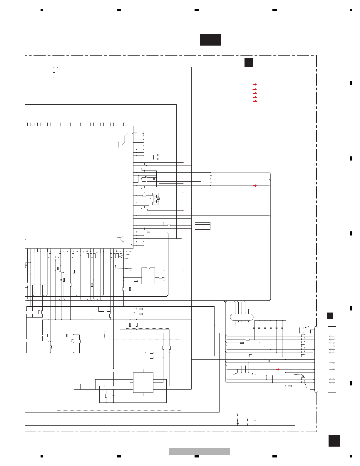
5 678
56
7
8
C
D
F
A
B
E
C
C-b
BSCK
BRST
RESET
BDATA
BRXEN
BSRQ
ROUT
ROUT
LOUT
CONT
LOEJ
BSRQ
BRXEN
BDATA
BSCK
CLCONT
RESET
FLMD0
VDSENS
HOME
8EJ
DP
RESET
RX
TX
FLMD0
USBGND
USBGND
DSCSNS
BRST
TX
RX
VD
VD
PGND PGND
GND
GND
GND
GND
GND
GND
AGND
AGND
DP
DM
SWVDD
VDD VDD
VDD
VDD
VDD
LOUT
X201
1
2
3
Q201
TH201
C203
C208
NM
R258
NM
C201
(1608)
NM
C202
0.1u
C204
0.01u
C206
0.1u
C207
(1608)
0.1u
C211
0.1u
C212
(1608)
NM
C213
0.1u
C214
0.1u
C260
0.1u
R201
(1608)
NM
R202
47k
R203
(1608)
R204
220
R235
47k
R243
(1608)
NM
R254
100k
R256
100k
R2590R261
100k
R702
220
C230
(1608)
NM
C601
NM
C602
NM
C701
NM
C702
NM
C705
NM
C706
(1608)
NM
C707
NM
C730
(1608)
NM
R207
0
R208
NM
R245
NM
R714
(1608)
0
C205
(2125)
4.7u
C209
22u
C210
0.1u
C243
(2125)
NM
C290
0.1u
C294
0.1u
C704
1000p
R206
100k
R209
NM
R210
1k
R223
47k
R233
10k
R234
47k
R244
47k
R249
NM
R250
100
R252
100
R273
10k
R277
10k
R280
10k
R290
10k
R292
2.7k
R293
4.7k
R701
220
DP
AGND1
DM
BSCK
BDATA
BRXEN
BSRQ
ROUT
RESET
BRST
CD3VON
RX
LRCKOK
TX
CDMUTE
LOUT
SCL
BSCK2
SDA
FLMD0
TESTIN
TEMP
ROM
CN704
1
2
345
6
7
8
9
10
RFOK
MIRR
LOCK
HOLD
GND4 GND1GND3
USBGND
VDD
VD_1
VD_2
PGND1PGND2
VDD_2
IC202
CS
1
SK
2
DI
3
DO
45
GND
6
TEST
7
NC
8
VCC
IC205
1
2
3
4
5
6
7
8
9
10
11 12 13
14
15
16
17
18
19
20
C703
100p
CN701
1
VD 7.5V
2
VD 7.5V
3
/BSRQ
4
/BRST
5
/BSCK
6
BRXEN
7
BDATA
8
/RESET
9
VDD 3.3V
10
GND GND
11
ROUT
12
AGND GND
13
LOUT
14
GND GND
15
PGND GND
16
DP
17
DM
18
USBGND GND
19
USBGND GND
C215
0.1u
R28324R282
24
DOUT
SCKO
LRCK
R295
47k
AGND2
IC201
DP5VDDQ6/8SNS7/12SNS8/HOME9DSCSNS
10
VDSENS11TEMP12ADC.VDD
13
ADC.GND
14
FLMD015/RESET16/ADENA
17
CPSEL(/EJSW)18/TESTIN
19
CLCONT20BSI21BSO
22
/BSCK23FTxD24FRxD25BRXEN
26
/BSRQ27LOEJ
28
ROM29CPRDY30/CPRST31SDA
32
SCL
33
ROMDATA34ROMCK
35
ROMCS
36
CDMUTE(MCKRQ)
37
LRCKOK
38
/PUEN
39
CD3VON
40
CONT
41
F_REGC
42
OCI
43
PPON
44
TEST
45
/BRST
46
REGS
47
C.VDD
48
C.GND
49
XTAL
50
X.GND
51
/XTAL
52
X.VDD
53
DA.VDD1
54
LOUT
55
DA.GND1
56
REGC
57
DA.GND2
58
ROUT
59
DA.VDD2
60
D.GND
61
D.VDD
62
REG16
63
LRCK
64
SCKO
65
DOUT
66
SVMON0
67
SVMON1
68
SVMON2
69
SVMON3
70
C33M
71
(/RCS)
72
(CKE)
73
/RAS
74
/CAS0(LDQM)
75
/CAS1(UDQM)
76
/WE
77
/OE(/CAS)
78
RDB079RDB180RDB2
81
RDB3
82
RDB483RDB5
84
RDB6
85
RDB7
86
RDB887RDB9
88
RDB10
89
RDB1190RDB12
91
RDB13
92
RDB1493RDB15
94
IO.GND
95
IO.VDD
96
RA0
97
RA1
98
RA2
99
RA3
100
RA4
101
RA5
102
RA6
103
RA7
104
CPRDY
CPRST
OCI
PUEN
DP2 DM2
R237
470
SWVDD
I/O
343536
72
71
MASK/FLASH
C243
MASK
FLASH
PE5715A
NM
(uPD63790CGJ)
NC1
MODE1/SPI_nSS
NC2
nRESET
VCC
NC3
NC4
NC5
NC6
NC7
VSS
I2C_SCL/SPI_SIMO
I2C_SDA/SPI_SOMI
MODE0/SPI_CLK
NC8
NC9
NC10
NC11
NC12
NC13
NM
NM
NM
NM
2SA1577(QR)
341S2162
iPod CONNECTED MODEL ONLY
NM
CSS1603
16.934 MHz
NM
4.7u
MSC MODEL ONLY
CKS5854
C
CD CORE UNIT (S11USB)
A
CN651
6
i
j
h
g
m
l
k
b
F
SIGNAL LINE
FOCUS SERVO LINE
TRACKING SERVO LINE
CARRIAGE SERVO LINE
SPINDLE SERVO LINE
T
C
S
DEH-22UB/XSUC
49

1234
1234
C
D
F
A
B
E
C-a C-b
C-b
ROUT
LOUT
CONT
BRST
GND
AGND
VDD
X201
1
2
3
C208
NM
C206
0.1u
C207
(1608)
0.1u
C211
0.1u
C212
(1608)
NM
C213
0.1u
C214
0.1u
C230
(1608)
NM
C601NMC602
NM
C205
(2125)
4.7u
C209
22u
C210
0.1u
C243
(2125)
NM
R210
1k
R223
47k
CD3VON
LRCKOK
CDMUTE
RFOK
MIRR
LOCK
HOLD
C215
0.1u
DOUT
SCKO
LRCK
IC201
DP
VDDQ
6
/8SNS
7
/12SNS
8
/HOME
9
DSCSNS
10
VDSENS
11
TEMP
12
ADC.VDD
13
ADC.GND
14
FLMD0
15
/RESET
16
/ADENA
17
CPSEL(/EJSW)
18
/TESTIN
19
CLCONT
20
BSI
21
BSO
22
/BSCK
23
FTxD
24
FRxD
25
BRXEN
26
/BSRQ
27
LOEJ
28
ROM
29
CPRDY
30
/CPRST
31
SDA
32
SCL
33
ROMDATA
34
ROMCK
35
ROMCS
36
CDMUTE(MCKRQ)
37
LRCKOK
38
/PUEN
39
CD3VON
40
CONT
41
F_REGC
42
OCI
43
PPON44TEST
45
/BRST
46
REGS
47
C.VDD
48
C.GND
49
XTAL
50
X.GND
51
/XTAL52X.VDD
53
DA.VDD1
54
LOUT
55
DA.GND1
56
REGC
57
DA.GND2
58
ROUT
59
DA.VDD2
60
D.GND
61
D.VDD
62
REG16
63
LRCK64SCKO65DOUT
66
SVMON0
67
SVMON1
68
SVMON2
69
SVMON3
70
C33M
71
(/RCS)
72
(CKE)
73
/RAS
74
/CAS0(LDQM)
75
/CAS1(UDQM)
76
/WE
77
/OE(/CAS)
78
RDB0
79
RDB1
80
RDB2
81
RDB3
82
RDB4
83
RDB5
84
RDB6
85
RDB7
86
RDB8
87
RDB9
88
RDB10
89
RDB11
90
RDB12
91
RDB13
92
RDB14
93
RDB15
94
IO.GND
95
IO.VDD
96
RA0
97
RA1
98
RA2
99
RA3
100
RA4
101
RA5
102
RA6
103
RA7
OCI
PUEN
R237
470
34
35
36
72
71
MASK/FLASH
C243
MASK
FLASH
PE5715A
(uPD63790CGJ)
CSS1603
16.934 MHz
NM
4.7u
C
CD CORE UNIT (S11USB)
l
b
F
SIGNAL LINE
FOCUS SERVO LINE
TRACKING SERVO LINE
CARRIAGE SERVO LINE
SPINDLE SERVO LINE
T
C
S
50
DEH-22UB/XSUC

5 678
56
7
8
C
D
F
A
B
E
C-a C-b
C-b
BSCK
BRST
RESET
BDATA
BRXEN
BSRQ
ROUT
CONT
LOEJ
BSRQ
BRXEN
BDATA
BSCK
CLCONT
RESET
FLMD0
VDSENS
HOME
8EJ
RESET
RX
TX
FLMD0
USBGND
DSCSNS
TX
RX
VD
GND
GND
GND
GND
AGND
DP
DM
SWVDD
VDD VDD
VDD
VDD
LOUT
Q201
TH201
C203
NM
C201
(1608)
NM
C202
0.1u
C204
0.01u
R201
(1608)
NM
R202
47k
R203
(1608)
R204
220
R235
47k
R243
(1608)
NM
R254
100k
R256
100k
R261
100k
R702
220
C701
NM
C702
NM
C705
NM
C706
(1608)
NM
C707
NM
C730
(1608)
NM
R207
0
R208
NM
R245
NM
R714
(1608)
0
C243
(2125)
NM
C290
0.1u
C294
0.1u
C704
1000p
R206
100k
R209
NM
R210
1k
47k
R233
10k
R234
47k
R244
47k
R249
NM
R250
100
R252
100
R273
10k
R277
10k
R280
10k
R290
10k
R292
2.7k
R293
4.7k
R701
220
DP
AGND1
DM
BSCK
BDATA
BRXEN
BSRQ
ROUT
RESET
BRST
CD3VON
RX
LRCKOKTXCDMUTE
LOUT
SCL
BSCK2
SDA
FLMD0
TESTIN
TEMP
ROM
CN704
1
2
3
4
5
6
7
8
9
10
GND4 GND1GND3
USBGND
VDD
VD_1
VD_2
PGND1PGND2
VDD_2
IC202
CS1SK2DI3DO
45
GND
6
TEST
7NC8
VCC
IC205
1
2
3
4
5
6
7
8
9
10
11 12 13
14
15
16
17
18
19
20
C703
100p
CN701
1
VD 7.5V2VD 7.5V3/BSRQ4/BRST5/BSCK6BRXEN7BDATA8/RESET9VDD 3.3V10GND GND11ROUT12AGND GND13LOUT14GND GND15PGND GND16DP17DM18USBGND GND19USBGND GND
R283
24
R295
47k
AGND2
DP
VDDQ
6
/8SNS
7
/12SNS
8
/HOME
9
DSCSNS
10
VDSENS
11
TEMP
12
ADC.VDD
13
ADC.GND
14
FLMD0
15
/RESET
16
/ADENA
17
CPSEL(/EJSW)
18
/TESTIN
19
CLCONT
20
BSI
21
BSO
22
/BSCK
23
FTxD
24
FRxD
25
BRXEN
26
/BSRQ
27
LOEJ
28
ROM
29
CPRDY
30
/CPRST
31
SDA
32
SCL
33
ROMDATA
34
ROMCK
35
ROMCS
36
CDMUTE(MCKRQ)
37
LRCKOK
38
/PUEN
39
CD3VON
40
CONT
41
F_REGC
42
OCI
43
CPRDY
CPRST
PUEN
DP2 DM2
SWVDD
I/O
34
35
36
MASK
FLASH
NM
NC1
MODE1/SPI_nSS
NC2
nRESET
VCC
NC3
NC4
NC5
NC6
NC7
VSS
I2C_SCL/SPI_SIMO
I2C_SDA/SPI_SOMI
MODE0/SPI_CLK
NC8
NC9
NC10
NC11
NC12
NC13
NM
NM
NM
NM
2SA1577(QR)
341S2162
iPod CONNECTED MODEL ONLY
NM
NM
4.7u
MSC MODEL ONLY
CKS5854
A
CN651
6
i
j
h
g
m
l
k
DEH-22UB/XSUC
51

1234
1234
C
D
F
A
B
E
C-bC-a
C-a
C-b
1
TOP2FOP3FOM4TOM
5MD6
A+C
7VR8
VREF
9
P1+P6
10
GND
11
P5+P10
12
VCC13B+D14LD+15LD-
FOCUS ACT
TRK ACT
P4
LD
VCC
P8
P2P1P6
P5
P10
P3P9P7
MD
HOLOGRAM UNIT
E:P5+P10
F:P1+P6
M1 CXE2273
SPINDLE MOTOR
PD
EFBD
AC
MD
SDFDTD
BD
E
F
AC
TOM
FOM
FOP
TOP
PD
REFOUT
REFOUT
SOM
GND
GND
VDDVDD
Q101
C102
NM
C213
C216
3300p
C217
0.1u
C218
0.047u
C219
0.1u
C220
1800p
C221
0.1u
C224
0.1u
C226
68p
C227
47p
C236
0.1u
C240
0.1u
C250
1000p
C251
1000p
R221
10k
R222
10k
R225
10k
R226
39k
C105 C110
C111
NM
R106
NM
R108
NM
R236
NM
C106
(2125)
4.7u
C222
56p
C223
4p
C228
0.01u
C229
0.1u
C239
22p
C293
1000p
R101
2.4
R102
2.4
R103
2.7
R104
2.2k
R107
1MEG
R214
4.7k
R216
4.7k
R227
5.6k
R228
1.2k
R229
4.7k
R232
1.2k
R291
2.7k
ADIN
TE
TEC
FE
RFO
ATEST
LD
F
B+D
PD
E
A+C
RFAGC
D101
BLK
REFO1
PU+3V
LD1
V3R3
CN101
123456789
10
1112131415
Q102
USBXTAL
1
/USBXTAL
2
GNDQ
3
DM
4
DP
5
VDDQ
6
/8SNS
7
/12SNS
8
/HOME
9
DSCSNS
10
VDSENS
11
TEMP
12
13
96
RA0
97
RA1
98
RA2
99
RA3
100
RA4
101
RA5
102
RA6
103
RA7
104
RA8
105
RA9
106
RA10
107
RA11
108
FD
109TD110SD111MD112
EFM
113
ASY
114
ATEST
115
A.VDD1
116
A.GND1
117
RFI
118
AGCO
119
C3T
120
AGCI
121
RFO
122
EQ2
123
EQ1
124
RF2-
125
RF-
126
A.GND2
127
A.VDD2
128A129B130F131E132
REFOUT
133
FE-
134
FEO
135
ADCIN
136
TE-
137
TEO
138
TE2
139
TEC
140LD141PD142
AD.VDD
143
AD.GND
144
(1/10SR,1608)
(1/10W)
CXX1942
F.ACT:Applying positive voltage to FOP.
the lens moves DISC side.
T.ACT:Applying positive voltage to TOP.
the lens moves outer circumference.
1
2
(12)
(13)
PICKUP UNIT (P10.5)(SERVICE)
NOTE1) GND.... CD LSI, RFAMP, CPU
PGND...Actuator, Motor Driver
AGND...Audio
These GND's are not connected to each other on PCB.
PGND is connected to a floating mechanism part by a screw.
NM
UNR511MG
2SA1577
NM NM
CKS4808
f
c
d
F
T
F
T
T
T
F
F
T
F
F
T
S
F
C
S
T
52
DEH-22UB/XSUC
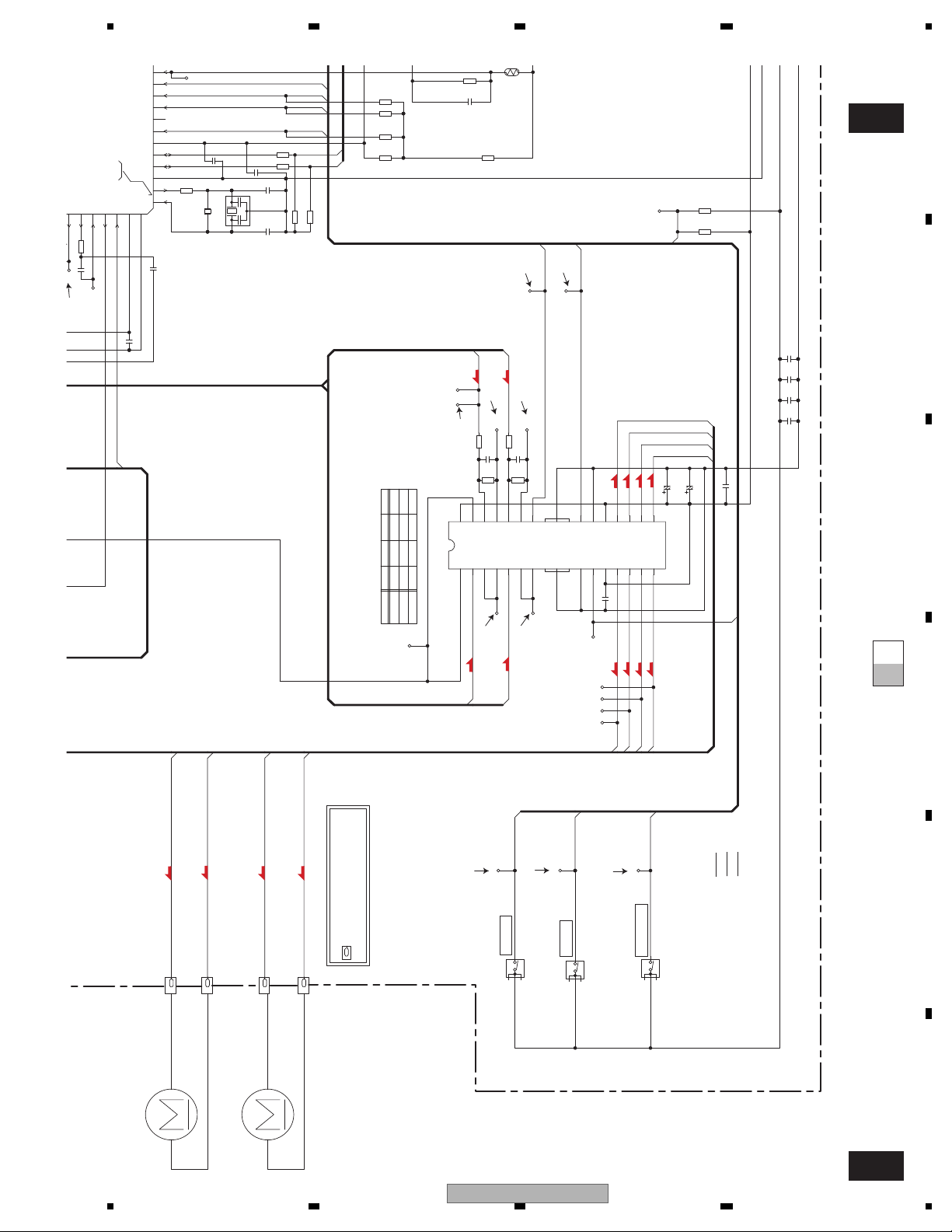
5 678
56
7
8
C
D
F
A
B
E
C-a
C-b
C-bC-a
M2 CXC4026
LOADING/CARRIAGE
MOTOR
M1 CXE2273
SPINDLE MOTOR
VDSENS
HOME
8EJ
DM
DP
PD
REFOUT
TD
FD
CONT
FOP
FOM
TOM
TOP
SOM
SOP
LCOM
LCOP
LOEJ
CLCONT
SD
DSCSNS
8EJ
SOM
SOP
LCOM
LCOP
MD
USBGND
HOME
DSCSNS
VDSENS
VD
VD
VD
VD
PGND
PGND
PGND
GNDGND
X205
IC301
VR1OPIN2+2OPIN2-3OPOUT2
4
5
OPIN1+6OPIN1-7OPOUT129FIN19MUTE10PowVcc111VO1-12VO1+13VO2-14VO2+
8
GND1
15
VO3+
17
VO4+
18
VO4-
19
PowVcc2
20
GND2
21
CNT
22
LDIN
23
OPOUTSL
24
OPINSL
25
OPOUT3
26
OPIN3-
27
OPIN3+
28
PreVcc
16
VO3-
30
FIN2
TH201
C203
C263
NM
C708
NM
R258
NM
C202
01u
C240
0.1u
C260
0.1u
C303
4700p
C304
0.022u
C711
0.1u
R203
(1608)
R254
100k
R256
100k
R259
0
R261
100k
R307
18k
R308
18k
R310
18k
R309
18k
C305
NM
C709
NM
C710
NM
C228
0.01u
C293
1000p
C308
(1608)
NM
R240
(1608)
47k
R241
10k
R284
15k
R285
15k
R291
2.7k
TE
TEC
TEMP
CLCONT
VDSENS
MDX
LOEJ
TIN
CONT
HOME
8SNS
TOM
DSCSNS
FOM
FOP
SIN
TOP
FIN
CIN
MDY
RED
OG
PL
BLK
REFO2
X203
1
2
3
S905
1
NC
2
34
NC
S901
1
NC
2
3
4
NC
C306
NM
R294
220
S903
1
NC
2
3
4
NC
C307
(1608)
1u
R283
24
R282
24
USBXTAL
1
/USBXTAL
2
GNDQ
3
DM
4
DP
5
VDDQ
6
/8SNS
7
/12SNS
8
/HOME
9
DSCSNS
10
VDSENS
11
TEMP
12
13
TEO
138
TE2
139
TEC
140LD141PD142
AD.VDD
143
AD.GND
144
C261
3p
C262
3p
MOTOR DRIVER LOGIC TABLE
LOAD
CLCONT H H L L
LOEJ L H - -
CONT L L H L
Land for manual soldering
1
2
HOME
8SNS
DSCSNS
CSN1067-A
CSN1068-A
CSN1068-A
BA5839FP
EJ
PLAY
OFF
CSS1753
48.000 MHz
NM
NM
NM
SWITCHES:
CD CORE UNIT
S901:HOME SWITCH.........ON-OFF
S903:DSCSNS SWITCH.....ON-OFF
S905:8EJ SWITCH..............ON-OFF
The underlined indicates the switch position.
1
2
3
9
a
7
8
4
5
d
e
T
F
F
T
S
S
C
C
S
S
C
C
F
T
S
C
DEH-22UB/XSUC
53

1234
1234
C
D
F
A
B
E
10.4 WAVEFORMS
- CD CORE UNIT Note : 1. The encircled numbers denote measuring points in the circuit diagram.
2. Reference voltage REFO1(1.65 V)
500 ms/div5 V/div
5 V/div
5 V/div
10 V/div
DSCSNS
CLCONT
LOEJ
VD
5 V/div
5 V/div
5 V/div
5 V/div
DSCSNS
8SNS
12SNS
LOEJ
5 V/div
5 V/div
5 V/div
5 V/div
500 ms/divDSCSNS
8SNS
12SNS
LOEJ
500 mV/div
500 mV/div
200 ms/divTE
FE
200 mV/div
2 V/div
2 V/div
500 ms/divFIN
RFOK(MONI_2)
SIN
1 V/div
500 mV/div
1 V/div
1 s/div
500 ms/div
SIN
CIN
TIN
2 V/div
500 mV/div
5 us/divMDX
SIN
2 V/div
500 mV/div
200 ms/divMDX
SIN
500 mV/div
500 mV/div
500 mV/div
500 mV/div
20 ms/divFE
FIN
TE
TIN
1 V/div
500 mV/div
500 mV/div
500 us/divRFAGC
TE
TIN
500 mV/div
500 mV/div
2 ms/div TE
RFAGC
500 mV/div
500 mV/div
200 ms/divFIN
FE
Source On setup operation12 cm CD-DA Source On setup operation
CD-DA Play operation Spindle waveform during play operation Spindle waveform during play operation
(Wider)
Focus Search waveform Track Open waveform 1 Track Jump waveform
12 cm CD-DA setup operation after loading
12 cm CD Loading operation 12 cm CD Loading operation 8 cm CD Loading operation
Ref.:
GND
Mode:
Normal
Ref.:
GND
Mode:
Normal
Ref.:
GND
Mode:
Normal
Ref.:
REFO
Mode:
Normal
Ref.:
REFO
Mode:
Normal
Ref.:
REFO
Mode:
Normal
Ref.:
REFO
Mode:
TEST
Ref.:
REFO
Mode:
TEST
Ref.:
REFO
Mode:
TEST
Ref.:
REFO
Mode:
Normal
Ref.:
REFO
Mode:
Normal
Ref.:
REFO
Mode:
Normal
54
DEH-22UB/XSUC

5 678
56
7
8
C
D
F
A
B
E
1 V/div
500 mV/div
500 mV/div
2 ms/divRFAGC
TE
TIN
1 V/div
500 mV/div
500 mV/div
500 us/divRFAGC
TE
TIN
1 V/div
500 mV/div
500 mV/div
500 us/divRFAGC
TE
TIN
5 V/div
5 V/div
5 V/div
5 V/div
500 ms/divDSCSNS
8SNS
HOME
LOEJ
1 V/div
1 V/div
200 us/divLOUT
ROUT
1 V/div
1 V/div
1 V/div
2 V/div
200 ms/divRFAGC
TE
CIN
SIN
1 V/div
1 V/div
1 V/div
1 V/div
500 us/divRFAGC
TIN
TE
FIN
5 V/div
5 V/div
5 V/div
5 V/div
500 ms/divDSCSNS
8SNS
HOME
LOEJ
5 V/div
5 V/div
5 V/div
500 ms/divDSCSNS
CLCONT
LOEJ
12 cm CD Eject operationAnalog audio waveform
12 cm CD Eject operation 8 cm CD Eject operation Black dot(800 um) during play
Search operation(Outter to Inner)
4 Tracks Jump waveform 10 Tracks Jump waveform 32 Tracks Jump waveform
Ref.:
REFO
Mode:
TEST
Ref.:
REFO
Mode:
TEST
Ref.:
REFO
Mode:
TEST
Ref.:
GND
Mode:
Normal
Ref.:
REFO
1 V/div
1 V/div
50 ms/divDP
DM
2 V/div
2 V/div
50 ms/divDP
DM
1 V/div
1 V/div
50 ns/divDP
DM
USB Play USB device inserting to USB connector. CD Play with USB(iPod) device connecting.
Ref.:
USB
GND
Ref.:
USB
GND
Ref.:
USB
GND
Mode:
Normal
Ref.:
GND
Mode:
Normal
Ref.:
REFO
Mode:
Normal
Ref.:
GND
Mode:
Normal
Ref.:
AGND
Mode:
Normal
DEH-22UB/XSUC
55

1234
1234
C
D
F
A
B
E
2 V/div
2 V/div
2 V/div
500 ms/divCPRST
SDA
SCL
2 V/div
2 V/div
50 ms/divDP
DM
ACC OFF with USB(iPod) device connecting. iPod Authentication Operation
Ref.:
USB
GND
Ref.:
GND
56
DEH-22UB/XSUC

5 678
56
7
8
C
D
F
A
B
E
DEH-22UB/XSUC
57

1234
1234
C
D
F
A
B
E
11. PCB CONNECTION DIAGRAM
A
A
TUNER AMP UNIT
Capacitor
Connector
P.C.Board
Chip Part
SIDE B
SIDE A
NOTE FOR PCB DIAGRAMS
1.The parts mounted on this PCB
include all necessary parts for
several destination.
For further information for
respective destinations, be sure
to check with the schematic dia gram.
2.Viewpoint of PCB diagrams
10 20 30 40 50 60
X
150
140
130
120
110
100
90
80
70
60
50
40
30
20
10
0
Y
51
1
1
1
1
1
1
5
1
1
1
R251
R252
R253
R254
R255
R256
R257
R258
CN251
C251
C252
C253
C254
C255
C256
C257
C258
C259
Q301
L501
Q351
R301
R302
R303
R501
R502
R503
R504
R505
R506
R507
C501
C502
C503
C504
C505
C506
C313
R351
R352
R353
C711
R941
C712
R942
C335
C336
C337
CN941
FU251
C351
C941
C942
D501
D502
IC501
Q251
Q252
IC712
W.REM
RCA
11.1 TUNER AMP UNIT
58
DEH-22UB/XSUC

5 678
56
7
8
C
D
F
A
B
E
A
SIDE A
160
E
1
5
1 5
10
1 5
10
15
20
1
515
0201
1
1 5
10
15
1
1 5
10
15
20
1
1
E
E
1
1510
15
20
15
51
10
1
5
E
E
E
E
E
1 5
10
15
20
25
1
0151
R401
R404
R405
D751
R406
R407
R213
R408
R409
Q851
R601
R602
R603
R604
R410
R605
R411
D951
R412
R606
D952
R413
R607
R608
R609
R221
R222
R801
R802
R803
R804
R610
R805
R611
L851
R612
R806
CN402
R613
R807
R808
R615
R809
R616
R617
R618
R619
R810
R811
R812
CN602
R813
R814
Q680
R620
R815
R816
R622
R817
R623
R818
R819
C201
IC951
C202
C203
C204
C205
C206
C207
R820
C401
C402
C403
C404
C405
C406
C212
C407
C213
C408
C214
C409
C215
C216
R831
C601
R832
C602
C603
C410
C411
C605
C606
C412
R836
R643
C607
R837
C413
C414
C608
C609
C415
C416
C417
C801
C802
C803
C610
C804
C611
X601
C805
C612
C806
C613
C807
C614
C808
C615
C809
C616
C617
C618
R655
C619
R656
R657
C810
R659
CN831
C811
CN832
C812
C813
C620
C814
C621
C815
R851
C816
C622
R852
C817
C623
R853
C818
R660
C624
R854
C819
R661
C625
R855
R662
C626
R663
C627
R664
C628
R665
C629
R666
C820
C821
C822
C630
CN651
C631
S801
C632
C633
C635
R672
C636
C637
R674
C638
R675
C639
R676
R677
R678
R679
C257
C640
C641
C642
R680
C645
R681
C647
R683
R685
R686
R687
R688
Q301
R689
C650
C651
C653
R691
R692
D601
D602
IC201
D801
D802
D804
D805
C671
D806
C672
D807
L701
L702
IC601
C681
C682
C683
L902
L903
X681
Q921
R301
R302
R303
Q751
Q752
D851
Z401
R701
R702
R703
R704
R708
R712
R331
R332R333
R334
R916
C301
C302
C303
C304
C305
C306
C307
C308
C309
R921
JA901
R922
R923
R924
R925
C310
C311
C312
C313
R351
R352
R353
C702
C703
C704
AR401
C901
IC691
R751
C909
C331
C332
C333
C334
C910
C911
C335
C912
C336
C913
C337
C914
C915
R951
C916
C917
C918
C919
C920
C921
D301
D302
C751
C752
L201
Q601
C951
C952
C953
L401
L402
L403
Q801
Q802
Q803
Q804
IC301
D901
L601
D902
L602
L603
L604
L605
ANT401
L606
L607
L608
L609
L801
L802
L610
D911
L611
D912
L612
L613
L614
L615
L616
L617
L618
L619
L620
D921
L621
IC911
R201
R206
R207
D803
1
10
20
30
40
50
60
70
80
90
100
110120
130
140
FRONT
FM/AM TUNER UNIT
ANTENNA
B
CN1821
C
CN701
CORD ASSY
FU 251 (A,5,129) Fuse 3 A CEK1286
>
DEH-22UB/XSUC
59

1234
1234
C
D
F
A
B
E
A
A
TUNER AMP UNIT
160 150 140 130 120 110 100 90 80
1
1
1
1
60
DEH-22UB/XSUC

5 678
56
7
8
C
D
F
A
B
E
A
SIDE B
080706050403020
X
150
140
130
120
110
100
90
80
70
60
50
40
30
20
10
0
Y
10
1
1
DEH-22UB/XSUC
61

1234
1234
C
D
F
A
B
E
11.2 KEYBOARD UNIT
KEYBOARD UNIT
B
D1870
D1889
S1842
S1841
CLOCK
EJECT
D1869
D1888
D1851
1 5 10 15 20 25 30 35 40
AUX
CN1901
1
5
USB
CN1911
1
1
IC1802
LCD1801
160
SIDE A
S1832
D1886
D1867
LIST
S1831
C1855
D1874
D1855
3
S1840
D1875
D1856
2
S1839
1
S1838
PWR/VOL
C1856
D1876
D1857
1
C1859
RIGHT
D1877
D1858
D1878
D1859
S1828
C1858
S1827
D1871
D1852
S1845
C1854
C1853
C1852
6
S1835
D1872
D1853
D1873
5
D1887
D1868
C1868
D1854
5
S1836S1837
4
C1860
D1879
D1860
C1863
S1823
C1866
S1830
D1882
D1863
DOWN
S1829
S1834
D1885
D1866
BAND/ESC
S1833
10
Y
10 20 30 40 50 60 70 80 90 100 110 120 130 140 150
X
0
S1826
D1880
UP
D1861
S1825
S1822
D1883
D1864
SRC
D1884
S1843
S1844
DISP/BACK
B
62
S1821
D1865
40
DEH-22UB/XSUC
30
C1861
C1864
C1862
S1824
D1881
D1862
LEFT
C1865
20

5 678
56
7
8
C
D
F
A
B
E
B
SIDE B
B
KEYBOARD UNIT
160 150 140 130 120 110 100 90 80 70 60 50 40 30 20
X
40
30
20
10
0
Y
10
1
5
151
2010
1 5 10 15
20 25 30
35 40 45
50 55 60
5
1
1
X1801
C1901
C1902
C1903
C1904
C1905
R1901
R1902
D1911
D1912
R1911
R1912
C1801
C1802
CN1821
D1801
D1802
R1801
R1802
R1803
R1804
R1805
R1806
IC1801
R1821
R1822
R1823
R1824
R1825
R1826
C1851
Q1851
C1857
L1911
C1867
C1869
C1870
R1851
R1852R1853
R1854
R1855
R1856
R1857
R1858
R1859R1860
R1861
R1862
R1863
R1864
R1865
R1866
R1867
R1868
R1869
R1870
R1871
R1872
R1873
R1874
R1875
R1876
R1877
R1878
VA1901
VA1902
VA1903
VA1904
A
CN832
DEH-22UB/XSUC
63

1234
1234
C
D
F
A
B
E
11.3 CD CORE UNIT(S11USB)
CD CORE UNIT(S11USB)
C
SIDE A
PICKUP UNIT(P10.5)(SERVICE)
60
TH201
40
R203
R701
C203
4550
C206
C213
1
C207
1
X201
55606570
S901
HOME
80859095100105
C214
C211
C208
R237
LOADING/CARRIAGE
M2
MOTOR
M1
SPINDLE
MOTOR
R310
C708
C304
R309
R308
C303
R307
IC301
15
2025
30
29
0151
C307
75
C711
C201
R202
1
IC202
R243
R201
5
R234
CN101
1 5 10 15
C250
50
C102
D101
CN704
1 5
10
40
30
R294
R261
R259
20
15
X203
1
R282
R283
R258
IC205
C240
10
F
E
C226
C227
C263
R256
20
REFO1
C220
C219
C221
C224
135140
15 101520253035
C260
C202
R254
R702
C204
C290
R204
1 5
C216
C218
R226
C217
R225
110115120125130
R221
IC201
C251
R222
10
CN701
Y
1 5 10 15
0
10 20 30 40 50 60 70
A
CN651
X
C
64
DEH-22UB/XSUC

5 678
56
7
8
C
D
F
A
B
E
C
SIDE B
C
CD CORE UNIT(S11USB)
70 60 50 40 30 20 10
X
60
50
40
30
20
10
0
Y
1
E
E
1
1
E
R210
R214
R216
R223
R227
R228
R229
R232
R233
R235
R236
R240
R241
C205
R244
R245
C209
R249
C210
C212
R250
X205
C215
R252
C601
C602
C222
C223
C228
C229
C230
C236
R273
C239
R277
C243
R280
R284
R285
R290
R291
R292
R293
Q101
R295
Q102
C261
C262
C293
C294
R101
R102
R103
R104
R106
R107
R108
R714
C105
C106
C110
C111
C305
C306
C308
C701
C702
C703
C704
C705
C706
C707
C709
C710
C730
S903
S905
Q201
R206
R207
R208
R209
8EJ
DSCSNS
DEH-22UB/XSUC
65

1234
1234
C
D
F
A
B
E
12. ELECTRICAL PARTS LIST
NOTE:
Parts whose parts numbers are omitted are subject to being not supplied.
The part numbers shown below indicate chip components.
Chip Resistor
RS1/_S___J,RS1/__S___J
Chip Capacitor (except for CQS.....)
CKS....., CCS....., CSZS.....
The > mark found on some component parts indicates the importance of the safety factor of the part.
Therefore, when replacing, be sure to use parts of identical designation.
Meaning of the figures and others in the parentheses in the parts list.
Example) IC 301 is on the point (face A, 91 of x-axis, and 111 of y-axis) of the corresponding
PC board.
IC 301 (A, 91, 111) IC NJM2068V
Circuit Symbol and No. Part No.
Unit Number: YWM5449
Unit Name : Tuner Amp Unit
Unit Number :
Unit Name : Keyboard Unit
Unit Number: CWX3776
Unit Name : CD Core Unit(S11USB)
A
Unit Number: YWM5449
Unit Name : Tuner Amp Unit
MISCELLANEOUS
IC 201 (A,102,109) IC PML014A
IC 301 (A,74,141) IC PAL007C
IC 501 (A,16,114) IC BD9007F
IC 601 (A,117,83) IC PN5035B
IC 712 (A,36,123) IC BD6538G
IC 911 (A,141,28) IC BA49181-V12
Q 251 (A,21,130) Transistor UMH3N
Q 351 (A,31,131) Transistor RT3T22M
Q 601 (A,136,63) Transistor 2SD1858
Q 751 (A,137,139) Transistor 2SD2396
Q 752 (A,136,128) Transistor RT3T22M
Q 801 (A,107,42) Transistor 2SA1036K
Q 802 (A,107,38) Transistor RT1N141M-11
Q 921 (A,127,106) Transistor LSC4081UB
D 301 (A,93,128) Diode 1SR154-400
D 302 (A,113,114) Diode 1SR154-400
D 501 (A,17,125) Diode 1SR154-400
D 502 (A,23,107) Diode RB160L-40
D 751 (A,135,132) Diode HZU7R5(B3)
D 801 (A,108,22) Diode MALS068X
D 802 (A,108,21) Diode MALS068X
D 803 (A,114,21) Varistor EZJP0V270RM
D 804 (A,115,22) Varistor EZJP0V270RM
D 901 (A,133,123) Diode 1SR154-400
Circuit Symbol and No. Part No.
D 902 (A,127,117) Diode 1SR154-400
D 911 (A,113,56) Diode 1SR154-400
D 912 (A,113,53) Diode 1SR154-400
D 921 (A,123,106) Diode HZU6R2(B3)
L 402 (A,146,97) Inductor LCTAW2R2J2520
L 403 (A,146,57) Inductor CTF1473
L 501 (A,29,110) Choke Coil 47 uHCTH1420
L 602 (A,121,98) Inductor CTF1473
L 606 (A,136,85) Chip Coil LCTAW1R0J2520
L 607 (A,133,83) Inductor CTF1379
L 608 (A,133,72) Chip Coil LCTAW1R5J2520
L 609 (A,134,70) Chip Coil LCTAW1R5J2520
L 610 (A,136,77) Inductor LCTAW1R2J2520
L 611 (A,138,71) Inductor CTF1379
L 612 (A,137,69) Inductor CTF1379
L 614 (A,122,69) Inductor CTF1379
L 617 (A,132,85) Inductor CTF1389
L 618 (A,121,65) Inductor CTF1389
L 701 (A,93,47) Inductor CTF1713
L 702 (A,93,48) Inductor CTF1473
L 801 (A,94,31) Inductor LCTAW2R2J2520
L 902 (A,107,140) Choke Coil 600 uHCTH1432
X 601 (A,141,78) Oscillator 74.1 MHzCSS1758
X 681 (A,114,62) Oscillator 4.7186 MHzCSS1796
FU251 (A,5,129) Fuse 3 A CEK1286
AR401 (A,145,110) Surge ProtectorIMSA-6802-01Y900
ANT401 (A,153,128) Antenna Jack CKX1070
CN251 (A,17,139) Pin Jack YKB5010
CN651 (A,85,40) Connector CKS3833
CN832 (A,105,3) Connector CKS6188
JA901 (A,109,141) Plug CKM1586
Z 401 (A,153,105) FM/AM Tuner UnitCWE2025
RESISTORS
R 201 (A,118,97) RAB4CQ102J
R 206 (A,90,112) RS1/16SS681J
R 207 (A,91,105) RS1/16SS681J
R 213 (A,90,107) RS1/16SS331J
R 221 (A,91,106) RS1/16SS223J
R 222 (A,91,112) RS1/16SS223J
66
DEH-22UB/XSUC

5 678
56
7
8
C
D
F
A
B
E
Circuit Symbol and No. Part No.
R 251 (A,19,131) RS1/16SS223J
R 252 (A,24,131) RS1/16SS223J
R 253 (A,27,131) RS1/16SS821J
R 254 (A,17,131) RS1/16SS821J
R 303 (A,59,132) RS1/16SS153J
R 331 (A,71,126) RS1/16SS471J
R 332 (A,79,128) RS1/16SS471J
R 333 (A,71,128) RS1/16SS471J
R 334 (A,78,126) RS1/16SS471J
Circuit Symbol and No. Part No.
R 680 (A,96,99) RS1/16SS273J
R 681 (A,95,101) RS1/16SS473J
R 683 (A,95,76) RS1/10SR473J
R 685 (A,101,97) RS1/16SS104J
R 686 (A,104,97) RS1/16SS104J
R 687 (A,104,96) RS1/16SS104J
R 689 (A,93,74) RS1/16SS0R0J
R 702 (A,94,40) RS1/16SS221J
R 704 (A,92,37) RS1/16SS221J
R 351 (A,57,127) RS1/16SS103J
R 352 (A,55,130) RS1/16SS153J
R 353 (A,55,129) RS1/16SS221J
R 401 (A,145,55) RS1/16SS0R0J
R 404 (A,129,94) RS1/16SS102J
R 405 (A,147,47) RS1/16SS102J
R 406 (A,136,91) RS1/16SS102J
R 407 (A,136,90) RS1/16SS102J
R 408 (A,140,93) RAB4CQ104J
R 409 (A,131,92) RS1/16SS391J
R 410 (A,131,91) RS1/16SS681J
R 411 (A,133,91) RS1/16SS681J
R 412 (A,131,90) RS1/16SS681J
R 413 (A,131,89) RS1/16SS472J
R 501 (A,11,114) RS1/16SS473J
R 502 (A,11,113) RS1/16SS392J
R 503 (A,22,113) RS1/16SS183J
R 504 (A,18,117) RS1/10SR4702F
R 505 (A,16,117) RS1/16SS682J
R 506 (A,16,120) RS1/10SR1002F
R 507 (A,18,120) RS1/10SR471J
R 601 (A,103,89) RS1/16SS473J
R 602 (A,101,78) RS1/16SS222J
R 603 (A,95,69) RS1/16SS473J
R 604 (A,132,87) RS1/16SS681J
R 708 (A,94,35) RS1/16SS104J
R 712 (A,94,84) RS1/16SS103J
R 751 (A,133,132) RS1/4SA271J
R 802 (A,109,42) RS1/16SS103J
R 803 (A,107,40) RS1/16SS562J
R 804 (A,98,22) RS1/10SR101J
R 805 (A,101,22) RS1/10SR101J
R 810 (A,96,26) RS1/10SR222J
R 811 (A,94,26) RS1/10SR222J
R 812 (A,111,26) RS1/10SR222J
R 813 (A,110,26) RS1/10SR222J
R 814 (A,113,26) RS1/10SR222J
R 815 (A,114,26) RS1/10SR222J
R 816 (A,92,71) RS1/16SS104J
R 817 (A,106,31) RS1/16SS473J
R 818 (A,94,69) RS1/16SS104J
R 819 (A,90,21) RS1/16SS102J
R 820 (A,103,41) RS1/10SR103J
R 831 (A,104,26) RS1/10SR222J
R 832 (A,102,25) RS1/10SR222J
R 836 (A,91,71) RS1/16SS104J
R 837 (A,103,25) RS1/16SS222J
R 855 (A,93,120) RS1/16SS473J
R 921 (A,129,104) RS1/16SS104J
R 922 (A,125,106) RS1/16SS223J
R 606 (A,123,63) RS1/16SS473J
R 607 (A,110,49) RS1/16SS473J
R 608 (A,131,79) RS1/16SS470J
R 610 (A,129,69) RS1/16SS473J
R 611 (A,131,76) RS1/16SS182J
R 612 (A,88,115) RS1/16SS563J
R 613 (A,130,86) RS1/16SS302J
R 615 (A,92,102) RS1/16SS563J
R 616 (A,129,97) RS1/16SS104J
R 617 (A,116,96) RS1/16SS473J
R 618 (A,129,95) RS1/16SS473J
R 619 (A,129,96) RS1/16SS104J
R 622 (A,132,80) RS1/16SS0R0J
R 623 (A,127,70) RS1/16SS0R0J
R 643 (A,128,99) RS1/16SS104J
R 656 (A,101,70) RS1/16SS104J
R 657 (A,98,70) RS1/16SS104J
R 659 (A,103,71) RS1/16SS472J
R 660 (A,100,70) RS1/16SS472J
R 661 (A,103,83) RS1/16SS221J
R 666 (A,136,89) RS1/16SS103J
R 674 (A,102,94) RS1/16SS104J
R 675 (A,93,69) RS1/16SS473J
R 677 (A,99,94) RS1/16SS473J
R 678 (A,89,101) RS1/16SS103J
R 923 (A,117,116) RS1/4SA102J
R 924 (A,120,106) RS1/16SS473J
R 925 (A,121,108) RS1/16SS473J
CAPACITORS
C 201 (A,93,103) CKSSYB224K6R3
C 202 (A,92,115) CKSSYB224K6R3
C 203 (A,93,104) CKSRYB105K6R3
C 204 (A,93,114) CKSRYB105K6R3
C 205 (A,110,105) 10 uF CCG1192
C 206 (A,93,112) CKSRYB105K6R3
C 207 (A,93,106) CKSRYB105K6R3
C 212 (A,93,111) CKSRYB105K6R3
C 213 (A,93,107) CKSRYB105K6R3
C 214 (A,116,105) 4.7 uF CCG1201
C 215 (A,113,106) CKSSYB104K10
C 216 (A,107,102) CCSRCH100D50
C 253 (A,43,130) CEVW2R2M50
C 254 (A,26,127) CEVW2R2M50
C 301 (A,70,129) CKSRYB474K10
C 302 (A,68,129) CKSRYB474K10
C 303 (A,76,128) CKSRYB474K10
C 304 (A,77,128) CKSRYB474K10
C 305 (A,71,132) CKSQYB474K25
C 306 (A,69,132) CKSQYB474K25
R 679 (A,99,100) RS1/16SS103J
DEH-22UB/XSUC
67

1234
1234
C
D
F
A
B
E
Circuit Symbol and No. Part No.
C 307 (A,75,131) CKSQYB474K25
C 308 (A,76,131) CKSQYB474K25
C 309 (A,82,127) CKSQYB225K10
C 310 (A,84,127) CKSQYB225K10
C 311 (A,98,128) CKSRYB104K16
C 312 (A,64,129) CEVW100M16
C 313 (A,53,135) CKSRYB104K16
C 331 (A,69,125) CCSSCH101J50
C 332 (A,79,129) CCSSCH101J50
C 333 (A,71,130) CCSSCH101J50
Circuit Symbol and No. Part No.
C 711 (A,33,122) CKSRYB105K6R3
C 712 (A,39,124) CKSRYB105K6R3
C 751 (A,137,132) CKSSYB473K10
C 752 (A,143,130) CEVW101M16
C 802 (A,99,26) CKSRYB104K16
C 803 (A,102,29) CCSRCH221J50
C 804 (A,98,29) CCSRCH221J50
C 805 (A,94,21) CKSRYB104K16
C 806 (A,94,22) CKSRYB104K16
C 807 (A,103,22) CKSRYB104K16
C 334 (A,76,126) CCSSCH101J50
C 351 (A,47,136) CEVW330M10
C 401 (A,146,58) CCSRCH270J50
C 402 (A,143,96) CKSSYB103K16
C 404 (A,144,104) CEVW101M16
C 405 (A,143,98) CKSSYB103K16
C 409 (A,131,93) CCSSCH100D50
C 416 (A,133,92) CCSSCH390J50
C 501 (A,8,122) CEVW221M16
C 502 (A,9,113) CKSQYB225K16
C 503 (A,21,114) CCSSCH220J50
C 504 (A,23,113) CKSRYB153K50
C 505 (A,26,119) CEVW221M10
C 601 (A,98,88) CKSRYB105K6R3
C 603 (A,102,88) CKSSYB103K16
C 605 (A,111,68) CKSSYB104K10
C 606 (A,103,63) CKSSYB103K16
C 607 (A,117,69) CKSRYB105K6R3
C 609 (A,129,66) CKSRYB331K50
C 610 (A,104,49) CEVW101M4
C 611 (A,129,65) CKSRYB331K50
C 612 (A,119,69) CKSRYB103K50
C 613 (A,99,57) CEVW471M10
C 614 (A,146,92) CKSSYB102K50
C 615 (A,129,68) CKSRYB331K50
C 808 (A,105,22) CKSRYB104K16
C 809 (A,103,21) CKSRYB104K16
C 810 (A,111,21) CCSRCH221J50
C 811 (A,111,22) CCSRCH221J50
C 812 (A,103,38) CKSRYB104K16
C 818 (A,96,22) CKSRYB104K16
C 819 (A,91,23) CKSRYB104K16
C 820 (A,91,26) CKSRYB104K16
C 821 (A,119,26) CKSRYB104K16
C 822 (A,90,22) CCSRCH221J50
C 901 (A,128,125) 3 300 uF/16 V CCH1732
C 909 (A,125,48) CKSRYB105K6R3
C 910 4.7 uF CCG1201
C 912 (A,119,54) CEAT102M16
C 913 (A,132,41) CKSRYB104K16
C 914 (A,130,45) 4.7 uF CCG1201
C 915 (A,142,47) 4.7 uF CCG1201
C 916 (A,142,44) 4.7 uF CCG1201
C 917 (A,129,40) CKSSYB102K50
C 953 (A,124,110) CCSRCH680J50
B
Unit Number :
Unit Name : Keyboard Unit
C 616 (A,124,70) CKSSYB103K16
C 617 (A,129,72) CCSRCH680J50
C 619 (A,137,81) CCSRCH180J50
C 621 (A,135,60) CKSRYB331K50
C 622 (A,130,84) CKSRYB105K6R3
C 623 (A,131,75) CKSSYB102K50
C 624 (A,130,74) CKSSYB102K50
C 625 (A,134,74) CCSSCH270J50
C 626 (A,134,68) CCSSCH270J50
C 627 (A,136,72) CCSSCH150J50
C 628 (A,134,78) CKSSYB102K50
C 629 (A,132,78) CCSSCH4R0C50
C 630 (A,134,76) CCSSCH8R0D50
C 631 (A,118,68) CKSSYB223K16
C 632 (A,102,93) CKSSYB104K10
C 633 (A,120,96) CKSSYB104K10
C 635 (A,134,88) CKSSYB104K10
C 640 (A,122,70) CCSSCH680J50
C 650 (A,104,45) CKSSYB103K16
C 671 (A,91,102) CKSSYB182K50
C 672 (A,88,114) CKSSYB182K50
C 681 (A,114,66) CCSSCH270J50
C 682 (A,116,66) CCSSCH270J50
C 702 (A,95,35) CKSSYB103K16
C 703 (A,93,39) CKSSYB104K10
68
DEH-22UB/XSUC
MISCELLANEOUS
IC 1801 (B,123,25) IC PD6340A
IC 1802 (A,121,9) Remote IC GP1UXC14RK
D 1801 (B,96,25) Diode MC2848-11
D 1802 (B,100,25) Diode MC2846-11
D 1851 (A,163,23) White LED DS2XA4WBETW1(Z1)
D 1852 (A,62,21) LED CL-195SR-CD
D 1853 (A,60,12) LED CL-195SR-CD
D 1854 (A,68,11) LED CL-195SR-CD
D 1855 (A,77,33) LED CL-195SR-CD
D 1856 (A,68,28) LED CL-195SR-CD
D 1857 (A,60,27) LED CL-195SR-CD
D 1861 (A,26,28) LED CL-195SR-CD
D 1862 (A,24,21) LED CL-195SR-CD
D 1863 (A,26,11) LED CL-195SR-CD
D 1864 (A,13,30) LED CL-195SR-CD
D 1865 (A,7,37) LED CL-195SR-CD
D 1866 (A,12,7) LED CL-195SR-CD
D 1867 (A,89,8) LED CL-195SR-CD
D 1868 (A,77,6) LED CL-195SR-CD
D 1869 (A,148,41) LED CL-195SR-CD
D 1870 (A,164,41) LED CL-195SR-CD
D 1911 (B,150,17) Diode MALS068X
D 1912 (B,148,23) Diode MALS068X
X 1801 (B,112,24)
Ceramic Resonator 5.00 MHz
CSS1731

5 678
56
7
8
C
D
F
A
B
E
Circuit Symbol and No. Part No.
S 1845 (A,43,20) Rotary Switch CSD1153
Circuit Symbol and No. Part No.
R 107 (B,17,48) RS1/16SS105J
VA1901 (B,159,19) Varistor EZJZ1V270RM
VA1902 (B,157,21) Varistor EZJZ1V270RM
VA1903 (B,154,21) Varistor EZJZ1V270RM
VA1904 (B,160,19) Varistor EZJZ1V270RM
LCD1801 (A,158,33) LCD CAW1970
CN1821 (B,109,10) Connector CKS6049
CN1901 (A,153,9) Jack YKN5001
CN1911 (A,137,9) Connector YKS5036
RESISTORS
R 1802 (B,102,24) RS1/10SR2R2J
R 1803 (B,147,20) RS1/10SR103J
R 1804 (B,144,20) RS1/10SR101J
R 1805 (B,99,23) RS1/10SR222J
R 1806 (B,101,21) RS1/10SR222J
R 1821 (B,57,8) RS1/10SR473J
R 1823 (B,95,22) RS1/10SR0R0J
R 1824 (B,29,15) RS1/10SR0R0J
R 1851 (B,156,24) RS1/4SA681J
R 1852 (B,68,28) RS1/4SA821J
R 1853 (B,74,28) RS1/4SA821J
R 1855 (B,23,22) RS1/4SA821J
R 1856 (B,26,17) RS1/4SA681J
R 1857 (B,81,15) RS1/4SA102J
R 1858 (B,154,24) RS1/4SA222J
R 202 (A,47,25) RS1/16SS473J
R 204 (A,22,19) RS1/16SS221J
R 206 (B,31,27) RS1/16SS104J
R 210 (B,51,12) RS1/16SS102J
R 214 (B,28,48) RS1/16SS472J
R 216 (B,29,47) RS1/16SS472J
R 221 (A,31,49) RS1/16SS103J
R 222 (A,33,49) RS1/16SS103J
R 223 (B,38,14) RS1/16SS473J
R 225 (A,28,48) RS1/16SS103J
R 226 (A,27,48) RS1/16SS393J
R 227 (B,25,45) RS1/16SS562J
R 228 (B,23,42) RS1/16SS122J
R 229 (B,23,44) RS1/16SS472J
R 232 (B,25,43) RS1/16SS122J
R 233 (B,19,24) RS1/16SS103J
R 234 (A,48,18) RS1/16SS473J
R 235 (B,23,32) RS1/16SS473J
R 237 (A,42,22) RS1/16SS471J
R 240 (B,49,10) RS1/16S473J
R 241 (B,49,11) RS1/16SS103J
R 244 (B,27,28) RS1/16SS473J
R 254 (A,19,22) RS1/16SS104J
R 256 (A,18,22) RS1/16SS104J
R 259 (A,12,23) RS1/16SS0R0J
R 1866 (B,68,18) RS1/10SR0R0J
R 1901 (B,158,19) RS1/10SR101J
R 1902 (B,156,19) RS1/10SR101J
CAPACITORS
C 1801 (B,146,18) CKSYF106Z10
C 1802 (B,85,16) CKSRYB105K10
C 1901 (B,154,20) CKSRYB472K50
C 1902 (B,154,18) CKSRYB472K50
C
Unit Number: CWX3776
Unit Name : CD Core Unit(S11USB)
MISCELLANEOUS
IC 201 (A,31,33) IC PE5715A
IC 301 (A,64,27) IC BA5839FP
Q 101 (B,9,56) Transistor 2SA1577
Q 102 (B,19,47) Digital TR(PNP) UNR511MG
X 201 (A,40,20)
X 205 (B,12,36) Oscillator 48.000 MHz CSS1753
S 901 (A,42,53) Switch(HOME) CSN1067
S 903 (B,21,12) Switch(DSCSNS) CSN1068
S 905 (B,11,25) Switch(8EJ) CSN1068
CN101 (A,15,58) Connector CKS4808
CN701 (A,36,10) Connector CKS5854
Ceramic Resonator 16.934 MHz
RESISTORS
R 101 (B,5,59) RS1/10SR2R4J
R 102 (B,7,59) RS1/10SR2R4J
R 103 (B,8,59) RS1/10SR2R7J
R 104 (B,12,52) RS1/16SS222J
CSS1603
R 261 (A,14,24) RS1/16SS104J
R 280 (B,30,20) RS1/16SS103J
R 282 (A,15,28) RS1/16SS240J
R 283 (A,15,27) RS1/16SS240J
R 284 (B,17,27) RS1/16SS153J
R 285 (B,18,27) RS1/16SS153J
R 290 (B,29,20) RS1/16SS103J
R 291 (B,16,44) RS1/16SS272J
R 294 (A,14,29) RS1/16SS221J
R 307 (A,60,33) RS1/16SS183J
R 308 (A,60,35) RS1/16SS183J
R 309 (A,58,33) RS1/16SS183J
R 310 (A,57,36) RS1/16SS183J
R 701 (A,36,21) RS1/16SS221J
R 702 (A,22,22) RS1/16SS221J
R 714 (B,30,12) RS1/16S0R0J
CAPACITORS
C 106 (B,12,54) CKSQYB475K6R3
C 202 (A,20,26) CKSSYB104K10
C 204 (A,21,20) CKSSYB103K16
C 205 (B,36,24) CKSQYB475K6R3
C 206 (A,37,22) CKSSYB104K10
C 207 (A,40,22) CKSRYB104K16
C 209 (B,43,32) CEVW220M6R3
C 210 (B,40,27) CKSSYB104K10
C 211 (A,42,26) CKSSYB104K10
C 213 (A,38,44) CKSSYB104K10
C 214 (A,44,27) CKSSYB104K10
C 215 (B,38,31) CKSSYB104K10
C 216 (A,26,49) CKSSYB332K50
C 217 (A,25,46) CKSSYB104K10
C 218 (A,26,48) CKSSYB473K10
DEH-22UB/XSUC
69

1234
1234
C
D
F
A
B
E
Circuit Symbol and No. Part No.
C 219 (A,24,44) CKSSYB104K10
C 220 (A,24,45) CKSSYB182K50
C 221 (A,23,43) CKSSYB104K10
C 222 (B,23,43) CCSSCH560J50
C 223 (B,23,45) CCSSCH4R0C50
C 224 (A,21,42) CKSSYB104K10
C 226 (A,18,41) CCSSCH680J50
C 227 (A,18,39) CCSSCH470J50
C 228 (B,15,42) CKSSYB103K16
C 229 (B,23,37) CKSSYB104K10
C 236 (B,24,37) CKSSYB104K10
C 239 (B,25,44) CCSSCH220J50
C 240 (A,15,36) CKSSYB104K10
C 250 (A,31,50) CKSSYB102K50
C 251 (A,33,50) CKSSYB102K50
C 260 (A,17,27) CKSSYB104K10
C 261 (B,9,38) CCSSCJ3R0C50
C 262 (B,9,34) CCSSCJ3R0C50
C 293 (B,15,43) CKSSYB102K50
C 303 (A,60,34) CKSSYB472K25
C 304 (A,58,34) CKSSYB223K16
C 307 (A,68,20) CKSRYB105K10
C 703 (B,36,14) CCSSCH101J50
C 704 (B,40,13) CKSSYB102K50
C 711 (A,53,28) CKSSYB104K10
Miscellaneous Parts List
Pickup Unit(P10.5)(Service) CXX1942
M 1 Motor Unit(SPINDLE) CXE2273
M 2 Motor Unit(LOADING/CARRIAGE) CXC4026
70
DEH-22UB/XSUC
 Loading...