

Page 1
2011
DDJ-ERGO-V
This product is a model for destinations worldwide (except China and Korea).
It operates only on USB-bus power. No need to use an AC adapter.
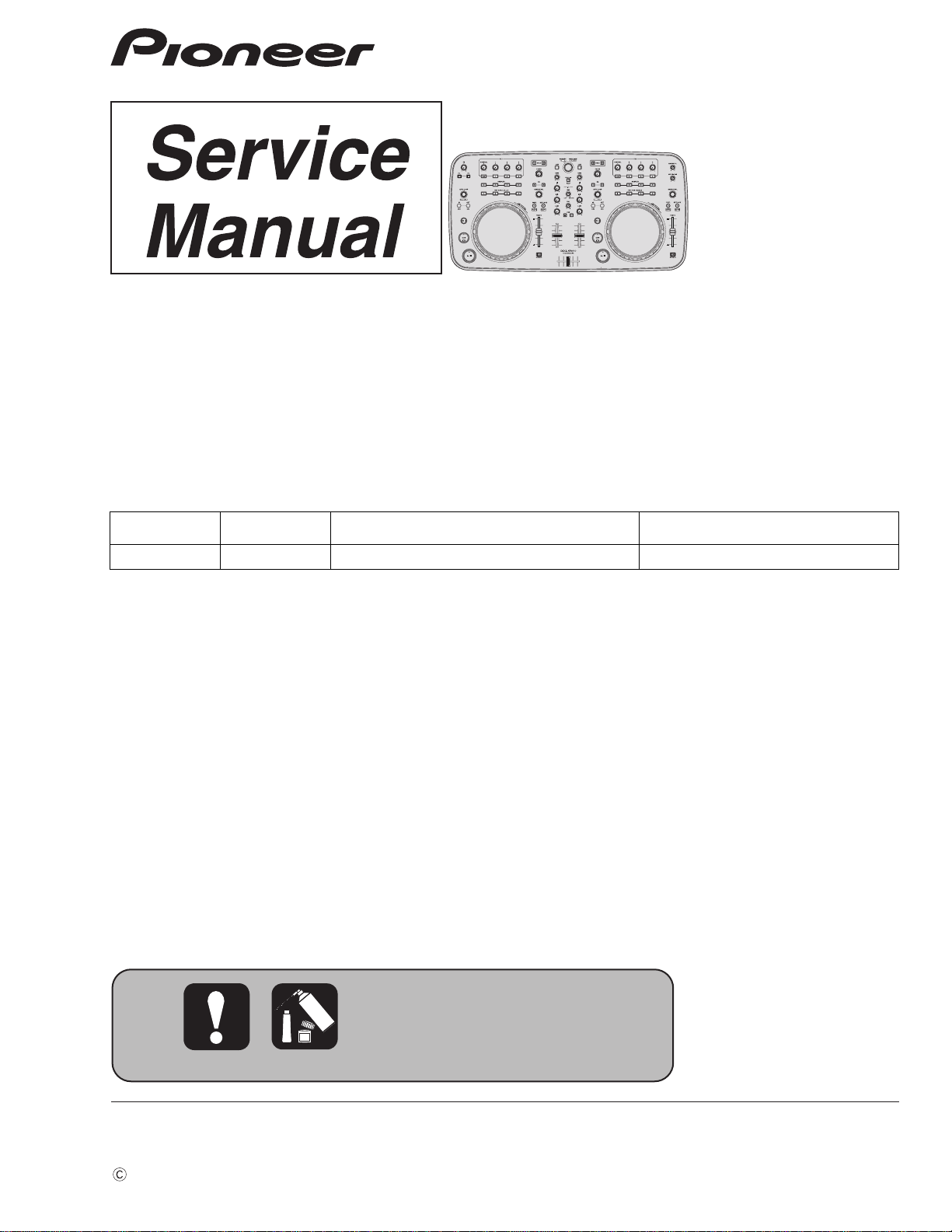
DJ Controller
DDJ-ERGO-V
THIS MANUAL IS APPLICABLE TO THE FOLLOWING MODEL(S) AND TYPE(S).
Model Type Power Requirement Remarks
DDJ-ERGO-V XJ5 DC 5 V
ORDER NO .
RRV4269
PIONEER CORPORATION 1-1, Shin-ogura, Saiwai-ku, Kawasaki-shi, Kanagawa 212-0031, Japan
PIONEER ELECTRONICS (USA) INC. P.O. Box 1760, Long Beach, CA 90801-1760, U.S.A.
PIONEER EUROPE NV Haven 1087, Keetberglaan 1, 9120 Melsele, Belgium
PIONEER ELECTRONICS ASIACENTRE PTE. LTD. 253 Alexandra Road, #04-01, Singapore 159936
PIONEER CORPORATION
K-IZV NOV.
2011 Printed in Japan
Page 2

1
WARNING
This product may contain a chemical known to the State of California to cause cancer, or birth defects or other reproductive
harm.
Health & Safety Code Section 25249.6 - Proposition 65
This service manual is intended for qualified service technicians; it is not meant for the casual do-ityourselfer. Qualified technicians have the necessary test equipment and tools, and have been trained
to properly and safely repair complex products such as those covered by this manual.
Improperly performed repairs can adversely affect the safety and reliability of the product and may
void the warranty. If you are not qualified to perform the repair of this product properly and safely, you
should not risk trying to do so and refer the repair to a qualified service technician.
2 3 4
SAFETY INFORMATION
A
B
C
D
E
F
2
1
2 3 4
DDJ-ERGO-V
Page 3

5
6 7 8
CONTENTS
SAFETY INFORMATION..........................................................................................................................................................2
1. SERVICE PRECAUTIONS....................................................................................................................................................4
1.1 NOTES ON SOLDERING. .......................................... .......................................... ..........................................................4
1.2 SERVICE NOTICE............................................................................................. .............................................................4
2. SPECIFICATIONS.................................................................................................................................................................5
3. BASIC ITEMS FOR SERVICE..............................................................................................................................................6
3.1 CHECK POINTS AFTER SERVICING ............................. .......................................... ....................................................6
3.2 JIGS LIST.......................................................................................................................................................................6
3.3 PCB LOCATIONS............................................... ... .......................................... ...............................................................7
4. BLOCK DIAGRAM................................................................................................................................................................8
4.1 OVERALL WIRING DIAGRAM ................................................................................................. ......................................8
4.2 OVERALL BLOCK DIAGRAM............................. .......................................... ................................................................10
4.3 POWER BLOCK DIAGRAM .................................. .. .......................................... ...........................................................12
5. DIAGNOSIS........................................................................................................................................................................14
5.1 POWER ON SEQUENCE............................................................................. ................................................................14
5.2 TROUBLESHOOTING............ .......................................... .......................................... ..................................................16
5.3 VOLTAGE MONITORING.............................................................................. ................................................................25
5.4 ABOUT POWER-SAVING MODE...................................................................... ...........................................................26
5.5 OPERATION CHECK METHODS, USING VIRTUAL DJ................................................. .............................................27
6. SERVICE MODE.................................................................................................................................................................30
6.1 HOW T O ENTER EACH MODE ........................................................................ ... ... .....................................................30
6.2 FIRMWARE VERSION CONFIRMATION METHODS..................................................................................................31
6.3 SERVICE MODE.................................................................................... ......................................................................33
6.4 FACTORY RESET MODE.............................................................................................................................................36
6.5 POWER-SAVING MODE......................................... ... .......................................... ........................................................37
6.6 ERROR DISPLAY.........................................................................................................................................................37
6.7 ABOUT THE DEVICE......................................... .......................................... ................................................................37
7. DISASSEMBLY ...................................................................................................................................................................38
8. EACH SETTING AND ADJUSTMENT................................................................................................................................43
8.1 NECESSARY ITEMS TO BE NOTED...........................................................................................................................43
8.2 HOW T O PROGRAM COPY FOR USB CONTROLLER..................... ... ... ... ................................................ .. ... ...........43
8.3 HOW TO FIRMWARE UPDATE.................................. .......................................... ........................................................44
8.4 JOG DIAL ROTATION LOAD ADJUSTMENT...................................... ................................................ ... ......................45
9. EXPLODED VIEWS AND PARTS LIST...............................................................................................................................46
1 PACKING SECTION........................................... ... .......................................... .............................................................46
9.
9.2 EXTERIOR SECION............................. .......................................... ..............................................................................48
9.3 CONTROL PANEL SECTION....................... .......................................... ......................................................................50
9.4 JOG SECTION ................. ... .......................................... .......................................... .....................................................52
10. SCHEMATIC DIAGRAM......................................................................... .. .........................................................................54
10.1 JACK ASSY................................................................................................................................................................54
10.2 IFPW ASSY (1/3) and HPLC ASSY............................................................................................................................56
10.3 IFPW ASSY (2/3)........................................................................................................................................................58
10.4 IFPW ASSY (3/3)........................................................................................................................................................60
10.5 CDJ1 ASSY (1/2) ........................................................................................................................................................62
10.6 CDJ1 ASSY (2/2) ........................................................................................................................................................64
10.7 HPJK and CRFD ASSYS............................................................................................................................................66
10.8 CDJ2 ASSY (1/2) ........................................................................................................................................................67
10.9 CDJ2 ASSY (2/2) ........................................................................................................................................................68
10.10 JOG1 and JOG2 ASSYS..........................................................................................................................................70
10.11 TCH1 and TCH2 ASSYS..........................................................................................................................................71
10.12 VOLTAGES ...............................................................................................................................................................72
10.13 WAVEFORMS...........................................................................................................................................................73
11. PCB CONNECTION DIAGRAM..................... ... ... ................................................ .. ...........................................................78
11.1 JACK ASSY................................................................................................................................................................78
11.2 IFPW , HPLC and HPJK ASSYS.................................................................................................................................82
11.3 CDJ1 and CRFD ASSYS............................................................................................................................................86
11.4 CDJ2 ASSY................................................................................................................................................................90
11.5 JOG1, JOG2, TCH1 and TCH2 ASSYS.....................................................................................................................94
12. PCB PARTS LIST............................................................ .......................................... ........................................................95
A
B
C
D
E
F
DDJ-ERGO-V
5
6 7 8
3
Page 4

1
• For environmental protection, lead-free solder is used on the printed circuit boards mounted in this unit.
Be sure to use lead-free solder and a soldering iron that can meet specifications for use with lead-free solders for repairs
accompanied by reworking of soldering.
• Compared with conventional eutectic solders, lead-free solders have higher melting points, by approximately 40 ºC.
Therefore, for lead-free soldering, the tip temperature of a soldering iron must be set to around 373 ºC in general, although
the temperature depends on the heat capacity of the PC board on which reworking is required and the weight of the tip of
the soldering iron.
Do NOT use a soldering iron whose tip temperature cannot be controlled.
Compared with eutectic solders, lead-free solders have higher bond strengths but slower wetting times and higher melting
temperatures (hard to melt/easy to harden).
The following lead-free solders are available as service parts:
• Parts numbers of lead-free solder:
GYP1006 1.0 in dia.
GYP1007 0.6 in dia.
GYP1008 0.3 in dia.
Voltage Monitoring
This unit always monitors for power failure and will shut itself off immediately after an error is detected.
A power failure is indicated with flashing of the illumination LED of the channel fader for left side deck (deck A or C).
Other LEDs are unlit after an error is generated.
After the unit shuts itself off because of an error, disconnect the USB cable and wait at least 1 minute before
turning the unit back on.
Repair the unit according to the diagnostic procedures described in “5.3 VOLTAGE MONITORING.”
On Point-of-Sale Demo Mode
This product is provided with a Demo mode to be used when displayed on a stand in a shop.
Demonstrations with lighting of the LEDs on the control panel are automatically performed even if this product is connected
with a PC without the DJ application (VIRTUAL DJ LE) being started on the PC.
This mode will be established if no transmission or reception of MIDI signals is performed for 1 minute after the controller is
turned ON.
After VIRTUAL DJ LE is started, Normal Operation mode will be entered.
On the EEPROM on the IFPW ASSY
No program has been stored in the EEPROM (IC104) on the IFPW Assy (blank ROM) when it is supplied as a part for service.
After the EEPROM is replaced, be sure to copy the program for the USB controller to it. For details, see “8.2 HOW TO
PROGRAM COPY FOR USB CONTROLLER.”
2 3 4
1. SERVICE PRECAUTIONS
1.1 NOTES ON SOLDERING
A
B
C
D
1.2 SERVICE NOTICE
E
F
4
1
2 3 4
DDJ-ERGO-V
Page 5

5
General – Main Unit
Power supply.............................................................DC 5 V
Power consumption ..................................................500 mA
Main unit weight..............................................2.9 kg (6.4 lb)
Max. dimensions
.................. 554.8 mm (W) × 103.2 mm (H) × 279.8 mm (D)
(21.8 in. (W) × 4.1 in. (H) × 11 in. (D))
Tolerable operating temperature
......................................+5 °C to +35 °C (+41 °F to +95 °F)
Tolerable operating humidity
............................................5 % to 85 % (no condensation)
Audio Section
Rated output level
MASTER OUT 1..................................................4.2 Vrms
MASTER OUT 2..................................................2.1 Vrms
Total harmonic distortion
MASTER OUT 1...................................................0.006 %
MASTER OUT 2...................................................0.006 %
Frequency characteristic
MASTER OUT 1.......................................20 Hz to 20 kHz
MASTER OUT 2.......................................20 Hz to 20 kHz
S/N ratio (when playing on computer)
MASTER OUT 1..........................101 dB (at rated output)
MASTER OUT 2..........................101 dB (at rated output)
Input impedance
AUX..........................................................................24 kΩ
MIC...........................................................................11 kΩ
Output impedance
MASTER OUT 1.............................................1 kΩ or less
MASTER OUT 2.............................................1 kΩ or less
PHONES........................................................10 Ω or less
Input / Output terminals
USB terminal
B type...................................................................... 1 set
MASTER OUT 1 output terminal
TRS phone jack (Ø 6.3 mm).................................... 1 set
MASTER OUT 2 output terminal
RCA pin jacks..........................................................1 set
PHONES output terminal
Stereo phone jack (Ø 6.3 mm) ................................ 1 set
Stereo mini phone jack (Ø 3.5 mm)......................... 1 set
AUX input terminal
RCA pin jacks..........................................................1 set
MIC input terminal
Phone jack (Ø 6.3 mm)............................................ 1 set
For improvement purposes, specifications and design of this
unit and the included software are subject to change without
notice.
• USB cable
(DDE1128)
• VIRTUAL DJ LE software CD-ROM
(DXX2685)
• Driver software/operating instructions CD-ROM
(DRU1001)
• Read Before Use (Important)
(DRH1122)
• Quick Start Guide
(DRH1123)
• Hardware Diagram for Virtual DJ (Table of Supported Functions)
(DRH1124)
• Warranty card
• Service network list (for Japanese customers)
Accessories
2. SPECIFICATIONS
6 7 8
A
B
C
D
5
DDJ-ERGO-V
6 7 8
E
F
5
Page 6
1
Items to be checked after servicing
To keep the product quality after servicing, confirm recommended check points shown below.
No. Procedures Check points
1
Confirm that the customer complaint has been resolved.
If the problem pointed out by the customer occurs with a specific
source or operation, such as PC input, AUX/MIC input, Fader, or
Volume, input that specific source then perform that specific
operation for checking.
The customer complain must not be reappeared.
Audio and operations must be normal.
2
Confirmation of operation of operating elements
Enter Service mode.
There must be no errors in operations of each button, Rotary
selector, Volume, Fader, Slider and JOG.
3
Check the analog audio output.
Connect this unit with a PC with the DJ application (Virtual DJ LE)
installed, via USB, then operate the DJ application (Virtual DJ LE).
There must be no errors, such as noise, in audio signals and
operations of the MASTER/HEADPHONES outputs.
4
Check the analog audio input.
Input an audio signal via AUX/MIC.
Audio and operations must be normal.
5 Check the appearance of the product. No scratches or dirt on its appearance after receiving it for service.
Item to be checked regarding audio
Distortion
Noise
Volume too low
Volume too high
Volume fluctuating
Sound interrupted
See the table below for the items to be checked regarding audio.
Lubricants and Glues List
Name Part No. Remarks
Lubricating oil GYA1001 Refer to “9.4 JOG SECTION”.
Jigs List
Jig Name Part No. Purpose of use / Remarks
USB cable GGP1193 for PC connection
2 3 4
3. BASIC ITEMS FOR SERVICE
3.1 CHECK POINTS AFTER SERVICING
A
B
C
D
3.2 JIGS LIST
E
F
6
1
2 3 4
DDJ-ERGO-V
Page 7
5
NSP 1..PLMX ASSY DWM2450
2..JOG1 ASSY DWS1436
2..TCH1 ASSY DWS1437
2..JOG2 ASSY DWS1438
2..TCH2 ASSY DWS1439
2..CDJ1 ASSY DWX3302
2..HLD1 ASSY DWX3309
2..HLD2 ASSY DWX3310
NSP 1..PLJK ASSY DWM2451
2..CDJ2 ASSY DWX3303
2..JACK ASSY DWX3304
2..CRFD ASSY DWX3305
2..HPJK ASSY DWX3306
2..HLD3 ASSY DWX3311
2..HPLC ASSY DWX3324
1..IFPW ASSY DWX3301
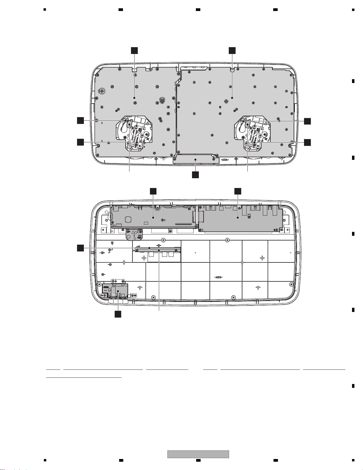
Mark No. Description Part No. Mark No. Description Part No.
LIST OF ASSEMBLIES
NOTES: - Parts marked by “NSP” are generally unavailable because they are not in our Master Spare Parts List.
-
The > mark found on some component parts indicates the importance of the safety factor of the part.
Therefore, when replacing, be sure to use parts of identical designation.
E
HPJK ASSY
F
CRFD ASSY HLD1 ASSYHLD2 ASSY
HLD3 ASSY
H
JOG1 ASSY
J
TCH1 ASSY
B
IFPW ASSY
A
JACK ASSY
D
CDJ1 ASSY
G
CDJ2 ASSY
• Bottom view
C
HPLC ASSY
I
JOG2 ASSY
K
TCH2 ASSY
3.3 PCB LOCATIONS
6 7 8
A
B
C
5
6 7 8
DDJ-ERGO-V
D
E
F
7
Page 8
1
A
JACK ASSY
(DWX3304)
F
CRFD ASSY
(DWX3305)
Either the JOG1 Assy or JOG2 Assy is assembled here. The JOG1 Assy and
JOG2 Assy are interchangeably used and handled similarly in their production
management.
Either the TCH1 Assy or TCH2 Assy is assembled here. The TCH1 Assy and
TCH2 Assy are interchangeably used and handled similarly in their production
management.
DCS1115-A
VR2901
1
324
5
JA294
DKN1622-A
231
JA2901
DKN1614-A
2
3
1
JA2903
AKB7181-A
543
2
1
DCS1111-A
VR2902
1
3
2
S2901
DSH1025-A
123
JA2902
AKB7181-A
54321
51048-0300
JH1002
1
V+3R3_AD
2
AD_CRSFD
3
GND_AD
CN2801
52151-0310
1
GND_D
2
JOG_TCH1/2
3
V+3R3_UCOM
PF04PG-B05
CN2701
1
GND_D2V+3R3_UCOM
3
JOG_DIAL1/2_0
4
JOG_DIAL1/2_1
JA2905
DKN1622-A
231
AKF7002-A
KN2903
1
AKF7002-A
KN1501
1
AKF7002-A
KN1001
1
KN2902
VNE1948-A
GND1
1
GND2
2
GND3
3
GND4
4
VKN1842-A
CN101
1
MIC_AUXIN_L
2
GND_AI
3
MIC_AUXIN_R
4
V-6_J
5
V+7_J
6
GND_AI
7
GND_AI
8
GND_AI
9
GND_AO
10
GND_AO
11
MASTER1_L+
12
GND_AO
13
MASTER1_L-
14
GND_AO
15
MASTER2_L
16
GND_AO
17
GND_AO
18
GND_AO
19
MASTER2_R
20
GND_AO
21
MASTER1_R+
22
GND_AO
23
MASTER1_R-
24
GND_AO
25
MUTE
26
MIC_AUXIN_SW
27
MIC_AUXIN_SEL
VKN2097-A
CN2001
1
V+3R3_AD
2
GND_AD
3
LED_8
4
LED_7
5
LED_9
6
ENC_ABL2_0
7
LED_10
8
ENC_ABL2_1
9
LED_11
10
ENC_V OL2_0
11
LED_12
12
ENC_V OL2_1
13
KEY_IN_7
14
SW_AD_B
15
KEY_IN_6
16
AD_PTCHFD2_1
17
KEY_IN_5
18
AD_PTCHFD2_2
19
KEY_IN_4
20
LED_14
21
GND_D
22
AD_FX2
23
GND_D
24
AD_VOL2
25
V+3R3_UCOM
26
SW_AD_A
27
GRID_7
28
JOG_TCH2
29
GRID_6
30
JOG_DIAL2_0
31
GRID_5
32
JOG_DIAL2_1
33
GRID_4
34
GRID_0
35
GRID_3
36
GRID_1
37
GRID_2
38
GND_LED
39
V+5_LED
VKN2097-A
CN1003
1
V+5_LED
2
GND_LED
3
GRID_2
4
GRID_1
5
GRID_3
6
GRID_0
7
GRID_4
8
JOG_DIAL2_1
9
GRID_5
10
JOG_DIAL2_0
11
GRID_6
12
JOG_TCH2
13
GRID_7
14
SW_AD_A
15
V+3R3_UCOM
16
AD_VOL2
17
GND_D
18
AD_FX2
19
GND_D
20
LED_14
21
KEY_IN_4
22
AD_PTCHFD2_2
23
KEY_IN_5
24
AD_PTCHFD2_1
25
KEY_IN_6
26
SW_AD_B
27
KEY_IN_7
28
ENC_V OL2_1
29
LED_12
30
ENC_V OL2_0
31
LED_11
32
ENC_ABL2_1
33
LED_10
34
ENC_ABL2_0
35
LED_9
36
LED_7
37
LED_8
38
GND_AD
39
V+3R3_AD
CN2002
KM200NA4L
1
GND_D
2
V+3R3_UCOM
3
JOG_DIAL2_04JOG_DIAL2_1
51048-0300
JH2001
1
GND_D
2
JOG_TCH2
3
V+3R3_UCOM
51048-0300
CN2601
1
V+3R3_AD
2
AD_CRSFD
3
GND_AD
VKN2097-A
CN1004
1
V+3R3_UCOM2GND_D3VBUS_DET
4
GND_D
5
A_MUTE6USB_CTRL17FAULT_DET28USB_XRST9PWR_ON10USB_ERR11FAULT_DET12MIC AUXIN SW
VKN1842-A
CN2901
1
MIC_AUXIN_SEL
2
MIC_AUXIN_SW
3
MUTE
4
GND_AO
5
MASTER1_R-
6
GND_AO
7
MASTER1_R+
8
GND_AO
9
MASTER2_R
10
GND_AO
11
GND_AO
12
GND_AO
13
MASTER2_L
14
GND_AO
15
MASTER1_L-
16
GND_AO
17
MASTER1_L+
18
GND_AO
19
GND_AO
20
GND_AI
21
GND_AI
22
GND_AI
23
V+7_J
24
V-6_J
25
MIC_AUXIN_R
26
GND_AI
27
MIC_AUXIN_L
VKN2097-A
CN102
28
MIC AUXIN SW
29
FAULT_DET
30
USB_ERR
31
PWR_ON
32
USB_XRST
33
FAULT_DET2
34
USB_CTRL1
35
A_MUTE
36
GND_D
37
VBUS_DET
38
GND_D
39
V+3R3_UCOM
AKF7002-A
KN2901
1
AUX IN VOL
MIC IN
AUX IN
MIC IN VOL
MASTER2
MIC/AUX SELECT
MASTER1_R
MASTER1_L
VERTICAL
CONTACTSIDE
VERTICAL
CONTACTSIDE
VERTICAL
VERTICAL
CONTACTSIDE
CONTACTSIDE
VERTICAL
VERTICAL
CONTACTSIDE
HORIZONTAL
LENGTH=70mm
DDD1585PITCH=1mm
SAME FACE
FFC 27P
FFC 39P
PITCH=1mm
SAME FACE
DDD1587LENGTH=125mm
D20PDY0305E
LENGTH=50mm
PITCH=2mm
PARALLEL JUMPER WIRE
LR
RL
VERTICAL
LENGTH=100mm
CONNECTOR ASS'Y
D20PDY0310E
HORIZONTAL
VERTICAL
PITCH=2mm
PARALLEL JUMPER WIRE
HORIZONTAL
LENGTH=50mm
HLD1/2 ASSY
DWX3309/3310- /J
BOARD IN - PH
CONTACTSIDE
CDJ1
(DWX
D
CDJ2 ASSY
(DWX3303)
G
G G
1/2, 2/2
J K
TCH1 ASSY/TCH2 ASSY
(DWS1437/DWS1439)
/
H I
JOG1 ASSY/JOG2 ASSY
(DWS1436/DWS1438)
/
-
-
-
Either
JOG2
manag
2 3 4
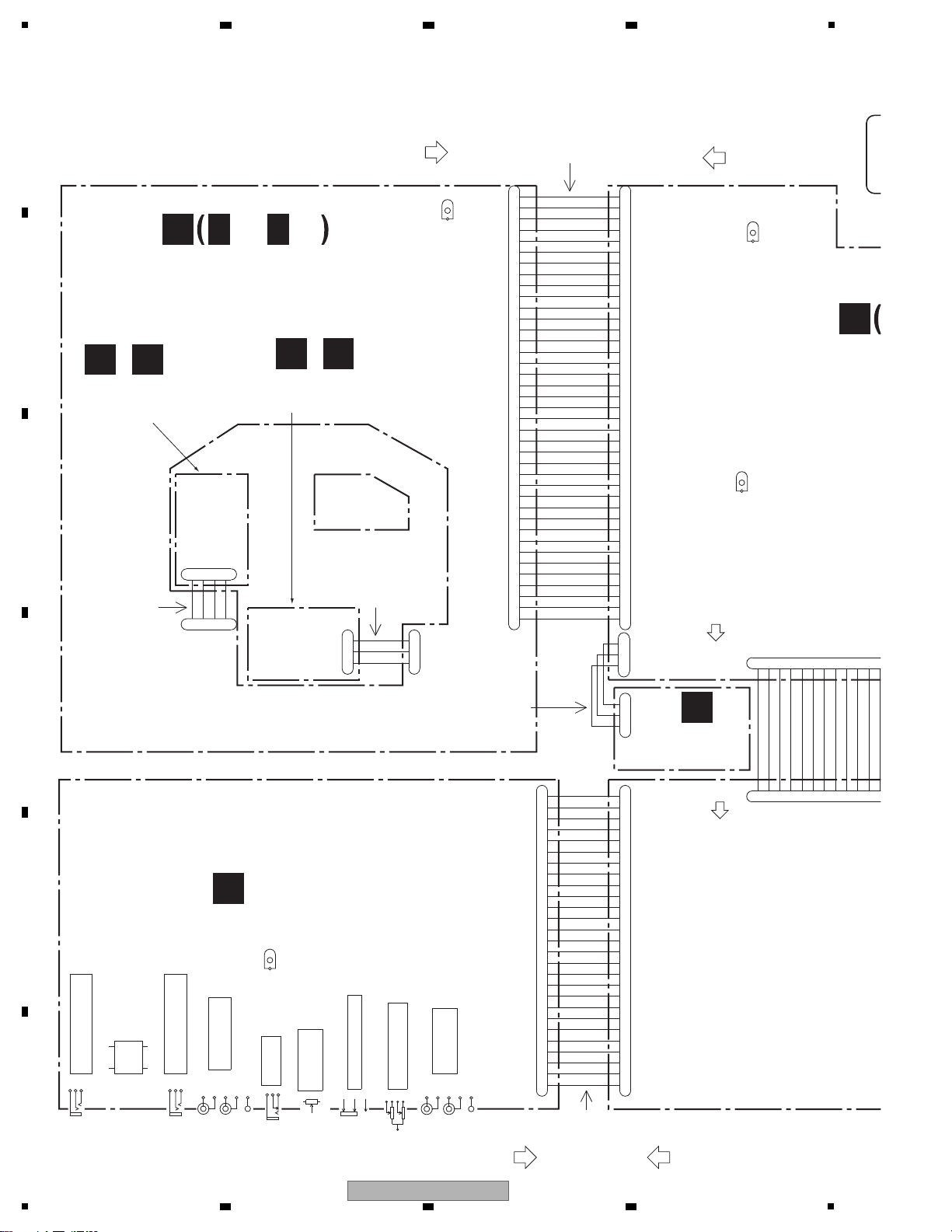
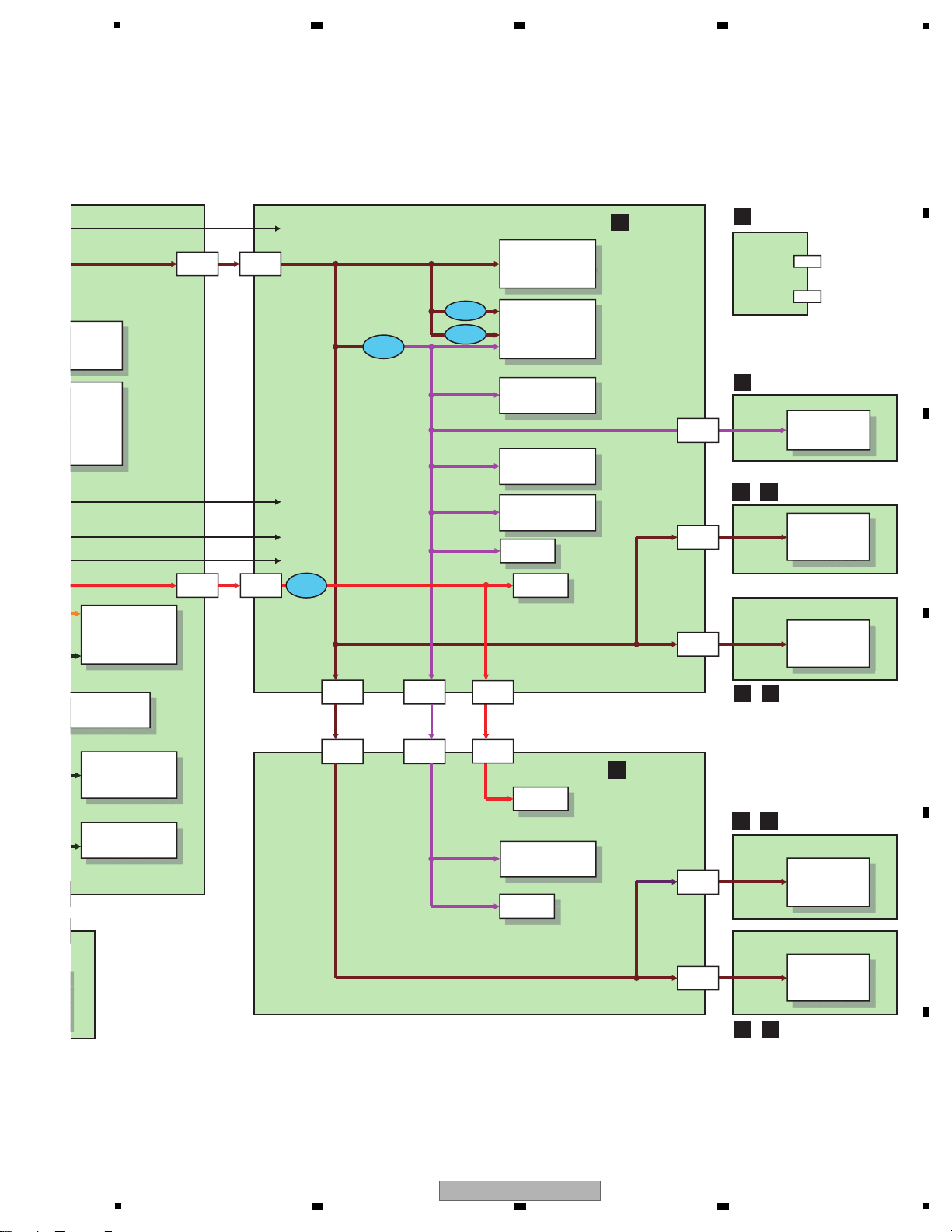
4. BLOCK DIAGRAM
4.1 OVERALL WIRING DIAGRAM
A
B
C
D
E
F
8
1
2 3 4
DDJ-ERGO-V
Page 9
5
E
HPJK ASSY
(DWX3306)
C
HPLC ASSY
(DWX3324)
H I
JOG1 ASSY/JOG2 ASSY
(DWS1436/DWS1438)
/
J K
TCH1 ASSY/TCH2 ASSY
(DWS1437/DWS1439)
/
CN1801
52151-0310
1
GND_D
2
JOG_TCH1/2
3
V+3R3_UCOM
PF04PG-B05
CN1701
1
GND_D
2
V+3R3_UCOM
3
JOG_DIAL1/2_0
4
JOG_DIAL1/2_1
DKN1237-A
JA102
123
4
RT1
RT2
CN103
52147-0510
1
GND_F22GND_F2
3
HP_L
4
GND_AH
5
HP_R
JA1901
DKN1622-A
231
S101
DSH1025-A
123
KN101
VNE1948-A
GND1
1
GND2
2
GND3
3
GND4
4
CN104
52151-0310
1
V+5_HP
2
GND_D
3
V+5_HP_OUT
CN1001
NM
1
DBG_CNVSS
2
MAIN_XRST
3
GND_D
4
V+3R3_UCOM
CN1002
KM200NA4L
1
GND_D
2
V+3R3_UCOM
3
JOG_DIAL1_04JOG_DIAL1_1
51048-0300
JH1001
1
GND_D
2
JOG_TCH1
3
V+3R3_UCOM
3
VBUS_DET
4
GND_D
5
A_MUTE6USB_CTRL17FAULT_DET28USB_XRST9PWR_ON10USB_ERR11FAULT_DET12MIC_AUXIN_SW13ADC_DAC_XRST
14
MIC_AUXIN_SEL15USB_BUSY16USB_REQ17MIC_AUXIN_MUTE18GND_D19EEP_SCL20GND_D
21
EEP_SDA22GND_D
23
GND_D24GND_D25PWR_SW26GND_D27DAC_CDTI28GND_D29DAC_CS30GND_D31DAC_CCLK32GND_D33USB_CTRL234GND_D35GND_D36GND_LED37V+5_LED38GND_LED39V+5_LED
51048-0300
JH3001
1
V+5_HP2GND_D3V+5_HP_OUT
51048-0500
JH1901
1
GND_F22GND_F2
3
HP_L4GND_AH5HP_R
1
V+5_LED
2
GND_LED
3
V+5_LED
4
GND_LED
5
GND_D6GND_D
7
USB_CTRL2
8
GND_D
9
DAC_CCLK
10
GND_D
11
DAC_CS
12
GND_D
13
DAC_CDTI
14
GND_D
15
PWR_SW
16
GND_D17GND_D18GND_D
19
EEP_SDA
20
GND_D
21
EEP_SCL
22
GND_D
23
MIC_AUXIN_MUTE
24
USB_REQ
25
USB_BUSY
26
MIC_AUXIN_SEL
27
ADC_DAC_XRST
28
MIC_AUXIN_SW
29
FAULT_DET
30
USB_ERR
31
PWR_ON
32
USB_XRST
33
FAULT_DET2
34
USB_CTRL1
35
A_MUTE
36
GND_D
37
VBUS_DET
KN1901
VNE1948-A
GND1
1
GND2
2
GND3
3
GND4
4
JA1902
XKN3017-A
2
3
1
FOR UCOM DEBUG
VERTICAL
VERTICAL
VERTICAL
HORIZONTAL
DDD1586LENGTH=325mm
PITCH=1mm
FFC 39P
SAME FACE
PITCH=2mm
LENGTH=200mm
PARALLEL JUMPER WIRE
D20PDY0520E
D20PDY0310E
PITCH=2mm
PARALLEL JUMPER WIRE
LENGTH=100mm
HP JACK
Mini JACK
DWX3309/3310- /J
HLD1/2 ASSY
LENGTH=50mm
BOARD IN - PH
HORIZONTAL
CONNECTOR ASS'Y
HLD3 ASSY DWX3311- /J
PITCH=2mm
LENGTH=100mm
PARALLEL JUMPER WIRE
D20PDY0310E
USB-B JACK
POWER SW
CDJ1 ASSY
(DWX3302)
D
D D
1/2, 2/2
IFPW ASSY
(DWX3301)
B
B B
1/3- 3/3
-
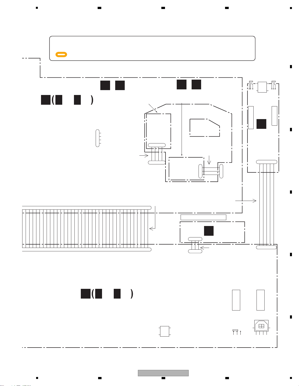
When ordering service parts, be sure to refer to "EXPLODED VIEWS and PARTS LIST" or "PCB PARTS LIST".
-
The > mark found on some component parts indicates the importance of the safety factor of the part.
Therefore, when replacing, be sure to use parts of identical designation.
-
: The power supply is shown with the marked box.
Either the JOG1 Assy or JOG2 Assy is assembled here. The JOG1 Assy and
JOG2 Assy are interchangeably used and handled similarly in their production
management.
Either the TCH1 Assy or TCH2 Assy is assembled here. The TCH1 Assy and
TCH2 Assy are interchangeably used and handled similarly in their production
management.
6 7 8
A
B
C
D
5
DDJ-ERGO-V
6 7 8
E
F
9
Page 10
1
CN 2001 CN1003
PC1701 IC1801
LED_7-12,14 LED_0-6,13
/PC2701 /IC2801
VR2206 KEY_IN_4-7 KEY_IN_0-3,7
TEMPO SLIDER GRID_0-7 GRID_0-7
CN1701 CN1801
AD_PTCHFD2_1
/CN2701
/CN2801
AD_PTCHFD2_2
ENC_ABL2_0
ENC_ABL2_1
CN 2002 JH2001 S2225
AUTO LOOP
ENC_VOL2_0
ENC_VOL2_1
S2226
SAMPLE VOL
AD_FX2
AD_VOL2
7
SW_AD_A
SW_AD_B
JOG_TCH2
JOG_DIAL2_1
JOG_DIAL2_0
XIN
XOUT
MAIN_XRST
AD_CRSFD JH1002
CN2601
CN1004
CROSS FADER
CN102
Lch
Rch
A_MUTE
MASTER1_L- L
MASTER1_L+ R
MASTER1_R-
MASTER1_R+
MASTER2_R
MASTER2_L
MUTE
MIC_AUXIN_SW
MIC_AUXIN_SEL
Rch
MIC_AUXIN_R
MIC_AUXIN_L
Lch
CN 2901 CN101
S2901
MASTER1 OUT MASTER2 OUT MIC IN MIC IN VOL MIC/AUX SELECT AUX IN VOL A UX IN
MIC_AUXIN_SEL
MIC_AUXIN_SW
A_MUTE
VR2901 VR2902 JA2902
ADC_DAC_XRST
MIC_AUXIN_MUTE
DAC CS
JA2904
JA2905
JA2903
JA2901
132
3
2
3
2
13
6217
IC507
627
1
IC506
537
1
IC505
IC501
DAC
1
1
1
1
2
2
1
2
2
2
3
1
13
IC2902
3
5
1
7
IC2901
IC2903
IC2904
5
5
2
7
2
7
111111
2
2
3
1
2
1
1
5
7
9
1
MUTE CIRCUIT
1
IC502
DAC
IC504
113
5
1
7
IC503
ADC
1
2
MUTE
CIRCUIT
34 2
34 2
3
3
2
IC2201
SW IC
VOL
MATRIX
Circuit
KEY
LED
ROTARY
ROTARY
1
32
2
2
1
1
9
1
14
2
6
82
1
1
12
1
2
1
2
2
2
MATRIX
Circuit
1
8
1
1
1
1
2
2
2
3
3
3
2
IC
UCO
2
2
2
8
8
10
8
9
9
7
8
8
8
9
91
322
1
232
511
4
333
124
2
1
2
5678
5678
5
IC1001
Reset IC
1
X1001
4MHz CERAMIC
RESONATOR
11
MUTE
CIRCUIT
H
G
CDJ2 ASSY
F
CRFD ASSY
A
JACK ASSY
D
CDJ1 ASSY
I
JOG1/2 ASSY
/
J K
TCH1/2 ASSY
/
2 3 4
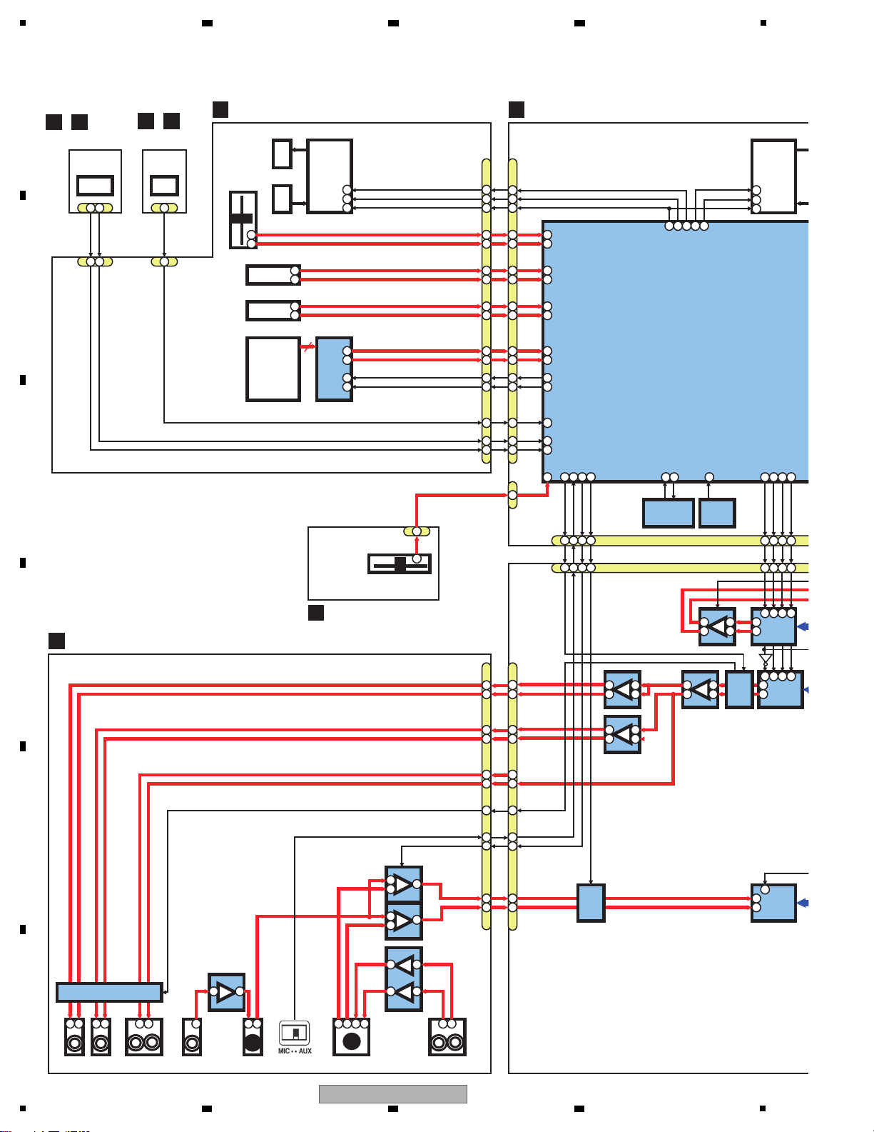
4.2 OVERALL BLOCK DIAGRAM
A
B
C
D
E
F
10
DDJ-ERGO-V
1
2 3 4
Page 11
5
CH FADER A CH FADER B
VR1208 VR1213
PC1701 IC1801
/PC2701 /IC2801
RID_0-7 TEMPO SLIDER
AD_FADER_A
AD_FADER_B
CN1701 CN1801
/CN2701 /CN2801
S1234
BROWSE CN1002 JH1001
S1232
AUTO LOOP
JA1901
JA1902
S1233
SAMPLE VOL
HP JACK
Mini JACK
8
8
JH1901
HP_L HP_R
JOG_DIAL1_0
JOG_DIAL1_1
JOG_TCH1
AIN_XRST
JH3001
CN103
CN104
Lch
Rch
XIN XOUT
P_SW
S101
JA102
POWER SW
PWR_SW
USB_DP
ADC_DAC_XRST
DAC_CCLK
DAC_CS
DAC_CDTI
FAULT_DET
FAULT_DET 2
USB_CTRL2
USB_BUSY
USB_ERR
USB_CTRL1
USB_REQ
VBUS_DET
EEP_SDA
USB_XRST
PWR_ON
EEP_SCL
USB_DN
IC102
USB uCom
TUSB3200A
3
32
32
5
34 2
34 2
35
Cap
IC501
DAC
1
1
IC502
DAC
113
5
IC503
ADC
1
2
3
3
3
4
3
3
Master Data
HP Data
MIC/AUX Data
BCL
LRCK
MCLK
78
1
232
1
VOL
MATRIX
Circuit
KEY
LED
ROTARY
ROTARY
IC1201
SW IC
1
3
1
9
4
2
2
1
2
1
IC1201
SW IC
1
3
1
9
IC1002
UCOM IC
6
2
2
8
8
9
9
4
5
1
1
8
8
10
8
91
232
333
2
1
2
Q306
FET
IC307
VBUS
DETECT
VBUS
DETECT
CIRCUIT
3
8
1
2
4
2
1
43
3
6
3
7
3
1
2
1
2
2
1
123921373
3
POWER
DETECT
CIRCUIT
5678
5678
5
001
et IC
IC201
EEPROM
5
6
X101
6MHz Xtal
55
ROTARY
2
14
4
22
99
5V
Discharge
Circit
IC305
REG
IC301
REG
IC303
REG
IC304
REG
IC302
-6V
DDC
55
MUTE
CIRCUIT
3
3
1
AD_FX1
SW_AD_A
AD_MIX1
ENC_VOL1_0
ENC_ABL1_0
ENC_BRWS_0
AD_PITCH1_1
31
31
V+5_HPV+5_HP_OUT
432 4332 31 2114
- B
B
IFPW ASSY
E
HPJK ASSY
C
HPLC ASSY
H I
JOG1/2 ASSY
/
J K
TCH1/2 ASSY
/
6 7 8
A
B
C
D
E
F
5
6 7 8
DDJ-ERGO-V
11
Page 12
1
ON OFF
P_SW to uc
CONT
CONT
FAULT_DET2 to uc
VBUS_DET to uc
FAULT_DET to uc
DC/DC CONVERTER
REGULATOR
USB ucom
IC102
DAC (HP)
IC502
IC501
DAC (MASTER)
IC505
IC506, 507
OPAMP
IC2901, 2902
IC2904
(for MIC/AUX)
V+5_A
IC302
D/D_CONV
V+7
V+VBUS
USB
ADC (MIC/AUX)
IC503
V+7_J
V+7_J
EEPROM
IC104
RESET IC
IC307
V+5_USB
AMP (HP)
MIC
AUX IN
FILTER, COIL, BEADS
V-6_J
V-6_J
V-6_J
V+7_J
V+7_J
V-6_J
3.3V_REG1
IC304
IC303
Q306
V+5_D
L105
L106
L107
GND
PSW
PWRON
V+5_LED
USB BUS POWER
VOLTAGE DETE CT
V+5_D
DISCHARGE
V+5_D
IC301
IC305
V+5_HP
Charge
Capacitor
V+5_HP_OUT
V+VBUS
1
Ω
V+5_HP
OPAMP
(for MIC/AUX)
L501L502
V+3R3_USB
V+5_HP
_OUT
V+5_HP
_OUT
POWER SLIDE SW
POWER FAULT
V-6
B
IFPW ASSY
V+3R3_UCOM
5V→3.3V
NJM2878F3-33
3.3V_REG2
5V→3.3V
NJM2878F3-33
V+3R3_USB
CTF1629-
CTF1629-
CTF1629-
S-80942CNMC-G9C
7V→5V
NJM2878F3-05
5V_REG
7V→5V
5V_REG
NJM2878F3-05
7V→-6V
5V→7V
NJM2392M
ATH1170-
ATH1170-
OPAMP (MASTER2)
NJM4580MD
OPAMP (MASTER1)
NJM4580MD
A
JACK ASSY
MASTER1(TRS)
MASTER2
C
HPLC ASSY
V+5
_HP
V+5
_HP
BH3547F
IC504
AK4387ET
AK4387ET
AK5358AET
TUSB3200A
S-24CS64A0I
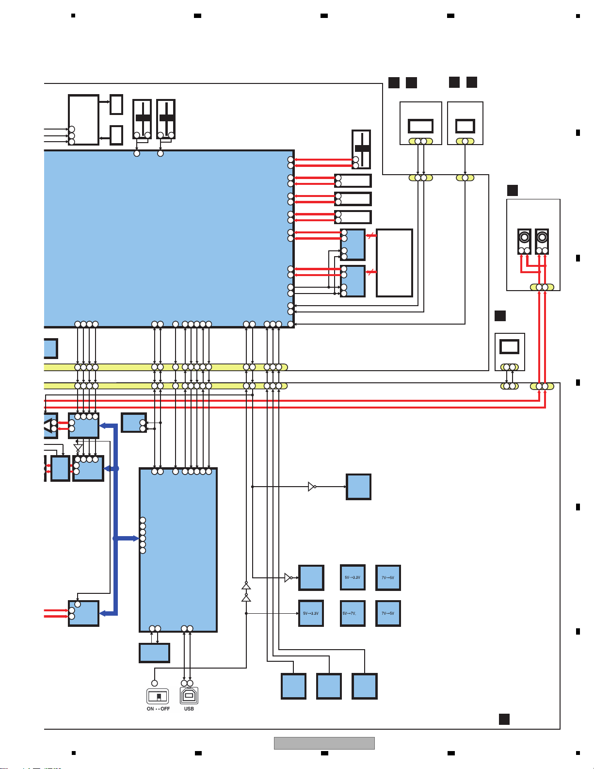
4.3 POWER BLOCK DIAGRAM
A
2 3 4
B
C
D
E
F
12
1
DDJ-ERGO-V
2 3 4
Page 13
P_SW to ucom
HP Jack (Phone)
HP Jack (Mini)
FAULT_DET2 to ucom
VBUS_DET to ucom
FAULT_DET to ucom
MAIN ucom
IC1002
DAC (HP)
IC502
IC501
TEMPO SLIDER
DCV1011
ADC (MIC/AUX)
IC503
CH FADER_A, B
DCV1024
CROSS FADER
DCV1023
V+3R3
_UCOM
V+3R3
_UCOM
V+3R3
_UCOM
V+3R3
_UCOM
V+3R3
_UCOM
V+3R3
_UCOM
VR
LED
V+3R3
_AD
V+3R3
_AD
ANALOG SW
RESET IC
IC1001
L1003
V+3R3_AD
AMP (HP)
V+5_LED
Photointerrupter
Photointerrupter
Photointerrupter
Photointerrupter
V+5
_LED
V+5
_LED
V+5
_LED
V+5
_LED
LED
L1004
V+3R3
_AD
VR
TEMPO SLIDER
DCV1011
CTF1629-
L1001
L1002
D
CDJ1 ASSY
G
CDJ2 ASSY
E
HPJK ASSY
F
CRFD ASSY
H I
JOG1/2 ASSY
/
H I
JOG1/2 ASSY
/
J K
TCH1/2 ASSY
/
J K
TCH1/2 ASSY
/
BH3547F
IC504
AK4387ET
AK4387ET
AK5358AET
DTH1211-
V+3R3
_UCOM
V+3R3
_UCOM
S-80927CNMC-G8X
2.7V DET
R5F3650ENFA-U0
TC74HC4052AF
PC1801/PC2801
GP1S094HCZ0F
PC1801/PC2801
GP1S094HCZ0F
PC1701/PC2701
PC1701/PC2701
SEDS-7573
SEDS-7573
5
6 7 8
A
B
C
D
E
DDJ-ERGO-V
5
6 7 8
F
13
Page 14
1
Y
N
Note: The TUSB3200A is started up after
loading the program from the EEPROM.
Y
N
Y
N
N
Y
Y
N
Note: Start the updating program on the PC.
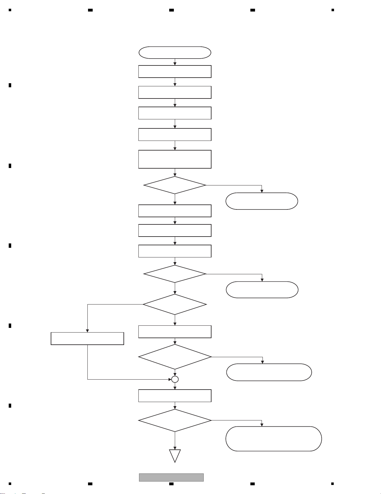
Power ON
Operation clock setting: 32 MHz
Port initial setting
I2C serial initial setting
Peripheral device power: ON
Power failure?
Unit stopped by power failure
Power failure indication by LEDs
Canceling reset of the USB
Controller (TUSB3200A)
Starting opening indication
Checking communication
with the USB controller
Has communication
been established?
Abnormal stopping of the TUSB3200A
LED indication for USB controller error
CRC check of the main flash
CRC error?
(FLASH NG?)
Waiting until power supply
stabilizes then performing
power-failure detection
Finishing opening indication
Unit stopped by power failure
Power failure indication by LEDs
Power voltage
< 4.2 V?
Resetting the USB Controller
(TUSB3200A)
Waiting for a recovery/updating request
LED indication for flash ROM error
Power failure?
A
5. DIAGNOSIS
5.1 POWER ON SEQUENCE
A
B
2 3 4
C
D
E
F
14
1
DDJ-ERGO-V
2 3 4
Page 15
5
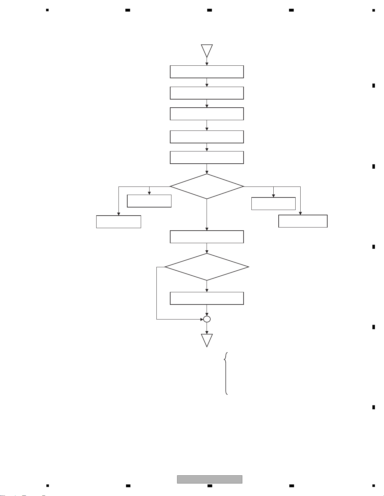
Normal mode
N
Y
* To normal main loop processing
• Power failure monitoring/Power voltage monitoring
• Power ON/OFF SW monitoring
• MIC/AUX switching
• Detection of change in operating elements
• DAC control
• USB transmission (transmission of operating element data)
• USB reception (reception and indication of display data)
Interruption initial setting
Serial communication
initial setting
Timer initial setting
A/D conversion initial setting
MIC/AUX initial setting
Operation mode
judgment
Service mode
(Test mode)
JOG Load
Measurement mode
Display initial setting
DAC initial setting
A
Mode for version
confirmation
Factory Reset
mode
Has reset of the USB
Controller been canceled?
6 7 8
A
B
C
D
E
F
DDJ-ERGO-V
5
6 7 8
15
Page 16
1
[0] Prior Confirmation
[0-1] Checking in Service Mode
[0] Prior Confirmation
[0-1] Checking in Service Mode
[0-2] Checking Internal Cables
[1] Failure in Startup (Failure in power-on)
[1-1] Failure in the power system
[1-2] Failure in the microcomputer system
[2] Display (LED indicators)
[2-1] Any one of the LEDs does not light.
[2-2] Several LEDs do not light or abnormal light
[3] Operations (Buttons/Rotary selectors/Volumes/Faders
/Sliders/JOG)
[3-1] The buttons are disabled.
[3-2] Rotary selector not controllable
[3-3] VRs or faders or sliders not controllable
[3-4] Abnormalities regarding the JOG
[4] USB connection
[4-1] The unit cannot be recognized by the PC when
connected to the PC via USB connection.
[5] AUDIO OUT
[5-1] The MASTER OUT1/MASTER OUT2 is not output.
[5-2] The HEAD PHONE signal is not output.
[6] AUDIO IN
[6-1] The input signal to AUX/MIC is not output
[7] Basic Operation Check of the MAIN UCOM
1 ——— Service mode Identify a failure point. After a failure point is identified, see the section
referenced in this manual.
6. SERVICE MODE
[0-2] Checking Internal Cables
1 Disconnection,
breakage, or
loose connection
of internal cables
Cables Check that all the cables are securely
connected. Check that there is no
breakage in the cables.
Securely connect a cable if it is not connected.
If a cable is broken, replace it.
Note: If an FFC cable is disconnected, be careful of
the orientation of the contacts when reconnecting it,
referring to the printed guide on the board.
4.1 OVERALL
WIRING DIAGRAM
Contents
[1] Failure in Startup (Failure in power-on)
[1-1] Failure in the power system
1 Failure in the
power system (1)
LED indications of
the unit
Set the POWER switch to ON.
Check if the CH Fader LED on the left
deck is flashing.
If it is, power failure in other than V+VBUS and
V+3R3_UCOM is suspected.
See “6 Failure in the power system (2)” in this
table.
4.3 POWER BLOCK
DIAGRAM
5.3 VOLTAGE
MONITORING
2 Failure in USB-
bus power
IFPW Assy
V+VBUS
Set the POWER switch to OFF.
Check that the voltage of the V+VBUS
power line is in the range of 4.75–5.25 V.
If the voltage is outside the range of 4.75–5.25 V,
failure in the USB-bus power and its periphery
may be suspected. Check the USB cable and
USB connector.
4.3 POWER BLOCK
DIAGRAM
10.12 VOLTAGES
1
3
Control error of the
V+3R3_UCOM
regulator on the
IFPW Assy
IFPW Assy
CDJ1 Assy
Set the POWER switch to ON.
Check the voltage at Pin 1 (CONT) of the
V+3R3_UCOM regulator.
If the voltage at Pin 1 (CONT) of the
V+3R3_UCOM regulator is low, the S101 power
switch or Q301, or their peripheral circuits may
be defective.
4.3 POWER BLOCK
DIAGRAM
In a case where the unit is not started after the USB cable is connected and the unit is turned ON
No. Cause Diagnostics Point Item to be Checked Corrective Action Reference
No. Cause Diagnostics Point Item to be Checked Corrective Action Reference
No. Cause Diagnostics Point Item to be Checked Corrective Action Reference
5.2 TROUBLESHOOTING
A
2 3 4
B
C
D
E
F
16
1
DDJ-ERGO-V
2 3 4
Page 17
5
6 Power failure (2)
Identification of
defective Assy
JACK Assy
HPJK Assy
HPLC Assy
Disconnect the cables from each Assy in
order to confirm which Assy’s power is
abnormal.
If the voltage returns to a normal level when the
cables from either the JACK Assy or HPJK Assy
are disconnected, the internal circuits of the
corresponding Assy may be defective. If the
voltage returns to a normal level when the cables
from the HPLC Assy are disconnected, either
the internal circuits of the HPLC Assy or the
circuit to which power is supplied from
V+5_HP_OUT inside the IFPW Assy may be
defective.
4.1 OVERALL
WIRTING DIAGRAM
4.3 POWER BLOCK
DIAGRAM
7 Power failure (3)
Identification of
defective power
system
FAULT_DET
IFPW Assy
Deactivate the voltage monitoring circuit
then check the section with improper
voltage.
The voltage monitoring circuit can be deactivated by
removing R337 (0 Ω) on the FAULT_DET.
See the notes in “5.3 VOLTAGE MONITORING”
before proceeding to further diagnostics.
To identify the section with improper voltage, check
the voltage at each point on the IFPW Assy.
4.3 POWER BLOCK
DIAGRAM
5.3 VOLTAGE
MONITORING
10.12 VOLATGES
10.13 WAVEFORMS
1256789a
cd1238
[1-2] Failure in the microcomputer system
1 Power failure in
the MAIN UCOM
CDJ1 Assy Check the power terminal of the
MAIN UCOM (IC1002).
Check the power and voltage are normal.
Check the power line and the parts, such as coils
(beads), resistors, and capacitors.
If no problem was found with the parts, power line,
and conduction between the power supply and
GND, the MAIN UCOM (IC1002) may be defective.
10.12 VOLATGES
2
2 MAIN UCOM
Reset circuit
error
CDJ1 Assy Check the Reset terminal (pin 12) of the
MAIN UCOM (IC1002).
In normal operation the voltage of the Reset
terminal (Pin 17) is high.
If it is low, check if the voltage at V+3R3_UCOM is
2.7 V or less.
Check the reset line, resistors, capacitors, and
the Reset IC (IC1001).
10.12 VOLATGES
10.13 WAVEFORMS
2
3 MAIN UCOM
X'tal error
CDJ1 Assy Check the oscillation waveforms of the
X'tal (X1001).
In normalcy, oscillate it at 24 MHz. If the oscillation
waveforms are abnormal, check the resistor on the
oscillation-signal line, the capacitor, and X'tal
(X1001). If nothing is wrong with these parts, the
MAIN UCOM (IC1002) may be defective.
10.13 WAVEFORMS
I
4 MAIN UCOM
startup error
CDJ1 Assy After startup, check the lighting statuses of
the LEDs.
(For example, although some of the LEDs
light properly, the unit is not started up
properly.)
Refer to “6.6 ERRROR DISPLAY”.
If there is no corresponding error indication,
reload the program via USB.
(8.3 HOW TO FIRMWARE UPDATE)
If the normal status is not recovered after all
above steps are performed, the MAIN UCOM
(IC1002) may be defective.
6.6 ERROR DISPLAY
8.3 HOW TO
FIRMWARE UPDATE
5 Power failure in
the USB
Controller
IFPW Assy Check if a voltage error was detected.
Check the power terminal of the USB
Controller (IC102).
If the detected voltage error is confirmed, check
conduction between the power supply and GND.
Check the power line and the parts, such as coils
(beads), resistors, and capacitors.
If no problem was found with the parts, power line,
and conduction between the power supply and GND,
the USB Controller (IC102) may be defective.
5.3 VOLTAGE
MONITORING
10.13 WAVEFORMS
578
4 Power failure in
the MAIN UCOM
on the IFPW
Assy
IFPW Assy Set the POWER switch to ON.
If V+3R3_UCOM is abnormal
(2.7 V or less)
Disconnect the FFC connected between the
IFPW Assy and CDJ 1 Assy. If the voltage of the
V+3R3_UCOM returns to a normal level, the
regulator (IC304) or its peripheral circuits may
be defective.
4.3 POWER BLOCK
DIAGRAM
10.12 VOLATGES
2
5 Power failure in
the MAIN UCOM
CDJ1 Assy
CDJ2 Assy
JOG1, JOG2 Assy
TCH1, TCH2 Assy
Set the POWER switch to ON.
If V+3R3_UCOM is abnormal
(2.7 V or less)
Disconnect the cables from the JOG1, JOG2,
TCH1, and TCH2 Assys. If the voltage at
V+3R3_UCOM returns to a normal level, the
internal circuits of the JOG1, JOG2, TCH1, or
TCH2 Assy may be defective. If the voltage does
not return to a normal level, the MAIN UCOM
(IC1002) or its peripheral circuits and the circuits
to which power is supplied from the
V+3R3_UCOM may be defective.
4.3 POWER BLOCK
DIAGRAM
10.12 VOLATGES
2
No. Cause Diagnostics Point Item to be Checked Corrective Action Reference
No. Cause Diagnostics Point Item to be Checked Corrective Action Reference
6 7 8
A
B
C
DDJ-ERGO-V
5
6 7 8
D
E
F
17
Page 18
1
[2] Display (LED indicators)
[2-1] Any one of the LEDs does not light.
1 Defective LED,
Defective LED
signal line
Periphery of the
abnormal LED
Check the difference in electrical potentials
between the positive and negative electrodes
of the LED that does not light (normally, it
must be within approx. 2.0–3.6 V).
If the difference is outside the normal range, the
signal lines at the periphery of the corresponding
LED, resistors, or the LED itself may be defective.
10. SCHEMATIC
DIAGRAM
10.13 WAVEFORMS
$%&'
[2-2] Several LEDs do not light or abnormal light
1 Defective LED
signal line,
Defective
MAIN UCOM
CDJ1 Assy
CDJ2 Assy
Check the output signal of MAIN UCOM
(IC1002).
If the output signal is abnormal, the MAIN UCOM
(IC1002) and LED signal line may be defective.
10. SCHEMATIC
DIAGRAM
10.13 WAVEFORMS
$%&'
2 Defective LED Periphery of the
abnormal LED
Check the connections of the LED then
check the forward voltage (approx. 2.2 V)
between both ends of the LED.
If the signal waveform is abnormal, the LED
may be defective.
10. SCHEMATIC
DIAGRAM
10.13 WAVEFORMS
$%&'
3
Defective transistor
for LED drive
CDJ1 Assy
CDJ2 Assy
Check the transistors for LED drive. If the signal waveform is abnormal, the transistor
may be defective.
10. SCHEMATIC
DIAGRAM
10.13 WAVEFORMS
$%&'
6 USB Controller
Reset circuit
error
IFPW Assy Check the voltage of Reset terminal
(pin 10) of the USB Controller (IC102).
In normal operation, the voltage of the Reset
terminal (pin 10) is high.
If the voltage of the Reset terminal is low, check
the reset line, resistors, capacitors.
If no problem is found, the USB Controller
(IC102) or MAIN UCOM (IC1002) may be
defective.
10.13 WAVEFORMS
4
7 USB Controller
X'tal error
IFPW Assy Check the oscillation waveforms of the
X'tal (X101).
In normalcy, oscillate it at 6 MHz.
If the oscillation
waveforms are abnormal, check the resistor on
the oscillation-signal line, the capacitor, and X'tal
(X101). If nothing is wrong with these parts, the
USB CONTROLLER (IC102) may be defective.
10.13 WAVEFORMS
5
8 I2C communica-
tion error of
USB Controller
start up
IFPW Assy Check the I2C communication waveforms
of the EEPROM (IC104) immediately after
startup.
Data of the EEPROM (IC104) are loaded only
during startup.
If an error is generated, check the power supply
to the EEPROM, resistors, capacitors.
If no problem is found, the EEPROM (IC104) or
USB Controller (IC102) may be defective.
10.13 WAVEFORMS
67
9 EEPROM error IFPW Assy Reload the program via USB. If no problem is found with the communication
waveform in "8.2 HOW TO PROGRAM COPY
FOR USB CONTROLLER" above, reload the
program via USB.
If reloading is successfully performed, the USB
Controller (IC102) may be defective.
If reloading fails, the EEPROM (IC104) may be
defective.
8.2 HOW TO
PROGRAM COPY FOR
USB CONTROLLER
No. Cause Diagnostics Point Item to be Checked Corrective Action Reference
No. Cause Diagnostics Point Item to be Checked Corrective Action Reference
No. Cause Diagnostics Point Item to be Checked Corrective Action Reference
A
2 3 4
B
C
D
E
F
18
1
DDJ-ERGO-V
2 3 4
Page 19
5
[3-3] VRs, Faders or sliders not controllable
1 Loose
connection
CDJ1 Assy
CDJ2 Assy
CRFD Assy
Check that the signal lines (AD_****)
between the VRs/faders/sliders and
MAIN UCOM (IC1002) are all right.
If the signals are not normal, signal line, resistor,
capacitor may be defective.
———
2 Defective VR,
Defective Fader,
Defective Slider
CDJ1 Assy
CDJ2 Assy
CRFD Assy
Check the voltage at each signal line
when the corresponding VR is turned or
the corresponding fader/slider is moved.
VRs: If the voltage of the signal line does not
change between 3.3 V and 0 V, that VR may be
defective.
Faders: If the voltage of the signal line does not
change between 3.3 V and 0 V, that VR may be
defective.
Tempo slider: If the value of the voltage of the
AD_PITCH1/2_2 signal is other than 1.65 V, or if
the voltage of the AD_PITCH1/2_1 signal does
not change between 3.3 V and 0 V, the
tempo slider may be defective.
10.13 WAVEFORMS
gQUVWX
3
Defective
VOL SW IC,
Loose connection
CDJ1 Assy
CDJ2 Assy
Check the voltage of the signal output
from the VOL SW ICs (IC1201, IC1202,
IC2201) while the VR is turned.
If the voltage output from the VOL SW IC does
not fluctuate within the range between 3.3 V and
0 V at the AD_MIX1/2, AD_VOL1/2, or AD_FX1/2
signal line after selection, one of the VOL SW ICs
(IC1201, IC1202, IC2201) or the SW_AD_A/B
switching-signal line may be defective.
10.13 WAVEFORMS
gRST
4 Defective MAIN
UCOM (IC1002)
CDJ1 Assy If the symptom persists after the above
corrections.
The MAIN UCOM (IC1002) may be defective.
[7] Basic Operation
Check of the MAIN
UCOM
[3] Operations (Buttons / Rotary selectors / Volumes / Faders / Sliders / JOG)
[3-1] The buttons are disabled.
1
Loose connection,
defective switches,
defective diodes,
d
efective transistors
CDJ1 Assy
CDJ2 Assy
Periphery of the
abnormal button
Check that the signal line from the
corresponding switch to the transistor at
the switching-detection section up to the
MAIN UCOM (IC1002) is all right.
If other switches that are connected to the same
signal line operate normally, the corresponding
switch or the diode on the signal line for the
corresponding switch may be defective. If other
switches do not operate either, a transistor in the
switching-detection section or its peripheral
circuits may be defective.
10.13 WAVEFORMS
NOP
2 Defective MAIN
UCOM (IC1002)
CDJ1 Assy If the symptom persists after the above
corrections.
The MAIN UCOM (IC1002) may be defective.
[7] Basic Operation
Check of the MAIN
UCOM
4 Defective MAIN
UCOM (IC1002)
CDJ1 Assy If the symptom persists after the above
corrections.
The MAIN UCOM (IC1002) may be defective.
[7] Basic Operation
Check of the MAIN
UCOM
[3-2] Rotary selector not controllable
1 Defective
AUTO_LOOP
CDJ1 Assy
CDJ2 Assy
Check that the signal lines (ENC_ABL1_0/1,
ENC_ABL2_0) are normal during rotation of
the rotary selector.
If the signals are not normal, signal line, resistor,
the rotary selector may be defective.
10.13 WAVEFORMS
YZ
2 Defective
SAMPLE VOL
CDJ1 Assy
CDJ2 Assy
Check that the signal lines (ENC_VOL1_0/1,
ENC_ABL2_0) are normal during rotation of
the rotary selector.
If the signals are not normal, signal line, resistor,
the rotary selector may be defective.
10.13 WAVEFORMS
YZ
3 Defective
BROWSE
CDJ1 Assy Check that the signal lines
(ENC_BRWS_0/1) are normal during
rotation of the rotary selector.
If the signals are not normal, signal line, resistor,
the rotary selector may be defective.
10.13 WAVEFORMS
YZ
No. Cause Diagnostics Point Item to be Checked Corrective Action Reference
No. Cause Diagnostics Point Item to be Checked Corrective Action Reference
No. Cause Diagnostics Point Item to be Checked Corrective Action Reference
6 7 8
A
B
C
D
E
F
DDJ-ERGO-V
5
6 7 8
19
Page 20
1
8 Improper
adjustment or
assembly of the
JOG dial
The JOG dial turns too freely. (The load value for the JOG dial is outside the specified range.)
JOG section Check that the load value for the JOG dial
is within the specified range, referring to
“Measuring method” in “8.4 JOG Dial
Rotation Load Adjustment.”
If it is outside the specified range, adjust the position
of the Adjust Plate to change the load value for the
JOG dial, referring to “Load adjustment method” in
“8.4 JOG Dial Rotation Load Adjustment.”
8.4 JOG DIAL
ROTATION LOAD
ADJUSTMENT
During the above adjustment, if the upper-limit
adjustment position of the Adjust Plate is reached,
oil may have been spattered on the Adjust Plate.
Replace the washer, load gear, and cam plate with
new ones, then reassemble.
8.4 JOG DIAL
ROTATION LOAD
ADJUSTMENT
9
Improper
adjustment of
the JOG dial or
defective washer,
gear, or cam plate
Resistance to turning the JOG dial is too strong. (The load value for the JOG dial is outside the specified range.
JOG section Check that the load value for the JOG dial
is within the specified range, referring to
“Measuring method” in “8.4 JOG Dial
Rotation Load Adjustment.”
If it is outside the specified range, adjust the position
of the Adjust Plate to change the load value for the
JOG dial, referring to “Load adjustment method” in
“8.4 JOG Dial Rotation Load Adjustment.”
8.4 JOG DIAL
ROTATION LOAD
ADJUSTMENT
During the above adjustment, if the lower-limit
adjustment position of the Adjust Plate is reached,
shavings from the worn-out washer may have
increased the friction. Replace the washer, load gear,
and cam plate with new ones, then reassemble.
8.4 JOG DIAL
ROTATION LOAD
ADJUSTMENT
[3-4] Abnormalities regarding the JOG dial
1
Loose connection
Turning of the JOG dial is not detected.
CDJ1 Assy
CDJ2 Assy
JOG1/2 Assy
Check the JOG_DIAL1/2_0 and
JOG_DIAL1/2_1 waveforms while the Jog
dial is rotated.
If either waveform is abnormal, connection of
that signal line may be loose or the resistor or
the capacitor may be defective.
10.13 WAVEFORMS
2"#
4
Loose connection
Pressing on the JOG dial cannot be detected.
CDJ1 Assy
CDJ2 Assy
TCH1/2 Assy
Check the signal level of the JOG_TCH1/2
when the JOG dial is pressed.
If the signal level of the JOG_TCH1/2 does not
become L when the dial is pressed and H when
the dial is released (not pressed,) loose
connection of the signal line or a defective
resistor, capacitor, transistor may be suspected.
10.13 WAVEFORMS
2!
7 Defective gear,
Defective JOG
dial B
Noise is heard when the JOG dial is turned.
JOG section There may be any scratches on the gear
or some foreign matter between the gears.
If there are any scratches, replace the scratched
gear with a new one.
If there is any foreign matter, remove it then
replace the gears with new ones.
Gears to be replaced: Load gear, Encoder gear,
JOG shaft
———
There may be any scratches or some
foreign matter on the JOG dial B or the
Roller B Assy.
If there are any scratches, replace the scratched
gear with a new one.
If any foreign matter is attached, remove it.
———
5
Defective TCH1/2
photo interrupter
TCH1/2 Assy Check the signal level of the JOG_TCH1/2
when the JOG dial is pressed.
If the signal level of the JOG_TCH1/2 does not
become L when the dial is pressed and H when
the dial is released (not pressed,) a defective
photo interrupter (IC1801, IC2801) and
peripheral circuit may be suspected.
10.13 WAVEFORMS
2!
2
Defective JOG1/2
photo interrupter
JOG1/2 Assy Check the JOG_DIAL1/2_0 and
JOG_DIAL1/2_1 waveforms while the Jog
dial is rotated.
If either waveform is abnormal, the photo
interrupters (PC1701, PC2701) may be defective.
10.13 WAVEFORMS
2"#
3
Defective
MAIN
UCOM (IC1002)
CDJ1 Assy If the symptom persists after the above
corrections.
The MAIN UCOM (IC1002) may be defective.
[7] Basic Operation
Check of the MAIN
UCOM
6
Defective
MAIN
UCOM (IC1002)
CDJ1 Assy If the symptom persists after the above
corrections.
The MAIN UCOM (IC1002) may be defective.
[7] Basic Operation
Check of the MAIN
UCOM
After the JOG Assy is disassembled then reassembled, be sure to check that the load value for the JOG dial is within the
specified range. Refer to the "8.4 JOG DIAL ROTATION LOAD ADJUSTMENT".
No. Cause Diagnostics Point Item to be Checked Corrective Action Reference
A
2 3 4
B
C
D
E
F
20
DDJ-ERGO-V
1
2 3 4
Page 21

5
4 1012 VOLTAGES
10.13 WAVEFORMS
demn
6
Loose connection
/defective parts
IFPW Assy Check the digital input signals to DAC
(IC501) for MASTER OUT.
• MCLK: pin 1
• BCLK: pin 2
• MASTER_DATA: pin 3
• LRCK: pin 4
• ADC_DAC_XRST: pin 5
If any of those signals is abnormal, connection
of the corresponding signal line may be loose or
the resistor, capacitor, USB Controller (IC102),
or MAIN UCOM (IC1002) may be defective.
10.13 WAVEFORMS
bcdlvw
7
MASTER OUT1
Loose connection
/defective parts
JACK Assy
IFPW Assy
Identify the point where the audio signal is
interrupted on the line from CN101 to the
jacks (JA2904/JA2905).
The audio signal may be interrupted by a loose connection
of the signal line or by a defective resistor, capacitor,
transistor, operational amps (IC506, IC507,) or jacks.
10.13 WAVEFORMS
xyz
8
MASTER OUT2
Loose connection
/defective parts
JACK Assy
IFPW Assy
Identify the point where the audio signal is
interrupted on the line from CN101 to the
jacks (JA2903).
The audio signal may be interrupted by a loose
connection of the signal line or by a defective resistor,
capacitor, transistor, or jacks.
10.13 WAVEFORMS
xA
Mute signal
Loose connection
/defective parts
IFPW Assy Check the levels of the MUTE and
A_MUTE audio muting signals.
Normally, the MUTE signal must be low (muting
canceled). When it is high, muting is activated and no
sound is output. The MUTE signal becomes high,
possibly because connection of the corresponding
signal line is loose or the Muting circuit (Q501) or
Muting Drive circuit (Q502, Q508, Q509, D506, etc.)
is defective.
5 1012 VOLTAGES
10.13 WAVEFORMS
demn
Mute signal
Loose connection
/defective parts
IFPW Assy
CDJ1 Assy
Check the level of the A_MUTE audio
muting signal.
Normally, the A_MUTE signal must be low (muting
canceled). When it is high, muting is activated and no
sound is output. The A_MUTE signal becomes high,
possibly because connection of the signal line is loose
or the transistor (Q507) or MAIN UCOM (IC1002) is
defective.
[5] AUDIO OUT
[5-1] The MASTER OUT1/MASTER OUT2 is not output.
0
Wrong input setting
of the application
installed on the PC
Input setting of the
application installed
on the PC
Check that the input setting of the
application installed on the PC is
appropriate.
The PC will not recognize the unit if the input
setting of the application installed on the PC is
inappropriate.
Operating instructions
1 ——— MASTER OUT1
terminal
MASTER OUT2
terminal
Identify the connector(s) that do(es) not
output signals.
Check if no signal is output from both MASTER 1
and 2 or either of them.
• If neither MASTER 1 nor 2 connector outputs,
go to [2].
• If only the MASTER 1 connector does not output,
go to [7].
• If only the MASTER 2 connector does not output,
go to [8].
———
3 ——— IFPW Assy Check that an audio signal is output from
DAC (IC501 pin 10, 11).
• If an audio signal is output, go to [4] or [5].
• If an audio signal is not output, go to [6].
10.13 WAVEFORMS
xyz
2
Loose connection
/defective parts
IFPW Assy Check the audio signal (MASTER2_L/R),
using pins 15 and 19 of the CN101 on the
IFPW Assy.
If audio signal is output, loose connection or
defective parts in the JACK Assy may be suspected.
• If an audio signal is output, go to [7] or [8].
• If an audio signal is not output, go to [3].
10.13 WAVEFORMS
xA
[4] USB connection
[4-1] The unit cannot be recognized by the PC when connected to the PC via USB connection.
0
Wrong input setting
of the application
installed on the PC
Input setting of the
application installed
on the PC
Check that the input setting of the
application installed on the PC is
appropriate.
The PC will not recognize the unit if the input
setting of the application installed on the PC is
inappropriate.
Operating instructions
1 Failure in startup IFPW Assy
CDJ1 Assy
Check the lighting statuses of the LEDs
during startup.
If no LED lights, see [1] Failure in Startup. [1] Failure in Startup
2 Defective USB
Controller
IFPW Assy Check the communication waveforms of
the USB_DP/DN lines.
If the unit is connected to a PC via the USB cable,
communication will be performed through the USB
DP/DN lines.
If communication cannot be performed, check the
USB cable, connectors, internal cables, resistors,
capacitors, and filters.
If nothing is wrong with them, check the items listed
in “[1-2] Failure in the microcomputer system”.
[1-2] Failure in the
microcomputer
system
10.13 WAVEFORMS
ef
No. Cause Diagnostics Point Item to be Checked Corrective Action Reference
No. Cause Diagnostics Point Item to be Checked Corrective Action Reference
6 7 8
A
B
5
6 7 8
DDJ-ERGO-V
C
D
E
F
21
Page 22

1
7 10.13 WAVEFORMS
bcdlvw
Loose connection
/defective parts
IFPW Assy Check the digital input signals to DAC
(IC502) for HP.
• MCLK: pin 1
• BCLK: pin 2
• MASTER_DATA: pin 3
• LRCK: pin 4
• ADC_DAC_XRST: pin 5
If any of those signals is abnormal, connection
of the corresponding signal line may be loose or
the resistor, capacitor, USB Controller (IC102),
or MAIN UCOM (IC1002) may be defective.
8 ———
Loose connection
/defective parts
HPJK Assy Identify the point where the audio signal is
interrupted on the line from JH1901 to the
jacks (JA1901/JA1902).
The audio signal may be interrupted by a loose
connection of the signal line or by a defective
resistor, capacitor, or jack.
6 10.12 VOLTAGES
Mute signal
Loose connection
/defective parts
IFPW Assy Check the level of the muting signal for the
HP AMP at Pin 2 of IC504.
The level must be high (muting canceled) in
normal state. When it is low, muting is activated
and no sound is output. The muting signal level
becomes high, possibly because connection of
the corresponding PWR_ON signal line is loose.
If the muting signal level is high (normal,) the
HP AMP may be defective.
[5-2] The HEAD PHONE signal is not output.
0
Wrong input setting
of the application
installed on the PC
Input setting of the
application installed
on the PC
Check that the input setting of the
application installed on the PC is
appropriate.
The PC will not recognize the unit if the input
setting of the application installed on the PC is
inappropriate.
Operating instructions
1
Loose connection
IFPW Assy
HPLC Assy
HPJK Assy
Check the connections between the
IFPW Assy and HPLC Assy, and between
the IFPW Assy and HPJK Assy.
If normal, go to [2]. ———
2
Loose connection
/defective parts
IFPW Assy Check the audio signal (HP_L/R), using
pins 3 and 5 of the CN103 on the IFPW
Assy.
If no audio signal is output, connection between
the IFPW and HPLC Assys may be loose or
these Assys may be defective. Go to [3].
If an audio signal is output, connection between
the IFPW and HPJK Assys may be loose,
connections inside the HPJK Assy may be loose,
or these Assys may be defective. Go to [8].
10.13 WAVEFORMS
BC
3
Loose connection
/defective parts
IFPW Assy
HPLC Assy
Check the voltages, using pin 1 (V+5_HP),
pin3 (V+5_HP_OUT) of the CN104 on the
IFPW Assy .
The normal voltage level is approximately 5 V.
If the voltage is abnormal, the HPLC Assy may
be defective, connection of the V+5_HP and
V+5_HP_OUT lines on the IFPW Assy may be
loose, or a connection IC (5V REG IC305,
DAC IC502 for HP, HP AMP IC504, etc.) may be
defective.
If the voltage is normal, go to [4].
10.12 VOLTAGES
ef
5
Loose connection
/defective parts
IFPW Assy Check the audio input signal, using
pins 3 and 5 of the HP AMP (IC504).
Check the audio output signal, using
pins 1 and 7 of the HP AMP (IC504).
If the output signal is normal, connection of the
audio signal between HP AMP IC504 and
CN103 may be loose.
If the input signal is abnormal, connection of the
audio input signal line may be loose or the
resistor or capacitor may be defective.
If the input signal is normal but the output signal
is abnormal, go to [6].
———
4 ——— IFPW Assy Check the audio output signal, using
pins 10 and 11 of the HP DAC (IC502).
• If an audio signal is output, go to [5].
• If an audio signal is not output, go to [7].
10.13 WAVEFORMS
BC
No. Cause Diagnostics Point Item to be Checked Corrective Action Reference
A
2 3 4
B
C
D
E
F
22
1
2 3 4
DDJ-ERGO-V
Page 23
5
8
Loose connection
/defective parts
JACK Assy
Check the external Audio input signal
(AUX IN), using pin 7 for IC2903/IC2904
(SW AMP).
If a signal is input, go to [10].
If no signal is input, check for the audio signal that is
input to the AUX connector (JA2902) and
transmitted to the SW AMP (IC2903, IC2904).
If the input signal is abnormal, connection of the
corresponding signal line may be loose or the resistor,
capacitor, OP AMP (IC2901), AUX IN VOL (VR2901),
or jack (JA2902) may be defective.
———
9
Loose connection
/defective parts
JACK Assy
Check the MIC Audio input signal, using
pin 2 for IC2903/IC2904 (SW AMP).
If a signal is input, go to [10].
If no signal is input, check for the audio signal that is
input to the MIC connector (JA2901) and transmitted
to the SW AMP (IC2903, IC2904).
If the input signal is abnormal, connection of the
corresponding signal line may be loose or the resistor,
capacitor, OP AMP (IC2901), MIC IN VOL (VR2902),
or jack (JA2901) may be defective.
———
10
Loose connection
/defective parts
JACK Assy
IFPW Assy
CDJ1 Assy
Check the switching control signal from
Pin 1 of the SW AMP (IC2903/IC2904)
when the AUX/MIC selector (S2901) is
switched.
Normally, the switching control signal is low when
the selector is set to AUX and high when the
selector is set to MIC.
If the switching control signal is not normal, the
MIC_AUXIN_SEL or MIC_AUXIN_SW signal line
may be loose, or the resistor, transistor, MAIN UCOM
(IC1002), or switch (S2901) may be defective.
10.12 VOLTAGES
10.13 WAVEFORMS
qrs
[6] AUDIO IN
[6-1] The input signal to AUX/MIC is not output
0
Defective input
signal, wrong setting
of the AUX/MIC
selector, or wrong
input setting of the
application on the PC
Input signal to the
AUX IN/MIC connector,
setting of the AUX/MIC
selector, or the input
setting of the application
on the PC
Check that the signal input to the unit is
normal.
Check that the AUX/MIC selector is correctly
set.
Check that the input setting of the
application installed on the PC is appropriate.
If the input setting of the application installed on
the PC is not appropriate, the signal input to the
AUX_IN/MIC connector will not be output.
Operating instructions
1 ——— AUX IN/MIC input
terminal
AUX/MIC selector
switch
Identify the connector(s) whose input
signal(s) is(are) not output.
Check if the signal can be input neither AUX nor
MIC or either of them.
• If neither of them can receive signals, go to [2].
• If only the AUX connector cannot receive signals,
go to [8].
• If only the MIC connector cannot receive signals,
go to [9].
———
2 ——— IFPW Assy Check that the selected MIC_AUXIN_L/R
audio signals are input to Pins 1 and 3 of
CN101 on the IFPW Assy.
• If an audio signal is input, go to [3].
• If an audio signal is not input, go to [7].
———
3 ——— IFPW Assy Check that the selected audio signals are
input to Pins 1 and 2 of ADC (IC503).
• If an audio signal is input, go to [4].
• If an audio signal is not input, go to [5] or [6].
———
4
Loose connection
/defective parts
IFPW Assy Check the digital input/output signals to
ADC (IC503).
• MIC_AUX_DATA: pin 9
• LRCK: pin 10
• MCLK: pin 11
• BCLK: pin 12
• ADC_DAC_XRST: pin 13
If any signal is abnormal, connection of the
corresponding signal line may be loose or the
resistor, capacitor, or ADC (IC503) may be
defective. Or the USB Controller (IC102) or
MAIN UCOM (IC1002) may be defective.
If all signals are normal, connection of the
MIC_AUX_DATA signal line may be loose or the
USB Controller (IC102) may be defective.
10.13 WAVEFORMS
bcdqt
5
Loose connection
/defective parts
IFPW Assy Check the ADC_MUTE signal.
Normally, the ADC_MUTE signal must be low
(muting canceled). When it is high, muting is
activated and no sound is output. the ADC_MUTE
signal becomes low, possibly because connection
of the corresponding signal line is loose or the
Muting circuit (Q505) or Muting Drive circuit
(Q504, Q503, etc.) is defective.
10.12 VOLTAGES
10.13 WAVEFORMS
2dop
6
Loose connection
/defective parts
IFPW Assy Check the MIC_AUXIN_MUTE signal.
Normally, the MIC_AUXIN_MUTE signal must be
low (muting canceled). When it is high, muting is
activated and no sound is output. The
MIC_AUXIN_MUTE signal becomes high, possibly
because connection of the signal line is loose or the
transistor (Q510) or MAIN UCOM (IC1002) is defective.
10.12 VOLTAGES
10.13 WAVEFORMS
2dop
7
Loose connection
/defective parts
JACK Assy
Check the Audio output signal
(MIC_AUXIN_L/R), using pin 5 of
IC2903/IC2904 (SW AMP).
If no signal is output, the voltages of V+7_J and
V-6_J power inside the JACK Assy may be abnormal
or the SW AMP (IC2903/IC2904) may be defective.
———
No. Cause Diagnostics Point Item to be Checked Corrective Action Reference
6 7 8
5
DDJ-ERGO-V
6 7 8
A
B
C
D
E
F
23
Page 24
1
[7] Basic Operation Check of the MAIN UCOM
1 Failure in LED
lighting
CDJ1 Assy
CDJ2 Assy
In each mode where the abnormal LED
should be lit, check the GRID signals
(GRID_0 to GRID_7) relating to the
abnormal LED between the MAIN UCOM
and the transistor for driving the
corresponding LED.
If the waveform is abnormal, connection of the
GRID signal line may be loose or the resistor,
capacitor, or transistor may be defective. If
nothing is wrong with these parts, the
MAIN UCOM (IC1002) may be defective.
10.13 WAVEFORMS
JKLM
4 Failure in key
operation
CDJ1 Assy
CDJ2 Assy
When pressing the abnormal key, check
the GRID signal (GRID_0 to GRID_7)
corresponding to the abnormal key
between the MAIN UCOM and the switch
for the corresponding key (S****).
If the waveform is abnormal, connection of the
KEY-detection signal line may be loose or the
resistor, capacitor, or transistor may be defective.
If nothing is wrong with these parts, the
MAIN UCOM (IC1002) may be defective.
10.13 WAVEFORMS
JKLM
7 Failure in VR
control
CDJ1 Assy
CDJ2 Assy
Check the waveform of each input signal
to the VOL SW and MAIN UCOM when
you operate the abnormal operating
element.
If the waveform is abnormal, connection of that
signal line or VOL-SW-control signal (SW_AD_A/B)
line may be loose or the resistor or capacitor may
be defective. If nothing is wrong with them, the
VOL SW (IC1201, IC1202, IC2201) or MAIN
UCOM (IC1002) may be defective.
10.13 WAVEFORMS
gQRST
8
Failure in operation
of the slider, fader,
rotary switch, or
Jog dial (touching
and rotating)
CDJ1 Assy
CDJ2 Assy
Check the waveform of each input signal
to the MAIN UCOM when you operate the
abnormal operating element.
If the waveform is abnormal, connection of the
corresponding signal line may be loose or the
resistor, capacitor, or transistor may be defective.
If nothing is wrong with these parts, the
MAIN UCOM (IC1002) may be defective.
10.13 WAVEFORMS
gUVWXYZ!"
#
9
After lighting of the
LEDs at startup is
finished, key
operation is
disabled or LED
lighting is not
interlocked with the
application.
CDJ1 Assy
IFPW Assy
Check the communication waveform
between the USB Controller (IC102) and
MAIN UCOM (IC1002).
USB_XRST
USB_REQ
USB_BUSY
USB_ERR
USB_CTRL1
USB_CTRL2
EEP_SCL
EEP_SDA
Normally, the USB Controller (IC102) and
MAIN UCOM (IC1002) communicate periodically.
Check that each communication-signal line is all
right, referring to “10.13 WAVEFORMS.” If any
waveform is abnormal, connection of that signal
line may be loose or the resistor or the capacitor
may be defective. If nothing is wrong with these
parts, the USB Controller (IC102) or
MAIN UCOM (IC1002) may be defective.
10.13 WAVEFORMS
467ghijk
10
Failure in operation
of the volume for
MASTER VOL or
HP VOL, or abnormal
ooutput level.
CDJ1 Assy
IFPW Assy
Check the waveforms of the control
signals of DAC for the MASTER OUT
(IC501) and for HP (IC502).
Communication between the MAIN UCOM and
DAC is performed only upon startup or while the
MASTER_VOL or HP_VOL is operated.
If the communication control waveform
(DAC_CS, DAC_CSN, DAC_CCLK, DAC_CDTI)
is abnormal, connection of that signal line may
be loose or the resistor or capacitor may be
defective. If nothing is wrong with these parts,
the DAC for MASTER OUT (IC501) or for HP
(IC502) or the MAIN UCOM (IC1002) may be
defective.
10.13 WAVEFORMS
DEFG
5 CDJ1 Assy
CDJ2 Assy
When pressing the abnormal key, check
the KEY detection signal between the
abnormal key and the transistor for key
detection.
If the waveform is abnormal, connection of the
KEY-detection signal line may be loose or the
switch, transistor, or diode may be defective.
10.13 WAVEFORMS
NOP
6 CDJ1 Assy
CDJ2 Assy
When pressing the abnormal key, check
the KEY-detection signal (KEY_IN_0 to
KEY_IN_7) corresponding to the abnormal
key between the transistor for key detection
and the MAIN UCOM.
If the waveform is abnormal, connection of the
KEY-detection signal line may be loose or the
resistor, capacitor, or transistor may be defective.
If nothing is wrong with these parts, the
MAIN UCOM (IC1002) may be defective.
10.13 WAVEFORMS
NOP
2 CDJ1 Assy
CDJ2 Assy
In each mode where the abnormal LED
should be lit, check the LED-driving signal
between the transistor for driving the
corresponding LED and the abnormal LED.
If the waveform is abnormal, connection of the
LED-driving signal line may be loose or the
resistor, transistor, or diode may be defective.
10.13 WAVEFORMS
$%&'
3 CDJ1 Assy
CDJ2 Assy
In each mode where the abnormal LED
should be lit, check the LED-control signal
(LED_0 to LED_14) corresponding to the
abnormal LED between the transistor for
driving the corresponding LED and the
MAIN UCOM.
If the waveform is abnormal, connection of the
LED-control signal line may be loose or the
resistor, capacitor, or transistor may be defective.
If nothing is wrong with these parts, the
MAIN UCOM (IC1002) may be defective.
10.13 WAVEFORMS
$%&'
Note: First, check if the voltage at each section is OK.
Operation checking of all operating elements and LEDs can be performed in Service mode. With regard to operation
checking of LED lighting, besides lighting of each LED, check that all LEDs can be simultaneously lit or unlit.
No. Cause Diagnostics Point Item to be Checked Corrective Action Reference
A
2 3 4
B
C
D
E
F
24
1
DDJ-ERGO-V
2 3 4
Page 25

5
The MAIN UCOM of this unit always monitors for power and voltage failure of the unit and will shut the unit off immediately
after an error is detected.
Power supply voltage drop and power supply voltage rise generated by short-circuiting between any power-supply IC and
GND or excess current inside the IFPW Assy
Power to be monitored: V+5_D, V+5_A, V+7, V-6, V+3R3_USB
• Content to be monitored
FAULT_DET signal TP terminal on IFPW Assy or IC1002 (MAIN UCOM) pin 20 FAULT_DET on CDJ1 Assy.
Normal: Approximately 3.3 V
Abnormal: 0 V
• MAIN UCOM Detection terminal and its terminal voltage
1.25 sec after the unit is turned ON
• Timing of monitoring start
50 msec after an error is detected
• Timing upon judgment as a failure
A power failure is indicated with flashing of the illumination LED of the channel fader for left side deck (deck A or C).
Other LEDs are unlit after an error is generated.
• LED indication when an error is generated
If the unit shuts itself down because of failure, perform diagnosis, disconnect the USB cable, then after about 30 seconds
turn the unit back on again.
• Restoration method
1 Disconnect the USB cable.
2 Remove R337 from the IFPW Assy. Note: This step will disable power monitoring.
3 Reconnect the USB cable.
4 As the unit is turned on in a normal way, check each voltage in this state.
Note: Because power will be forcibly supplied even if any voltage is abnormal, if abnormal voltage continues, the
defective point may produce heat, which may be dangerous. Therefore, during diagnosis, be sure to disconnect
the USB cable several seconds after they are connected so that forcible powering will not continue.
5 If the voltage of any power IC is abnormal, the circuit that uses that power or the power IC itself may be defective.
6 Repair the defective part then check that the power and voltage of the repaired part becomes normal.
7 Return R337 to its original position on the IFPW Assy.
Note: This step will enable power monitoring.
• Diagnostic procedure
6 7 8
5.3 VOLTAGE MONITORING
A
B
C
D
E
F
DDJ-ERGO-V
5
6 7 8
25
Page 26

1
This product always monitors voltage drop of the VBUS power (power to be supplied via a USB cable), which may be caused
by connection of a peripheral device that is not covered under warranty or an erroneous operation. If an abnormality is
detected, the product will limit the maximum output level of the headphone so that it can operate in a lower
power-consumption mode.
If an abnormality is generated, check the connected headphones and PC.
Drop in power voltage in the IFPW Assy to be supplied via a USB cable
Power voltages to be monitored: V+VBUS, V+5_USB
• Content to be monitored
VBUS_DET signal TP terminal on IFPW Assy or IC1002 (MAIN_UCOM) pin 1 VBUS_DET input terminal on CDJ1 Assy.
Normal: 2.3 V to 2.6 V
Abnormal: 2.3V or less
FAULT_DET2 signal TP terminal on IFPW Assy or IC1002 (MAIN_UCOM) pin 18 FAULT_DET2 input terminal on CDJ1 Assy.
Normal: Approximately 3.3 V
Abnormal: 0 V
• Microcomputer Detection terminal and its terminal voltage
1.25 sec after the unit is turned ON
• Timing of monitoring start
50 msec after an error is detected
• Timing upon judgment as a failure
V+VBUS (V+5_USB): 4.2–4.5 V
The maximum output level of the headphone is suppressed to approximately 15%, and the LEDs for the selected decks
(Decks A or C, and B or D) flash at intervals of 1 sec.
If normal power voltage is recovered, the suppressed maximum output level of the headphone will return to its original level.
V+VBUS (V+5_USB): 4.2 V or less
The product will be restarted, with the maximum output level of the headphone suppressed to approximately 3%. If power
voltage has been recovered after startup, the LEDs for the selected decks (Decks A or C, and B or D) flash at intervals of
0.5 sec. The unit can be operated in the normal way. If power voltage has not been recovered after restart, only the LEDs
for the selected decks (Decks A or C, and B or D) flash at intervals of 0.2 sec, with all other LEDs unlit. The unit cannot be
operated in the normal way.
• LED indication when an error is generated
1 Check if two sets of headphones are simultaneously connected.
2 Check if headphones with impedance outside the range of the guaranteed specifications (impedance 32 ohms or less)
are connected.
3 Check if a monaural plug is connected to the Headphones connector.
4 The connected PC may not be able to supply enough USB power (may not meet USB standards).
• Items to be checked
2 3 4
5.4 ABOUT POWER-SAVING MODE
A
B
C
D
E
F
26
1
2 3 4
DDJ-ERGO-V
Page 27
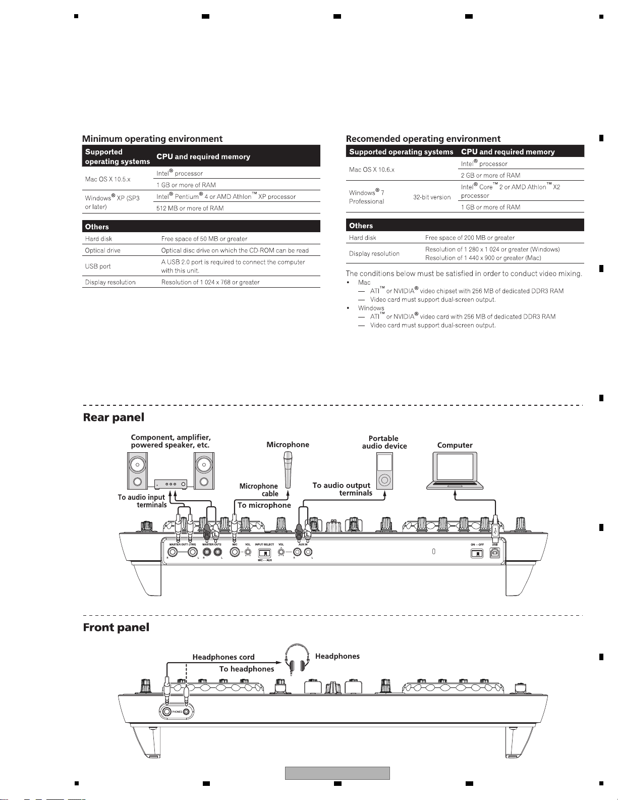
5
[Preparations]
[Connection]
Install VIRTUAL DJ LE (DJ software) on the PC. For details on installation, refer to the operation manual of the unit.
If the OS of the PC is Windows, the driver software for outputting audio from the PC must be installed beforehand.
The requirements of a PC on which VIRTUAL DJ LE can be installed are as shown below.
6 7 8
5.5 OPERATION CHECK METHODS, USING VIRTUAL DJ
A
B
C
D
E
F
DDJ-ERGO-V
5
6 7 8
27
Page 28

1
[Startup of the System]
• Starting up the DDJ-ERGO-V
1. Connect this unit and a PC, using a USB cable.
2. Start up the connected PC.
3. Slide the ON/OFF switch of this unit to ON to turn it on.
4. Turn on the connected microphone(s) and external equipment.
[Loading and Playing a Track]
1. While holding the SHIFT button pressed, turn the rotary selector to select a folder or an item.
2. After releasing the SHIFT button, turn the rotary selector to select a track.
3. Press the LOAD button to load the selected track onto the deck.
4. Play the track by pressing the [f] button.
[Outputting Audio]
1. Adjust the level of the audio signal output from each deck, using the GAIN control and the channel fader.
For switching the decks from which the audio signal is output, use the cross fader.
2. Adjust the audio level from the speakers, using the MASTER VOL control, in order to confirm that the audio signal is output
without a problem. The MASTER VOL and HEADPHONE VOL controls on the controller are not interlocked with the
GUI VOL controls for VIRTUAL DJ LE.
If no sound is output even if you turn the above-mentioned controls on the controller, check if the GUI VOL controls for
VIRTUAL DJ LE are set to MIN.
Select a deck to be monitored via the headphones using the HEADPHONE [CUE] button and adjust the audio level, using
the HEADPHONE [VOL] control, in order to confirm that the audio signal is output without a problem.
[Inputting Audio]
Example: When inputting audio from external equipment
1. Connect the external equipment via the AUX IN connector then set the AUX/MIC selector to AUX.
2. Adjust the input audio level, turning the AUX IN VOL control on the rear panel. Adjust the output audio level, turning the
AUX/MIC VOL control on the upper right of the control panel, then check that the audio signal is output properly.
* The details see operating instructions.
• Starting up VIRTUAL DJ LE
(Windows)
1. From the Start menu of the Windows, select All Programs, VIRTUAL DJ LE, then VirtualDJ LE(DDJ-ERGO).
When VIRTUAL DJ LE is started for the first time, the serial number input window will be displayed.
Enter the serial number for servicing for VIRTUAL DJ LE, which is posted on the Niis Web site, then click on OK.
2. After the VIRTUAL DJ LE window is displayed, click on CONFIG located in the upper right portion of the window.
The Settings window is displayed. Select the Sound Setup tab and set the following items in the order described below.
1 [Inputs]: Select MICROPHONE.
2 [Sound card]: Select Pioneer DDJ ASIO. Check the "Ultra-latency".
3 [Outputs]: Select [Master: Chan 1&2/Headphones: Chan 3&4].
3. Click on Apply then OK.
(Macintosh)
1. With the Finder, open the Applications folder then double-click on the VIRTUAL DJ LE icon.
(Enter the serial number in the same way as that for Windows.)
2. After the VIRTUAL DJ LE is displayed, click on CONFIG located in the upper left portion of the window.
The Settings window is displayed. Select the Sound Setup tab and set the following items in the order described below.
1 [Inputs]: Select MICROPHONE.
2 [Sound card]: Select [4-IN/4-OUT CARD] and [PIONER DDJ-ERGO]. Check the "Ultra-latency".
3 [Outputs]: Select [Master: Chan 1&2/Headphones: Chan 3&4].
3. Click on Apply then OK.
A
2 3 4
B
C
D
E
F
28
1
2 3 4
DDJ-ERGO-V
Page 29
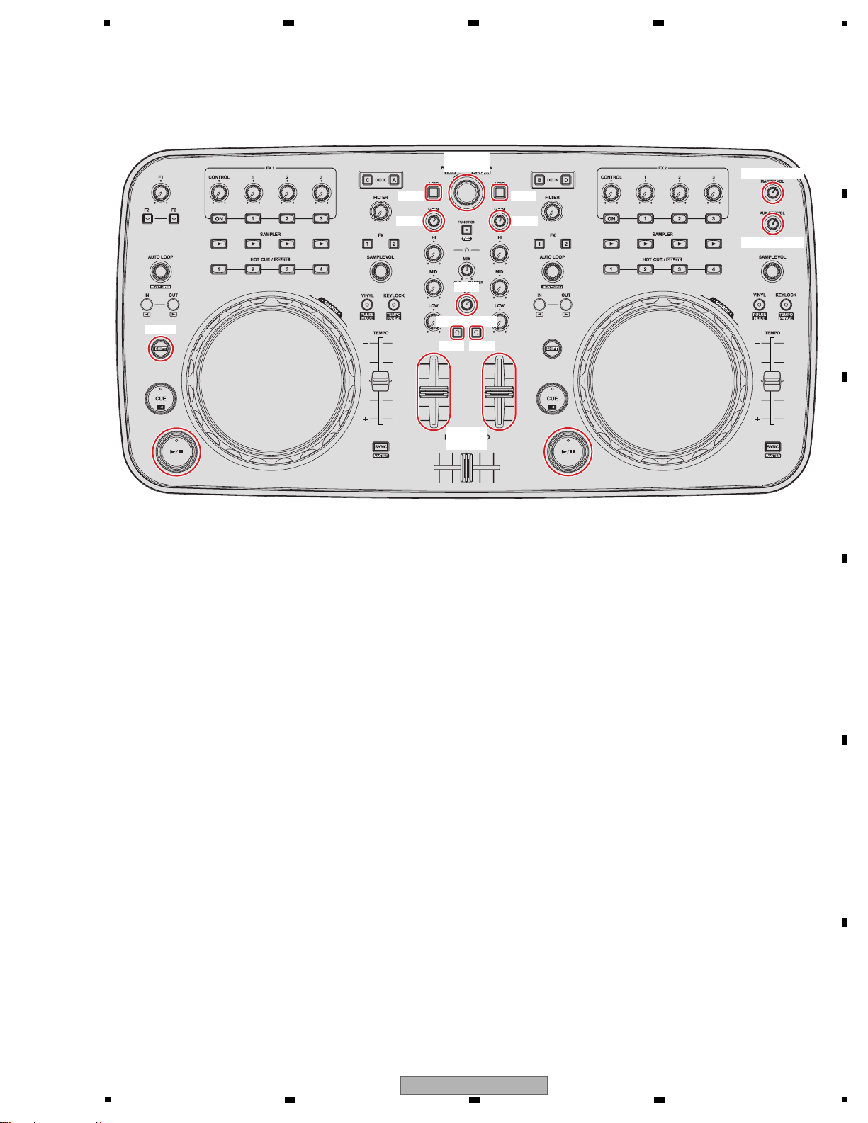
5
MASTER VOL
AUX/MIC VOL
GAIN
HEADPHONE
VOL
CUE CUE
LOADLOAD
GAIN
Rotary
selector
SHIFT
Channel
fader
[Operation elements to use at the operation check]
6 7 8
A
B
C
D
E
F
DDJ-ERGO-V
5
6 7 8
29
Page 30
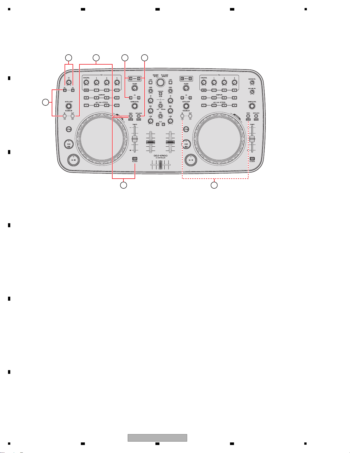
1
How to start up and enter various modes in a manner other than the usual is described below.
1 Program for USB Controller copy mode
While simultaneously holding the LOOP OUT and VINYL buttons on the Deck A/C side pressed, set the Power switch of the unit to ON.
Data for the TUSB firmware in the MAIN_UCOM will be copied to the EEPROM.
During copying, the FUNCTION LED is lit.
For details, see “8.2 HOW TO PROGRAM COPY FOR USB CONTROLLER.”
3 Version of the firmware Confirmation mode (with hardware alone)
While simultaneously holding the DECK A and KEYLOCK buttons on the Deck A/C side pressed, set the Power switch of the unit to ON.
The version number will be indicated with the LEDs on the controller, with no need for starting up any application.
For details, see “6.2 FIRMWARE VERSION CONFIRMATION METHODS.”
4 Service mode
While simultaneously holding the LOOP IN and F2 buttons on the Deck A/C side pressed, set the Power switch of the unit to ON.
In this mode, you can check if each element on the controller can operate and each LED can light properly, with no need for starting up
any application.
For details, see “6.3 SERVICE MODE.”
5 JOG Load Measurement mode
While simultaneously holding the F2 and F3 buttons on the Deck A/C side pressed, set the Power switch of the unit to ON.
This mode is for judging if the load value for the JOG dial while it is being turned is OK.
For details, see “8.4 JOG DIAL ROTATION LOAD ADJUSTMENT.”
6 Point-of-Sale Demo mode
Demonstrations with lighting of the LEDs (illumination) are automatically performed at shops even if no PC application is started.
This mode will be established if no reception via MIDI is performed for 1 minute after the controller is turned ON.
7 Factory Reset (To return the settings to the factory default values)
While simultaneously holding the DECK C and FX 1 buttons on the Deck A/C side pressed, set the Power switch of the unit to ON.
The VINYL mode ON/OFF and Normal/Active mode are reset to the initial settings.
For details, see “6.4 FACTORY RESET MODE.”
2 Firmware update
Set the Power switch to ON without pressing any other buttons.
Data for all areas in the ROM, excluding those for the boot area, will be rewritten.
For details, see “8.3 HOW TO FIRMWARE UPDATE.”
15
2 2
37
4
2 3 4
6. SERVICE MODE
6.1 HOW TO ENTER EACH MODE
A
B
C
D
E
F
30
1
2 3 4
DDJ-ERGO-V
Page 31

5
1. Click on Start then select Programs, Pioneer, DDJ, then DDJ Version Display Utility, to start up the utility.
• This method can be used only with Windows, and with Mac OS the firmware version cannot be confirmed in this way.
• The firmware version can be confirmed only on a PC on which the dedicated driver for the DDJ-ERGO has been installed.
2. Check the version described in the Firmware section.
How to Confirm the Firmware Version on the Connected PC
6 7 8
6.2 FIRMWARE VERSION CONFIRMATION METHODS
A
B
C
D
E
F
DDJ-ERGO-V
5
6 7 8
31
Page 32

1
Confirming the Firmware Version (MAIN_UCOM) and Confirming the Mode setting
(VINYL mode and jog dials' illumination mode)
1 Integral part of the version number
(LEDs on DECK A lit)
[Numerics expressed with the number of lit LEDs]
To enter this mode, while simultaneously holding the DECK A and KEYLOCK buttons on the Deck A/C side pressed, set the
Power switch of the unit to ON.
(Hold the two buttons pressed until the opening display terminates.)
The version number of the firmware (MAIN_UCOM) will be indicated with LED-lighting patterns that are switched every
3 seconds in integral part and decimal fraction part.
In the blocks that are indicated with the red frames in the figures, the number of lit LEDs indicates the corresponding number.
In addition to the above-mentioned firmware-version indication, the setting statuses of VINYL mode and Illumination mode
for the Jog dial are indicated with other LEDs.
* For details, see “6.4 FACTORY RESET MODE.”
x . xx
2 Decimal fraction part of the version number
(LEDs on DECKs A and B lit)
x . xx
01234
56789
3 sec
Mode Point Mode setting state LED display
VINYL mode
DECK A/C
DECK B/D
ON
VINYL LED on the DECK A/C side lit
OFF
VINYL LED on the DECK A/C side unlit
ON
VINYL LED on the DECK B/D side lit
OFF
VINYL LED on the DECK B/D side unlit
Illumination mode
JOG dial
Pulse Mode: Active
Blue LEDs on both decks lit
Pulse Mode: Normal
Blue LEDs on both decks unlit
A
2 3 4
B
C
D
E
F
32
1
DDJ-ERGO-V
2 3 4
Page 33

5
Confirmation of Input to Each Element and Display Function
To enter this mode, while holding the LOOP IN and F2 buttons on the Deck A/C side pressed, set the Power switch to ON.
(Hold the two buttons pressed until the opening display terminates.)
In this mode, you can check if pressing each of button or turning of the JOG dial is properly input and indications are also properly displayed.
The indication corresponding to a pressed button is lit only while the button is held pressed.
Part Operator Device LED Display Deck
DECK A BUTTON DECK A 1
DECK C BUTTON DECK C 1
DECK B BUTTON DECK B 2
DECK D BUTTON DECK D 2
FX1 EFFECT ON/OFF BUTTON EFFECT ON 1
EFFECT CONTROL ROTARY VOLUME JOG LED ROTATION A1
EFFECT PARAMETER 1 ON/OFF
BUTTON EFFECT PARAMETER 1 1
EFFECT PARAMETER 2 ON/OFF
BUTTON EFFECT PARAMETER 2 1
EFFECT PARAMETER 3 ON/OFF
BUTTON EFFECT PARAMETER 3 1
EFFECT PARAMETER 1 CONTROL
ROTAR Y VOLUME JOG LED ROTATION A1
EFFECT PARAMETER 2 CONTROL
ROTAR Y VOLUME JOG LED ROTATION A1
EFFECT PARAMETER 3 CONTROL
ROTAR Y VOLUME JOG LED ROTATION A1
FX2 EFFECT ON/OFF BUTTON EFFECT ON 2
EFFECT CONTROL ROTARY VOLUME JOG LED ROTATION B2
EFFECT PARAMETER 1 ON/OFF
BUTTON EFFECT PARAMETER 1 2
EFFECT PARAMETER 2 ON/OFF
BUTTON EFFECT PARAMETER 2 2
EFFECT PARAMETER 3 ON/OFF
BUTTON EFFECT PARAMETER 3 2
EFFECT PARAMETER 1 CONTROL
ROTAR Y VOLUME JOG LED ROTATION B2
EFFECT PARAMETER 2 CONTROL
ROTAR Y VOLUME JOG LED ROTATION B2
EFFECT PARAMETER 3 CONTROL
ROTAR Y VOLUME JOG LED ROTATION B2
DECK A/C FILTER CONTROL ROTARY VOLUME JOG LED ROTATION A1
LOOP IN BUTTON LOOP IN 1
LOOP OUT BUTTON LOOP OUT 1
AUTO LOOP ENCODER JOG LED ROTATION A1
AUTO LOOP PUSH ENCODER LOOP IN 1
VINYL BUTTONVINYL 1
SYNC A/C BUTTON SYNC A/C 1
HOT CUE 1 BUTTON HOT CUE 1 1
HOT CUE 2 BUTTON HOT CUE 2 1
HOT CUE 3 BUTTON HOT CUE 3 1
HOT CUE 4 BUTTON HOT CUE 4 1
SAMPLER 1 BUTTON SAMPLER 1 1
SAMPLER 2 BUTTON SAMPLER 2 1
SAMPLER 3 BUTTON SAMPLER 3 1
SAMPLER 4 BUTTON SAMPLER 4 1
SAMPLER VOL ENCODER JOG LED ROTATION A1
SAMPLER VOL PUSH ENCODER VINYL 1
SHIFT BUTTON LOOP OUT 1
KEY LOCK BUTTON KEY LOCK 1
CUE BUTTON CUE 1
PLAY/PAUSE BUTTON PLAY/PAUSE 1
TEMPO SLIDE VOLUME JOG LED ROTATION A1
JOG R
O
TATION DIAL JOG LED ROTATION A1
JOG TOUCH DIAL JOG LED ALL ON 1
6 7 8
6.3 SERVICE MODE
A
B
C
D
E
F
DDJ-ERGO-V
5
6 7 8
33
Page 34

1
Part Operator Device LED Display Deck
DECK B/D FILTER CONTROL ROTARY VOLUME JOG LED ROTATION B2
LOOP IN BUTTON LOOP IN 2
LOOP OUT BUTTON LOOP OUT 2
AUTO LOOP ENCODER JOG LED ROTATION B2
AUTO LOOP PUSH ENCODER LOOP IN 2
VINYL BUTTONVINYL 2
SYNC B/D BUTTON SYNC B/D 2
HOT CUE 1 BUTTON HOT CUE 1 2
HOT CUE 2 BUTTON HOT CUE 2 2
HOT CUE 3 BUTTON HOT CUE 3 2
HOT CUE 4 BUTTON HOT CUE 4 2
SAMPLER 1 BUTTON SAMPLER 1 2
SAMPLER 2 BUTTON SAMPLER 2 2
SAMPLER 3 BUTTON SAMPLER 3 2
SAMPLER 4 BUTTON SAMPLER 4 2
SAMPLER VOL ENCODER JOG LED ROTATION B2
SAMPLER VOL PUSH ENCODER VINYL 2
SHIFT BUTTON LOOP OUT 2
KEY LOCK BUTTON KEY LOCK 2
CUE BUTTON CUE 2
PLAY/PAUSE BUTTON PLAY/PAUSE 2
TEMPO SLIDE VOLUME JOG LED ROTATION B2
JOG ROTATION DIAL
JOG LED R
OTATION B2
JOG TOUCH DIAL JOG LED ALL ON 2
MIXER LOAD A/C BUTTON FX 1 A/C 1
LOAD B/D BUTTON FX 1 B/D 2
FUNCTION BUTTON FUNCTION 1/2
BROWSE CONTROL ENCODER JOG LED ROTATION A/B 1/2
BROWSE PUSH ENCODER ALL LED BRIGHT → OFF → (Cyclic) 1/2
GAIN CONTROL A/C ROTARY VOLUME JOG LED ROTATION A1
GAIN CONTROL B/D ROTARY VOLUME JOG LED ROTATION B2
EQ HI A/C ROTARY VOLUME JOG LED ROTATION A1
EQ HI B/D ROTARY VOLUME JOG LED ROTATION B2
EQ MID A/C ROTARY VOLUME JOG LED ROTATION A1
EQ MID B/D ROTARY VOLUME JOG LED ROTATION B2
EQ LOW A/C ROTARY VOLUME JOG LED ROTATION A1
EQ LOW B/D ROTARY VOLUME JOG LED ROTATION B2
MASTER VOL ROTARY VOLUME JOG LED ROTATION A/B 1/2
HEADPHONE MIX
R
OTARY VOLUME JOG LED ROTATION A/B 1/2
HEADPHONE VOL ROTARY VOLUME JOG LED ROTATION A/B 1/2
AUX/MIC VOL ROTARY VOLUME JOG LED ROTATION A/B 1/2
F1 ROTARY VOLUME JOG LED ROTATION A/B 1/2
F2 BUTTON F2 1/2
F3 BUTTON F3 1/2
FX 1 A/C BUTTON FX 1 A/C 1
FX 1 B/D BUTTON FX 1 B/D 2
FX 2 A/C BUTTON FX 2 A/C 1
FX 2 B/D BUTTON FX 2 B/D 2
HEADPHONE CUE A/C BUTTON HEADPHONE CUE A/C 1
HEADPHONE CUE B/D BUTTON HEADPHONE CUE B/D 2
FADER A/C SLIDE VOLUME JOG LED ROTATION A1
FADER B/D SLIDE VOLUME JOG LED ROTATION B2
CROSS FADER SLIDE VOLUME JOG LED ROTATION A/B 1/2
A
2 3 4
B
C
D
E
F
34
DDJ-ERGO-V
1
2 3 4
Page 35

5
[Indications by the VOL control]
The volume level is indicated in 16 steps from minimum to maximum.
At the minimum volume, LEDs 17, 18, and 19 are lit, with LED 18 brighter than other two. The lighting LEDs shift as the volume
is increased, and LEDs 8, 9, and 10 are lit at the maximum volume.
[Indications by the FADER control]
The fader level is indicated in 16 steps from minimum to maximum.
At the minimum level, LEDs 24, 1, and 2 are lit, with LED 1 brighter than other two. The lighting LEDs shift as the level is
increased, and LEDs 15, 16, and 17 are lit at the maximum level.
MIN MAX
MIN MAX
1
24
2
3
4
5
6
7
8
9
10
11
12
13
23
22
21
20
19
18
17
16
15
14
25
2627
28
1
24
2
3
4
5
6
7
8
9
10
11
12
13
23
22
21
20
19
18
17
16
15
14
25
2627
28
1
24
2
3
4
5
6
7
8
9
10
11
12
13
23
22
21
20
19
18
17
16
15
14
25
2627
28
1
24
2
3
4
5
6
7
8
9
10
11
12
13
23
22
21
20
19
18
17
16
15
14
25
2627
28
6 7 8
A
B
C
D
E
5
DDJ-ERGO-V
6 7 8
F
35
Page 36

1
OK NG
To enter this mode, while simultaneously holding the DECK C and FX 1 buttons on the Deck A/C side pressed, set the Power
switch of the unit to ON.
(Hold the two buttons pressed until the opening display terminates.)
During Factory Reset mode, the VINYL LEDs on both sides are lit. When you exit this mode, the LEDs go dark.
1) Checking VINYL ON/OFF
After the unit is turned on and the opening illumination is finished, if the VINYL LED is lit, it is set to ON (OK).
2) Checking of Normal/Active Mode
Check the following, after starting the application on the connected PC.
Load a piece of music onto any of the decks (Deck A, B, C, or D).
Check that blue LEDs on the JOG dial are lit (Active mode).
1) Checking VINYL ON/OFF
Check the same as described in 1) of a).
2) Checking of Normal/Active Mode
Check that blue LEDs on the JOG dial are lit (Active mode).
(LED indication is the same as described in 2) of a).
OK NG
a) Checking Method with an Application on the Connected PC
Establish Version Confirmation mode, by turning the unit ON while simultaneously holding the DECK A and KEYLOCK
buttons on the A/C deck side pressed.
a) Checking Method With the Controller Alone
1. Initial Settings
2. How to Check If Initial Settings Are Restored
VINYL on the left deck
VINYL on the right deck
Normal / Active mode
ON
ON
Active
2 3 4
6.4 FACTORY RESET MODE
A
B
C
D
E
F
36
1
2 3 4
DDJ-ERGO-V
Page 37

5
If a drop in voltage for VBUS power is detected, a power-saving mode will be automatically established, limiting the
headphones maximum output level.
Two types of power-saving mode are provided, as shown below.
Mode State Note
1 Power-Saving mode 1
(when a voltage drop to
4.2–4.5 V is detected)
Headphones maximum output: To be
decreased from the normal level
The DECK LED flashes at cycle of 1 sec.
If normal voltage is recovered, the headphones output level
and the DECK LED will return to normal states.
2 Power-Saving mode 2
(when a voltage drop
further down than in
Power-Saving mode 1
[4.2 V or less ] is detected)
Headphones maximum output: To be
decreased further than in mode 1
The TUSB microcomputer will be reset and
restart.
The DECK LED flashes at cycle of 0.5 sec.
If the voltage is not restored even after the TUSB
microcomputer is reset and restart, DECK LED will flash at
cycle of 0.2 sec.
All operations will be disabled.
When abnormalities are detected during the time of carrying out power supply ON, or operation, it displays by LED.
Abnormalities LED/Display Note
1 Abnormalities of a power
supply
Left deck/CH Fader
blinks
When abnormalities are detected by the state of DC power supply and
USB bus power supply, it will be in this state. Opening display is not
performed, either, when abnormalities are detected at the time of starting.
2 Abnormalities in
FLASH-ROM of
MAIN_UCOM
Left deck/LOOP-IN
Lighting
When update goes wrong and FLASH-ROM is not written correctly, it
will be in this state. Even in this case, update can be performed
succeedingly. However, "3" is displayed while it can be communicating
neither with the case where USB cable is not connected, nor USB
controller, correctly also at this time.
3 Aabnormalities of
USB controller
Left deck/LOOP-OUT
Blinks in a cycle of 1 seconds.
When the time when it cannot communicate with USB controller correctly
although USB cable is connected at the time of starting, and controllers
are abnormalities, it will be in this state.
4 EEPROM writing error FUNCTION
Blinks in a cycle of 1 seconds.
Become this state at an EEPROM writing error.
Device Name Function Part No. Reference No. Assy
MAIN UCOM Main control, all function / LED control PEQ033A8 IC1002 CDJ1 Assy
USB Controller USB control, Audio control TUSB3200A IC102 IFPW Assy
6.5 POWER-SAVING MODE
6 7 8
A
B
6.6 ERROR DISPLAY
6.7 ABOUT THE DEVICE
C
D
E
F
DDJ-ERGO-V
5
6 7 8
37
Page 38

1
C
Dial Knob S (B)
(DAA1273) ×4
Black
White
A
Dial Knob
(DAA1259) ×1
Black Black
E
Knob/SLD
(DNK6008) ×2
F
Slider Knob 1
(DAC2684) ×3
Slider Knob 1
Slider Knob 2
Stopper/SLD
Slider Knob 2
(DAC2685) ×3
Stopper/SLD
(DNK6009) ×3
White
White
Black
D
Knob/LBK
(DAA1284) ×17
White
Black
White
Black
B
Rotary Knob S (Black)
(DAA1262) ×6
ADD DD D
C
C
B B
C
C
D
D
E EF
Note: Even if the unit shown in the photos and illustrations in this manual may differ from your product, the
procedures described here are common.
Knobs and Volumes Location
2 3 4
7. DISASSEMBLY
A
B
C
D
E
F
38
DDJ-ERGO-V
1
2 3 4
Page 39

5
[1] Chassis Section
(1) Reverse the product.
(2) Remove the 10 screws. (BPZ30P080FNI)
(3) Remove the two screws. (PBZ30P080FTC)
(4) Remove the chassis section.
Chassis section
Control panel section
• Bottom view
2
×10
3
4
×2
Diagnosis
Disassembly
6 7 8
A
B
C
D
E
F
DDJ-ERGO-V
5
6 7 8
39
Page 40

1
[2] HPJK, HPLC, JACK and IFPW Assemblies
• HPJK Assy
(1) Disconnect the one connector.
(2) Remove the two screws, and remove the
stopper/HP. (BPZ30P080FNI)
(3) Remove the two screws, and remove the
HPJK Assy with stay/HP. (BPZ30P080FNI)
(4) Remove the one nut, one screw and remove
the HPJK Assy. (BBZ30P060FTC)
• JACK, IFPW Assy
(1) Remove the two screws. (PMB30P080FTB)
(2) Remove the one screw and remove the
stay/PCB with Assy. (BPZ30P080FNI)
(3) Remove the three nuts.
(4) Remove the two screws. (BBZ30P060FTC)
(5) Remove the two screws. (BPZ30P080FNI)
(6) Remove the one screw. (DBA1340)
(7) Remove the seven screws and remove the
JACK and IFPW Assemblies.
(BBZ30P060FTC)
• HPLC Assy
(5) Disconnect the one connector.
(6) Remove the two screws, and remove the
HLD3 Assy. (BPZ30P080FNI)
(7) Remove the HPLC Assy.
Stopper/HP
Stay/HP
CN103
CN104
HPJK Assy
HPJK Assy
HLD3 Assy
JACK Assy
IFPW Assy
HPLC Assy
Stay/PCB
Stay/PCB
2
×2
3
×3
4
4
5
5
1
1
6
6
7
×2
3
4
2
4
1
×2
5
A
A B
B
C D
Screw tightening order
Screw tightening order
7
×4
7
×3
A
2 3 4
B
C
D
E
F
40
1
2 3 4
DDJ-ERGO-V
Page 41

5
[3] CDJ1, CDJ2, CRFD Assemblies and JOG Section
[3-1] Knobs and VRs
(1) Remove the all knobs.
Note: When you remove the knob of the A part,
pull it up to a course directly overhead
necessarily.
(2) Remove the three silider knobs 2,
three slider knobs 1, three stopper/SLD.
(See below.)
1
×30
2
×3
1 Find the side on which the line reaches
the bottom.
4 Remove the slider knob 1.
3 Remove the slider knob 2.2 Insert a pair of tweezers etc. beneath
the line then push the slider knob 2
upward. To protect the panel from being
scratched, use protective material.
• Disassembly of the slider knob
The reference of the direction
The new slider knob adopted by this product is designed so that it is not pulled out easily.
Therefore, the method for removing the slider knob is different from the conventional method; it can only be pulled out after
slider knob 2 is removed.
Protective materialTweezers
Slider knob 2
Slider knob 1
Slider knob 2
*: During reassembly, fully push
down Slider knob 2 until it is
dented into Slider knob 1.
5 Remove the stopper/SLD.
Stopper/SLD
Side on which
the line reaches the bottom
Stopper
(right direction)
Stopper
(rear direction)
A A
6 7 8
A
B
C
D
5
DDJ-ERGO-V
6 7 8
E
F
41
Page 42

1
• Bottom view
[3-2] CDJ1, CDJ2, CRFD Assemblies and JOG section
(1) Reverse the control panel section.
(2) Disconnect the four connectors.
(3) Remove the 11 screws and remove the
barrier 1 and barrier 2. (BPZ30P080FNI)
(4) Remove the eight screws. (BPZ30P100FTB)
(5) Remove the one screw and remove the cord
clamper. (BPZ30P080FNI)
(6) Remove the 36 screws and remove the
CDJ1, CDJ2 and CRFD Assemblies.
(BPZ30P080FNI)
(7) Remove the two JOG section.
[3-3] Stay/VR
(1) Remove the 10 nuts and 10 washers.
(2) Remove the two screws. (IMZ30P040FTC)
(3) Remove the four screws. (PMH20P040FTC)
(4) Remove the stay/VR.
Barrier/2
Barrier/1
CDJ1 Assy
CDJ1 Assy
JOG section
Stay/VR
3
×5
4
×4
3
×4
2
×2
4
7
7
6
5
×4
3
×6
6
×14
6
×21
1
×10
CN2002
CN1002
CN2801
2
2
2
2
CN1801
4
CDJ2 Assy
CRFD Assy
Barrier/1Barrier/2
A
A
A
B
A
Screw tightening order
The other screws are random order.
Screw tightening order
The other screws are random order.
JOG section
A
B
2 3 4
C
D
E
F
42
1
DDJ-ERGO-V
2 3 4
Page 43

5
Perform the corresponding task(s) in the described order after any of the following parts is replaced:
After repairing, be sure to check the version of the firmware, and if it is not the latest one,
update to the latest version.
In addition, be sure to reset the unit to the default settings, using Factory Reset mode, before
returning the repaired product to the user.
• MAIN UCOM (CDJ1 Assy: IC1002)
• Confirmation of the version of the firmware
• Updating to the latest version of the firmware
• EEPROM (IFPW Assy: IC104)
• Copying the program for the USB controller
• Updating to the latest version of the firmware
• Copying the program for the USB controller
• Component parts of the JOG dial section • JOG dial rotation load adjustment
1. Check that the controller is OFF.
2. While holding the LOOP OUT 1 and VINYL 1 buttons pressed, set the Power switch of the unit to ON.
Note: NEVER release the above-mentioned two buttons while the FUNCTION LED is lit.
3. After making sure that the FUNCTION LED is unlit, set the Power switch of the unit to OFF.
LOOP OUT 1 button : S1227
VINYL 1 button : S1208
FUNCTION LED : D1203
Note: If copying fails, the FUNCTION LED will flash at intervals of 0.25 sec.
6 7 8
8. EACH SETTING AND ADJUSTMENT
8.1 NECESSARY ITEMS TO BE NOTED
A
B
8.2 HOW TO PROGRAM COPY FOR USB CONTROLLER
C
D
E
F
DDJ-ERGO-V
5
6 7 8
43
Page 44

1
Starting/Selection of a language
(English is chosen.)
Check of a version
(Click a [START])
End.
(Click a [OK])
Controller is re-started automatically.
The device which update a firmware is MAIN UCOM.
USB connection of the controller is made at PC/MAC, and it updates by performing the update program of exclusive use.
Download the zipped updater file for the latest firmware from Niis then execute the unzipped file on the PC.
The filenames for the updater are shown below.
Fielname Filename after the thawing
Windows: DDJ-ERGOvXXX.zip Windows: DDJ-ERGOUpdater_verXXX.exe
Mac: DDJ-ERGOvXXX.dmg Mac: DDJ-ERGOUpdater_verXXX.app
Note: xxx is version number. If it is Ver1.00, it is DDJERGOv_100.zip/DDJERGOv_100.dmg.
CAUTION: When you update, please terminate all DJ applications, such as VIRTUAL DJ.
2 3 4
8.3 HOW TO FIRMWARE UPDATE
A
B
C
D
E
F
44
1
2 3 4
DDJ-ERGO-V
Page 45

5
1. How to Enter JOG Load Measurement Mode
2. How to Measure
To enter this mode, while holding the F2 and F3 buttons on the Deck A/C side pressed, set the Power switch to ON.
During this mode, the KEYLOCK LEDs on both sides are lit.
(Hold the two buttons pressed until the opening display terminates.)
The load (light or heavy) on the JOG dial when it is turned can be objectively judged in this mode.
When the JOG dial is rotated swiftly in this mode, the maximum speed and time required for slowdown, as defined below, are
measured. When the maximum speed reaches 7 times normal speed or higher, time required for slowdown is calculated then
evaluated as to whether or not it is within the specified range, then the result will be indicated by the LEDs.
Either rotation direction, clockwise or counterclockwise, is okay.
Maximum speed: Maximum speed with normal speed defined as when one rotation takes 1.8 sec
Time required for slowdown: Time required for the rotation speed to slow down from 3 times to 1.5 times normal speed
To measure the time required for slowdown, the maximum speed must be 7 times normal speed or higher.
If the maximum speed does not reach 7.0 times normal speed, the JOG LEDs flash three times as a warning.
The number of measurements up to the fourth time is indicated by the LEDs.
First measurement finished: HOT CUE 1 lit
Second measurement finished: HOT CUE 2 lit
Third measurement finished: HOT CUE 3 lit
Fourth measurement finished: HOT CUE 4 lit
3. Judgment
After four measurements of time required for slowdown are finished, the mean value of the four measurement results is
calculated and judged as to whether or not it is within the specified range. The result will be indicated with the LEDs.
The specified range is 100 ± 40 msec.
OK: VINYL lit
NG (lighter): LOOP OUT lit
NG (heavier): LOOP IN lit
The 5th time or subsequent measurement can be performed, but the number of times of measurement is not indicated with
the LEDs. The mean value of the results of all the measurements is calculated, and its result will be indicated with the LEDs.
Adjust plate
Fig. 1
6 7 8
8.4 JOG DIAL ROTATION LOAD ADJUSTMENT
A
B
C
D
E
F
DDJ-ERGO-V
5
6 7 8
45
Page 46

1
NOTES: - Parts marked by “NSP” are generally unavailable because they are not in our Master Spare Parts List.
-
The > mark found on some component parts indicates the importance of the safety factor of the part.
Therefore, when replacing, be sure to use parts of identical designation.
-
Screws adjacent to b mark on product are used for disassembly.
-
For the applying amount of lubricants or glue, follow the instructions in this manual.
(In the case of no amount instructions, apply as you think it appropriate.)
Front
2 3 4
9. EXPLODED VIEWS AND PARTS LIST
A
9.1 PACKING SECTION
B
C
D
E
F
46
1
2 3 4
DDJ-ERGO-V
Page 47

5
PACKING SECTION PARTS LIST
Mark No. Description Part No.
1 USB Cable DDE1128
2 VIRTUAL DJ LE DXX2685
software CD-ROM
3Driver software/ DRU1001
operating instructions CD-ROM
4 Read Before Use (Important) DRH1122
5Quick Start Guide DRH1123
6Hardware Diagram for Virtual DJDRH1124
(Table of Supported Functions)
NSP 7 License Key Label Assy DXA2251
6 7 8
A
NSP 8 Warranty Card DRY1259
NSP 9 Warranty Card ARY7043
NSP 10 Warranty Card ARY7107
NSP 11 Service network list ARY1127
(for Japanese customers)
NSP 12 Label/L K DRW2484
NSP 13 Vinyl Bag AHG7031
NSP 14 Polyethylene Bag AHG7117
15 Pad/A DHA1878
16 Pad/B DHA1879
17 Pad/ACC DHA1880
18 Packing Case/V DHG3079
19 Sheet RHX1006
20 Plastic Handle (PE) VEC2292
21 Spacer (PE) VEC2293
B
C
D
E
F
DDJ-ERGO-V
5
6 7 8
47
Page 48

1
CONTACT SIDE
NON-CONTACT
SIDE
A
A
B
C
C
B
A
B
C
E
Refer to
"9.3 CONTROL PANEL SECTION".
9.2 EXTERIOR SECION
A
B
2 3 4
C
D
E
F
48
DDJ-ERGO-V
1
2 3 4
Page 49

5
6 7 8
EXTERIOR SECION SECTION PARTS LIST
Mark No. Description Part No.
1 JACK Assy DWX3304
2 HPJK Assy DWX3306
3 HLD3 Assy DWX3311
4 HPLC Assy DWX3324
5 IFPW Assy DWX3301
6 FFC/27P DDD1585
7Rubber Foot (H6) DEB1996
8 Stay/PCB DNH3000
9 Stay/HP DNH3002
10 Stopper/HP DNH3006
A
11 Chassis DNK6005
12 Rubber Foot VEB1349
13 Dial Knob DAA1259
14 Rotary Knob S (Black) DAA1262
15 Dial Knob S (B) DAA1273
16 Knob/LBK DAA1284
17 Slider Knob 1 DAC2684
18 Slider Knob 2 DAC2685
19 Rear Panel/V DAH2864
NSP 20 Cushion/A DEC3402
NSP 21 Cushion/B DEC3403
22 Foot/R DNK6006
23 Foot/L DNK6007
24 Knob/SLD DNK6008
25 Stopper/SLD DNK6009
NSP 26 Label/V DRW2492
27 • • • • •
28 • • • • •
29 Nut (M12) NKX2FNI
30 Screw BBZ30P060FTC
B
C
D
31 Screw BPZ30P080FNI
32 Screw (M3x5) DBA1340
33 Screw PBZ30P080FTC
34 Screw PMB30P080FTB
5
6 7 8
DDJ-ERGO-V
E
F
49
Page 50

1
B
D
A
C
D
G
F
• Bottom view
D
C
B
A
CONTACT SIDE
NON-CONTACT
SIDE
Refer to
"9.4 JOG SECTION".
Washer (Accessories of VR)
Nut (Accessories of VR)
Refer to
"9.4 JOG SECTION".
9.3 CONTROL PANEL SECTION
A
B
2 3 4
C
D
E
F
50
DDJ-ERGO-V
1
2 3 4
Page 51

5
CONTROL PANEL SECTION PARTS LIST
Mark No. Description Part No.
1 CDJ1 Assy DWX3302
2 CDJ2 Assy DWX3303
3 CRFD Assy DWX3305
4 FFC/39P DDD1586
5 FFC/39P DDD1587
6 Stay/VR DNH3005
7Button S (Black) DAC2663
8Button/LOP DAC2783
9Button/1 DAC2785
10 Button/SNC DAC2791
6 7 8
A
11 Button/2 DAC2792
12 Button/3 DAC2793
13 Button/4 DAC2794
14 Button/FNC DAC2795
15 Button/FX DAC2796
16 Button/CUE DAC2797
17 Button/A DAC2798
18 Button/B DAC2799
19 Button/C DAC2800
20 Button/D DAC2801
21 Button/PRV DAC2802
22 Button/VNL DAC2806
23 Fader Packing DEC3355
24 Packing/TMP DEC3392
25 Barrier/1 DEC3393
26 Barrier/2 DEC3394
27 Lens/FDR DNK5989
28 Control Panel DNK6000
29 Play Button Assy DXA2252
30 Cord Clamper (Steel) RNH-184
B
C
D
31 • • • • •
32 • • • • •
33 Screw BPZ30P080FNI
34 Screw BPZ30P100FTB
35 Screw IMZ30P040FTC
36 Screw PMH20P040FTC
5
6 7 8
DDJ-ERGO-V
E
F
51
Page 52

1
Bottom view
H I
J K
Lubricating oil
(GYA1001)
Lubricating oil
(GYA1001)
Arm spring
Encoder arm
Hook
Hook
CDJ1 CN1002
or
CDJ2 CN2002
CDJ1 JH1001
or
CDJ2 JH2001
or
or
or
9.4 JOG SECTION
A
B
2 3 4
C
D
E
F
52
1
2 3 4
DDJ-ERGO-V
Page 53

5
JOG SECTION PARTS LIST
Mark No. Description Part No.
1 JOG1 Assy DWS1436
2 JOG2 Assy DWS1438
3 TCH1 Assy DWS1437
4 TCH2 Assy DWS1439
5 HLD1 Assy DWX3309
6 HLD2 Assy DWX3310
7 Plate/JOG DAH2862
8 Arm Spring DBH1612
9Lever Spring DBH1626
10 Load Spring DBH1676
6 7 8
A
11 Encoder Plate DEC2889
12 Lever Cushion (A) DEC3001
13 Lever Cushion (B) DEC3002
14 JOG Lever DNK4763
15 JOG Shaft DNK4934
16 Encoder Arm DNK4936
17 Encoder Gear DNK4937
18 Load Smoother DNK4939
19 Adjust Plate DNK4943
20 Load Gear DNK5178
21 Lever Holder DNK5206
22 JOG Dial A DNK5860
23 Dial/JGB DNK6013
24 Ring Lens DNK5945
25 Roller B Assy DXB1877
26 JOG Holder Assy DXB2002
27 Binder ZC A-SKB90BK
28 • • • • •
29 • • • • •
30 Washer WA41D070D025
B
C
D
31 Washer WT32D080D050
32 Screw BPZ20P060FTC
33 Screw (FE) DBA1265
5
6 7 8
DDJ-ERGO-V
E
F
53
Page 54

1
A
MIC_AUXIN_SEL
MUTE
MASTER1_R-
MASTER1_R+
MIC_AUXIN_R
MIC_AUXIN_L
V+7_J
V-6_J
MASTER2_R
MASTER2_L
MASTER1_L-
MASTER1_L+
GND_AO
GND_AO
GND_AO
GND_AO
GND_AO
GND_AO
GND_AO
GND_AO
GND_AO
GND_AO
GND_AI
GND_AI
GND_AI
GND_AI
C2906
100p CH
GND_AIX
R2909
12k
D
GND_AIX
C2905
100p CH
GND_AIX
R2908
12k
D
JA2902
AKB7181-A
5
4
3
2
1
C2910
100p CH
R2906
1k
D
GND_F4
R2905
1k
D
R2903
11k
D
C2908
100p CH
VA2901
EZJZ1V270RM
C2902
0.1u
R2904
11k
D
C2903
1000p
R2917
100k
R2916
100k
R2914
12k
D
GND_AI
DCS1115-A
VR2901
1
324
5
GND_AIX
GND_AI
R2915
12k
D
GND_AIC
JA2901
DKN1614-A
2
3
1
C2909
NM
C2901
0.01u
R2910
10k
D
R2907
2.2k
D
C2911
180p CH
GND_AI
S2901
AUX
MIC
DSH1025-A
123
R2911
100k
C2907
560p CH
MIC
4
MIC
4
GND_AIX
IC2901
NJM4565MD
3
4
2
1
8
C2916
0.1u
V+7_J
IC2901
NJM4565MD
5
4
6
7
8
R2912
1.1k
D
100u/16
C2915
C2918
0.1u/16
R2918
100k
10u/16
C2922
AL
R2913
68k
D
GND_AIX
C2913
330p
CH
GND_AIC
DCS1111-A
VR2902
1
3
2
V-6_J
GND_AIC
10u/16
C2925
AL
C2917
NM
IC2902
NJM4565MD
3
4
2
1
8
R2922
2.4k
D
GND_AI
R2921
2.4k
D
IC2904
NJM2121MD
3
8
1
2
5
7
6
4
C2929
0.1u/16
C2926
NM
C2928
0.1u/16
GND_AI
GND_AI
R2919
820
D
GND_AI
IC2903
NJM2121MD
3
8
1
2
5
7
6
4
10u/16
C2932
AL
C2927
NM
R2923
47k
R2920
820
D
V+7_J
V+7_J
10u/16
C2933
AL
C2934
NM
GND_AI
LTC124EU
Q2901
R2924
22k
VKN1842-A
CN2901
1
2
MIC_AUXIN_SW
3
4
5
6
7
8
9
10
11
12
13
14
15
16
17
18
19
20
21
22
23
24
25
26
27
GND_AI
V+7_J
GND_AO
V-6_J
MASTER2_L
9E
MASTER2_R
9E
MASTER1_L+
9C
MASTER1_L-
9D
MASTER1_R+
9B
MASTER1_R-
9C
MUTE
9D
MIC_AUXIN_SEL
7D
MIC_AUXIN_SW
2E
V-6_J
V+7_J
C2957
0.1u/16
C2958
0.1u/16
GND_AIC
MIC_AUXIN_L
7C
MIC_AUXIN_R
7B
MIC_AUXIN_SW
4F
C2959
0.1u/16
GND_AI
V-6_J
C2961
0.1u/16
GND_AI
V-6_J
100u/16
C2963
100u/16
C2964
GND_F3
IC2902
NJM4565MD
5
4
6
7
8
GND_AIC
AKF7002-A
KN2901
1
C2975
1000p CH
C2974
0.1u
VA2904
EZJZ1V270RM
R2955
100k
R2956
100k
GND_AI
R2963
470
GND_AIC
GND_AIX
GND_AI
NM
JP2901
1
2
GND_AO
GND_AI
C2912
ACG1147-A
4.7u 50V
C2988
NM
C2989
NM
C2980
NM
C2981
NM
C2921
DCH1201-A
10u
C2976
DCH1201-A
10u
C2924
DCH1201-A
10u
C2920
DCH1201-A
10u
C2977
DCH1201-A
10u
C2923
DCH1201-A
10u
R
L
MIC/AUX SELECT
MIC IN circuit
AUX IN circuit
MIC/AUX SW circuit
AUX IN VOL
MIC IN VOL
B
1/3
CN101
2 3 4
10. SCHEMATIC DIAGRAM
10.1 JACK ASSY
A
B
C
D
DDJ-ERGO-V
E
F
54
1
2 3 4
Page 55

5
A
A
JACK ASSY (DWX3304)
100u/16
C2935
AL
100u/16
C2936
AL
C2949
NM
C2950
NM
C2947
DCE1016-A
4700p
C2948
DCE1016-A
4700p
C2956
NM
C2955
0.01u
GND_AO
GND_AO
GND_AO GND_F2
JA2903
AKB7181-A
5
4
3
2
1
R2950
4.7k
R2939
680
R2940
680
R2936
NM
R2935
0
R2937
0
R2938
NM
R2949
4.7k
R2925
100k
R2926
100k
VA2902
EZJZ1V270RM
MIC_AUXIN_R
4G
MIC_AUXIN_L
4G
R2944
4.7k
GND_AO
L2902
NM
R2928
NM
R2931
0
R2943
120
D
R2942
4.7k
L2904
NM
R2951
22k
JA2904
DKN1622-A
2
3
1
R2933
0
GND_AO
GND_AO
R2953
22k
C2954
NM
R2929
0
C2946
DCE1016-A
4700p
R2946
4.7k
JA2905
DKN1622-A
2
3
1
C2951
NM
R2945
120
D
R2952
22k
100u/16
C2937
AL
CEAL101M16-TS
GND_AO
R2947
120
D
C2952
NM
R2954
22k
R2930
NM
100u/16
C2940
AL
GND_AO
C2953
NM
R2934
NM
R2941
120
D
R2927
0
L2901
NM
100u/16
C2938
AL
R2948
4.7k
L2903
NM
C2943
DCE1016-A
4700p
R2932
NM
C2945
DCE1016-A
4700p
C2944
DCE1016-A
4700p
100u/16
C2939
AL
GND_AO
0.1u/16
0.1u/16
10u/16
C2932
AL
R2923
47k
10u/16
C2933
AL
C2934
NM
GND_AI
LTC124EUB
Q2901
R2924
22k
MUTE
4F
MASTER2_R
4G
MASTER2_L
4G
MASTER1_R+
4F
MASTER1_R-
4F
MASTER1_L+
4G
MASTER1_L-
4F
MIC_AUXIN_SEL
4F
Q2906
NM
1/2
Q2906
NM
2/2
Q2907
IMX9
2/2
Q2907
IMX9
1/2
Q2905
IMX9
1/2
Q2905
IMX9
2/2
Q2904
NM
2/2
Q2904
NM
1/2
Q2903
IMX9
1/2
Q2903
IMX9
2/2
Q2902
NM
2/2
Q2902
NM
1/2
GND_F1
C2973
NM
C2972
0.01u
VA2903
EZJZ1V270RM
KN2902
VNE1948-A
GND1
1
GND2
2
GND33GND4
4
R2957
0
SA
R2958
0
SA
R2959
0
SA
R2960
0
SA
R2961
0
SA
R2962
0
SA
GND_AO
GND_AO
GND_AO
GND_AO
GND_AO
GND_AO
C2978
0.01u
VA2905
EZJZ1V270RM
C2979
NM
C2980
NM
C2981
NM
R
L
*CAPACITORS
Indicated in Capacity/Voltage(V)
unless otherwise noted. u
F , p pF
*RESISTORS
Indicated in
, 5% tolerance
unless otherwise noted. k
k , M M .
is No Mount
NOTES
CEAT***
RS1/10SR***J
CCSRCH***J
NM
CH
RS1/10SR****D
D
CKSRYB***K
MASTER OUT circuit
MASTER1_R
L-
L+
R-
MASTER1_L
R+
MASTER2
CEAL***
AL
RS1/4SA***J
SA
6 7 8
A
B
C
D
E
F
DDJ-ERGO-V
5
6 7 8
55
Page 56

1
MASTER1_R+
MASTER1_R-
MUTE
MIC_AUXIN_SW
MIC_AUXIN_SEL
DAC_CDTI
A_MUTE
USB_CTRL2
MIC_AUXIN_SEL
DAC_CCLK
MIC_AUXIN_MUTE
ADC_DAC_XRST
ADC_DAC_XRST
MIC_AUXIN_SW
PWR_ON
USB_XRST
USB_XRST
USB_CTRL1
USB_CTRL1
DAC_CS
USB_ERR
USB_ERR
USB_BUSY
USB_BUSY
USB_REQ
USB_REQ
FAULT_DET2
VBUS_DET
MIC_AUXIN_L
MIC_AUXIN_R
V-6_J
MASTER2_R
GND_AI
GND_AI
GND_AI
GND_AI
MASTER1_L+
MASTER1_L-
MASTER2_L
GND_AO
GND_AO
GND_AO
GND_AO
GND_AO
GND_AO
GND_AO
GND_AO
GND_AO
GND_AO
HP_R
HP_L
FAULT_DET
PWR_SW
EEP_SCL
EEP_SDA
V+3R3_UCOM
GND_D
GND_D
GND_D
GND_D
GND_D
GND_D
GND_D
GND_D
GND_D
GND_D
GND_D
GND_D
GND_D
GND_LED
GND_LED
V+5_LED
V+5_LED
GND_AH
V+7_J
GND_F2
GND_F2
NM
C105
C107
NM
GND_D
GND_DGND_FU
GND_D
DKN1237-A
JA102
1
2
3
4
RT1
RT2
R103
NM
VA103
NM
USB_DN
6F
USB_DP
6F
USB_DN
2A
USB_DP
2B
C118
NM
GND_P
C114
NM
GND_D
C115
DCH1201-A
10u 10V
GND_D
V+3R3_USB
VKN2097-A
CN102
1
2
3
4
5
6
7
USB_CTRL2
8
9
DAC_CCLK
10
11
DAC_CS
12
13
DAC_CDTI
14
15
16
17
18
19
20
21
22
23
24
25
26
27
28
29
30
31
32
33
34
35
36
37
38
39
L105
CTF1629-A
L106
CTF1629-A
L107
CTF1629-A
S101
DSH1025-A
123
L103
NM
V+3R3_UCOM
GND_D
V+5_LED
EEP_SDA
9C
EEP_SCL
9C
MIC_AUXIN_MUTE
3:7B
FAULT_DET
2:12C
FAULT_DET2
2:9E
MIC_AUXIN_SW
2G
MIC_AUXIN_SEL
2G
L109
NM
L110
NM
PWR_ON
2:2G;2:4G;2:6F;3:5D
VA104
NM
VA105
NM
GND_FU
MIC_AUXIN_SW
5F
MASTER2_R
3:8G
V+7_J
MASTER1_L-
3:11E
MIC_AUXIN_L
3:1B
GND_AI
MIC_AUXIN_SEL
4F
V-6_J
MASTER1_R-
3:11G
MIC_AUXIN_R
3:1A
MASTER2_L
3:8F
MUTE
3:12B;3:4F
MASTER1_L+
3:11D
GND_AO
MASTER1_R+
3:11F
C101
1u/10
GND_F1
VA106
NM
C110
NM
CN103
52151-0510
1
2
3
4
5
A_MUTE
3:10B
HP_R
3:7D
HP_L
3:7D
GND_AH
P_SW
4A;2:2A
GND_D
V+5_USBV+5_D
L112
NM
L113
NM
L114
NM
VA107NMVA108
NM
R144
22k
R145
22k
P_SW
5E;2:2A
AUDIO_CONT
3:1D;3:1H
V+V BUS
GND_LED
VBUS_DET
2:11E
V+3R3_UCOM
V+3R3_UCOM
USB_BUS
12G
R147
22k
R148
22k
VKN1842-A
CN101
1
2
3
4
5
6
7
8
9
10
11
12
13
14
15
16
17
18
19
20
21
22
23
24
25
26
27
KN101
VNE1948-A
GND1
1
GND2
2
GND3
3
GND4
4
GND_F2
GND_F2
L104
ATH7064-A
12
43
V+5_HP V+5_HP_OUT
GND_D
R146
22k
C102
NM
CN104
52151-0310
1
V+5_HP
2
GND_D
3
V+5_HP_OUT
R102
NM
V+V BUS
V+3R3_USB_A
V+3R3_USB_D
CN106
NM
1
2
GND_AI GND_AO
GND_F
GND_F
GND_FU
GND_D
C142
NM
C141
NM
C564
NM
GND_F1
RN498 2
Q101
1/2
RN498 2
Q101
2/2
C143
NM
C144
DCH1201-A
10u 10V
C109
NM
C111
1000p/50
CH
C112
1000p/50
CH
GND_D
C103
1000p/50
CH
GND_D
R110
NM
GND_D
GND_D
USB-B JACK
USB BUS POWER
500mA
POWER SW
(SLIDE SW)
*CAPACITORS
Indicated in Capacity/Voltage(V)
unless otherwise noted. u
F , p pF
*RESISTORS
Indicated in
, 5% tolerance
unless otherwise noted. k
k , M M .
RS1/10SR***J
SA
NM is No Mount
RS1/4SA***J
NOTES
CKSRYB***K
CCSRCH***J
CH
NM
AKF7002-A-T
RS1/10SR****F
F
Rating:4.75V 5.25V
FROM/TO JACK ASSY(CN2901)
TO HPJK ASSY(JH1901)
ON
OFF
with Jumper Wire : D20PDY0310E
B
1/3
B 2/3
B 3/3
B 3/3
B 3/3
B 2/3
B 2/3
B 3/3
B 3/3
B 2/3,3/3
E
JH1901
A
CN2901
D
1/2
CN1004
1
14
7
15
12
10
1
37
38
17
2
24
21
27
28
20
9
19
3
10
16
22
18
7
34
33
28
35
36
23
6
2 3 4
10.2 IFPW ASSY (1/3) and HPLC ASSY
A
B
C
D
E
F
56
1
DDJ-ERGO-V
2 3 4
Page 57

USB_REQ
USB_BUSY
USB_CTRL1
USB_XRST
USB_CTRL2
USB_ERR
C136
CH
1000p
USB_DN
2A
R105
27
USB_DP
2B
MASTER_DATA
3:1G
C121
0.1u
C137
CH
1000p
R138
220
C117
NM
R108
47k
C122
0.1u
C128
100p/50
CH
C138
NM
GND_D
R120
100
TUSB3200ACPAH
IC102
1
PLLFILO
2
AVDD
3
PWMO
4
PLLO
5
DVSS1
6
PUR
7
DP
8
DM
9
DVDD1
10
MRESET
11
TEST
12
EXTEN
13
RSTO
14
P3.0/MCUA8
15
P3.1/MCUA9
16
DVSS217XINT
18
P3.3/MCUA10
19
P3.4/MCUALE
20
P3.5/MCUINTO
21
DVDD2
22
NOT_USED/MCUWR
23
PLLOEN/MCURD
24
P1.0/MCUAD025P1.1/MCUAD126P1.2/MCUAD2
27
DVDDS1
28
P1.3/MCUAD3
29
P1.4/MCUAD4
30
P1.5/MCUAD5
31
P1.6/MCUAD6
32
P1.7/MCUAD7
33
DVSS3
34
CSCLK
35
CSYNC
36
CDATO
37
DVDD3
38
CDAT1
39
CRESET
40
CSCHNE
41
SDA
42
SCL
43
DVDDS2
44
MCLKO
45
MCLKO2
46
DVSS4
47
MCLKI
48
MCLKI2
49
AVSS
50
XTALO
51
XTALI
52
PLLFILI
C118
NM
C119
0.1u
C134
NM
EEP_SDA
4E
R139
0
R106
27
R127
100
R122
10k
MIC_AUX_DATA
3:5B
GND_PLL
S-24CS64A0I
IC104
A0
1
A1
2
A2
3
GND
45
SDA
6
SCL
7
WP
8
VCC
R141
100
R123
100
R136
100
R143
2.7k
X101
VSS1210-A
R104
1.5k
V+3R3_USB
C114
NM
GND_D
C139
0.1u
R133
150
C115
DCH1201-A
10u 10V
C120
0.1u
C124
47p/50
CH
C132
CH1000p
C126
0.1u
R130
100
R135
100
C133
NM
MCLK
3:1C;3:1G
R140
100
R137
100
R114
390
F
R134
22
C129
1000p/50
CH
GND_D
C125
47p/50
CH
C130
18p/50
CH
LRCK
3:1C;3:1G
GND_D
C127
0.01u
BCLK
3:1C;3:1G
C116
NM
R109
2.7k
F
C140
NM
R142
2.7k
HP_DATA
3:2D
USB_BUS
5D
R118
1M
C131
18p/50
CH
L105
CTF1629-A
L106
CTF1629-A
L107
CTF1629-A
R113
0
V+5_USB5_D
GND_D
C113
NM
R111
47k
R112
47k
EEP_SCL
4E
102
V+3R3_USB_A
V+3R3_USB_D
R149
NM
GND_D
R150
100
R101
100
R107
100
C104
1000p CH
C108
CH1000p
L111
CTF1793-A
EEPROM
6MHz Xtal
TUSB
USB CONTROLLER
51048-0300
JH3001
1
V+5_HP
2
GND_D
3
V+5_HP_OUT
V+5_HP_OUT
V+5_HP
GND_D
6800u/6.3
C3001
V+5_HP_OUT
R3002
NM
6800u/6.3
C3002
6800u/6.3
C3003
R3001
0
HeadPhone POWER FILTER
NMis No Mount
RS1/4SA***J
NOTES
CEAT***
ire : D20PDY0310E
C
HPLC ASSY (DWX3324)
B
1/3
B
1/3
IFPW ASSY (DWX3301)
B 3/3
B 3/3
C
14
14
7
15
15
5
14
15
4
5
6 7 8
A
B
C
D
E
F
DDJ-ERGO-V
5
6 7 8
57
Page 58

1
5V 7V,-6V DDC
5V
3.3V REG
for DAC,ADC Po
for USB UC
for MAIN UCOM
for Audio Power
JOG_PHOTO
VOL,Slider
USB 5V SW
FET Relay
5V D
5V 3.3V REG
7V
5V REG
for HP Power
USB 5V SW
FET Relay
7V 5V REG
C315
0.1u/16
C321
1u/10
C307
1u/10
C301
0.1u/16
GND_D
GND_D
IC301
NJM2878F3-05
CONT
1
GND
2
NC3VOUT
4
5
VIN
IC303
NJM2878F3-33
CONT
1
GND
2
NC3VOUT
4
5
VIN
R302
10k
R318
10k
R314
NM
R316
NM
V+7 V+5_A
V+3R3_USBV+5_D
V+5_D
R315
10k
V+VBUS
GND_D
C316
0.1u
Q306
RTQ040P02
D1
1
D2
2G3
S
4
5
D36D4
D304
1SS352
C314
1u 10V
R317
100k
PWR
1:4F;2G;4G
D306
RB551V-30
PWR_ON
1:4F;2G;6F;3:5D
NJM2392M
IC302
CS
1
ES
2
CT
3
GND
45
IN-
6
V+
7
SI
8
CD
C309
120p CH
R303
1.5
SA
GND_D1
47u/6.3
C303
D303
RB551V-30
C310
220p CH
470u/10
C311
C304
0.1u/16
C312
0.1u
V+7
R311
18k
F
R312
3.9k
D
R306
270
SA
V+5_D
V+3R3_UCOM
IC304
NJM2878F3-33
CONT
1
GND
2
NC3VOUT
4
5
VIN
GND_D
R319
NM
D305
NM
C313
0.1u/16
V+VBUS
R343
10k
C318
1u/10
D307
RB551V-30
C328
DCH1201-A
10u
D312
RB551V-30
C327
1u
V-6
L303
ATH7053-A
0.22m
D313
RB551V-30
P_SW
1:4A;1:5E
R378
NM
R379
NM
R380
100k
R384
NM
R385
NM
R304
NM
C302
NM
V+5_LED
GND_D GND_LED
IC305
NJM2878F3-05
CONT
1
GND
2
NC3VOUT
4
5
VIN
C305
0.1u/16
R307
10k
V+5_HP
D308
RB551V-30
C306
1u/10
V+7
GND_D
R322
1
SA
LTC124EUB
Q302
LTA124EUB
Q301
C308
DCH1201-A
10u 10V
L301
NM
GND_D
R313
NM
C317
NM
R344
NM
R345
1.5
SA
D301
RB551V-30
R321
NM
NM
Q314
R338NMD310
NM
V+5_DD
PWR_ON
1:4F;4G;6F;3:5D
V+VBUS
GND_D
C329
NM
C319
NM
Q308
NM
D1
1D22G3
S
4
5
D36D4
R340
NM
R348
NM
R349
0
V+5_DD
D302
NM
for DDC
B
2/3
B 1/3
B 1/3,
B 1/3,3/3
B 1/3,3/3
2
5
6
9
11
13
10.3 IFPW ASSY (2/3)
A
2 3 4
B
C
D
E
F
58
1
DDJ-ERGO-V
2 3 4
Page 59

Power Fault Detection
for DAC,ADC Power
for USB UCOM
*RESISTORS
Indicated in
, 5% tolerance
unless otherwise noted. k
k , M M .
*CAPACITORS
Indicated in Capacity/Voltage(V)
unless otherwise noted. u
F , p pF
NOTES
is No MountNM
RS1/8SQ***J
CKSRYB***K
RS1/10SR***J
SQ
SA
RS1/4SA***J
CCSRCH***J
CH
RS1/10SR****D
D
5V Discharge
4.2V DETECT
for HP Power
F
RS1/10SR****F
CEVW***
VBUS VOLTAGE DETECT
C321
1u/10
1u/10
C322
0.1u/16
C323
0.1u/16
C324
0.1u/16
C326
0.1u/16
C325
0.1u/16
GND_D
GND_D
GND_D
33
4
5
LTC124EUB
Q310
Q311
LSC4081UB(QRS)
LSA1576UB(QRS)
Q309
R332
33k
R336
NM
R328
33k
R331
47k
R324
36k
R325
10k
R323
12k
R327
18k
R326
39k
R337
0
SQ
R335
5.6k
R334
3.3k
R333
47k
V+7V+5_D V +5_A V+5_DV+3R3_USB
V+3R3_USB
V+3R3_USB
FAULT_DET
1:5F
R339
10k
V+VBUS
Q313
LSC4081UB(QRS)
GND_D
LTC124EUB
Q312
PWR_ON
1:4F;2G;4G;3:5D
V+5_D
D306
RB551V-30
V-6
C320
0.1u/16
C344
2200p/50
V+5_USB
FAULT_DET2
1:5G
IC307
S-80942CNMC-G9C
OUT
1
VDD
2
VSS3NC
4
5
CD
GND_D
C343
NM
LSA1576UB(QRS)
Q320
LSA1576UB(QRS)
Q321
LSA1576UB(QRS)
Q322
VBUS_DET
1:5G
V+VBUS
GND_D
R375
10k
R377
10k
R383
22k
V+3R3_UCOM
R382
0
R384
NM
R385
NM
V+3R3_USB
V+5_HP
1u/10
R322
1
SA
Q323
HN1B04FU(YGR)
1/2
Q323
2/2
R341
27
SA
R342
27
SA
R347
27
SA
R346
27
SA
R321
NM
LSA1576UB(QRS)
Q303
V+3R3_UCOM
R309
36k
R308
12k
C330
0.1u/16
GND_D
V+5_D
R301
NM
C331
NM
R305
NM
V+5_DD
NM
Q304
over
3.74-4.64V
under
3.46-3.90V
under
3.27-3.62V
under
3.97-4.57V
over
5.82-6.51V
under
2.12-2.94V
over
-4.01--2.81V
under
3.46-3.90V
B
2/3
B
2/3
IFPW ASSY (DWX3301)
B 1/3
B 1/3
B 1/3
B 1/3,3/3
The > mark found on some component parts
indicates the importance of the safety factor of the part.
Therefore, when replacing, be sure to use parts
of identical designation.
8
8
5
6 7 8
A
B
C
D
E
5
DDJ-ERGO-V
6 7 8
F
59
Page 60

1
MASTER DAC
ACTIVE FILTE
AUDIO AMP &
MIC/AUX ADC
AUX/MIC IN
HP AMP(6dB)
HP DAC
AKF7002-A-T
NM
DAC_CDTI
DAC_CCLK
DAC_CDTI
DAC_CCLK
DAC_CS
ADC_DAC_XRST
DAC_CS
ADC_DAC_XRST
47u/6.3
C509
CCH
C
100u
100u/16
C519
100u/16
C518
C
C527
680p
CH
C531
470p
CH
C528
CH
680p
C530
470p
CH
GND_AO
GND_AO
GND_AO
GND_AO
GND_DGND_AO
GND_AO
GND_AO
GND_AO
GND_AO
AK4387ET
IC501
MCLK
1
BICK
2
SDTI
3
LRCK
4
5
RSTN
6
CSN
7
CCLK
8
CDTI
9
NC
10
AOUTR
11
AOUTL
12
VCOM
13
VSS
14
AVDD
15
DVDD
16
DZF
R540
3.3k
D
R525
4.7k
R524
4.7k
R535
4.7k
D
R544
3.9k
D
R545
3.9k
D
R541
3.3k
D
R536
4.7k
D
R513
NM
R542
3.3k
D
R530
47k
R543
3.3k
D
R531
47k
R551
10k
R550
10k
V+7
MUTE
1:2G;12B
BCLK
1:11F;1C
MCLK
1:12D;1C
MASTER_DATA
1:11E
AUDIO_CONT
1:5D;1D
LRCK
1:11E;1C
MIC_A
C504
NM
D503
NM
C515
0.1u
GND_AI
GND_AI
GND_D
C508
0.1u
V+5_A
D502
1SS302
GND_AI
R518
NM
R523
100
R505
100k
R539
100
GND_AI
R502
100k
GND_D
R511NMR512
NM
47u/6.3
C512
R506
470
C503
NM
R503
470
D501
1SS302
ADC_MUTE
9B
AK5358AET
IC503
AINR
1
AINL
2
CKS1
3
VCOM
4
5
AGND
6
VA
7
VD
8
DGND9SDTO
10
LRCK
11
MCLK
12
SCLK
13
PDN
14
DIF
15
CKS2
16
CKS0
GND_AI
C525
0.01u
YB
C510
NM
MIC_AUX_DATA
1:11E
R515
NM
V+5_HP_OUT
C522
0.01u
AUDIO_CONT
1:5D;1H
LRCK
1:11E;1G
C520
0.01u
R517
100k
GND_D
C526
NM
R519
270
R520
270
GND_AH
C521
0.01u
R516
NM
AK4387ET
IC502
MCLK
1
BICK
2
SDTI
3
LRCK
4
5
RSTN
6
CSN
7
CCLK
8
CDTI
9
NC
10
AOUTR
11
AOUTL
12
VCOM
13
VSS
14
AVDD
15
DVDD
16
DZF
C529
DCH1201-A
10u
BCLK
1:11F;1G
47u/6.3
C511
HP_DATA
1:11E
GND_AH
C516
DCH1201-A-T
10u
MCLK
1:12D;1G
47u/6.3
C532
GND_AH
C517
DCH1201-A-T
10u
MIC_AUXIN_R
1:2E
MIC_AUXIN_L
1:2E
C546
0.1u
C549
NM
47u/6.3
C550
C547
0.1u/16
R585
10
R586
10
V+5_A
CCH1565-A
C555
100u 16V
C552
0.1u/16
C551
0.1u
C554
1000p
CH
C553
0.01u
GND_AI
CC
10
V-6
10u/16
C560
10u/16
C561
Q505
IMX9
1/2
Q505
IMX9
2/2
Q501
IMX9
2/2
Q501
IMX9
1/2
47u/6.3
C513
C501
NM
C502
NM
R587
100
R588
100
C562
YB
0.01u
GND_AH
C563
YB
0.01u
GND_AO
LTC124EUB
Q511
R589
22k
V+5_A
GND_AO
D504
NM
GND_F3
GND_AI
PWR_ON
1:4F;2:2G;2:4G;2:6F
R501
NM
C505
1000p/50
CH
GND_D
BH3547F
IC504
OUT1
1
MUTE
2
IN1
3
GND
45
IN2
6
BIAS
7
OUT2
8
VCC
V+5_HP_OUT
V+3R3_USB
L501
ATH1170-A-T
L502
ATH1170-A-T
V-6_J
V+7_J
GND_AOGND_D
IC
NJ
3
4
2
1
8
IC
NJ
5
4
6
7
8
B
3/3
B 1/3
B 1/3
B 1/3
B 1/3
B 1/3
B 1/3
B 1/3
B 1/3
B 1/3
B 1/3
B 1/3,3/3
26
25
29
42
32
11123113
4041
39
40
41
10.4 IFPW ASSY (3/3)
A
2 3 4
B
C
D
E
F
60
1
DDJ-ERGO-V
2 3 4
Page 61

5
*RESISTORS
Indicated in
, 5% tolerance
unless otherwise noted. k
k , M M .
*CAPACITORS
Indicated in Capacity/Voltage(V)
unless otherwise noted. u
F , p pF
D
RS1/10SR****D
NOTES
SQ
CH
CKSRYB***K
RS1/10SR***J
CCSRCH***J
is No MountNM
RS1/8SQ***J
ACTIVE FILTER
AUDIO AMP &
)
MUTE Drive
CEVW***
CCH1565-A
C533
100u 16V
C545
100u
C534
NM
C527
680p
CH
C531
470p
CH
C528
CH
680p
C530
470p
CH
GND_AO
GND_D
GND_AO
GND_AO
GND_AO
D
R544
3.9k
D
R545
3.9k
D
D
R580
1k
R581
1k
R542
3.3k
D
R548
1k
R543
3.3k
D
V+3R3_UCOM
V+5_A
V+7
V+3R3_UCOM
V+3R3_UCOM
A_MUTE
1:4G
MIC_AUXIN_MUTE
1:4F
MUTE
1:2G;4F
ADC_MUTE
1B
C526
NM
GND_AH
C529
DCH1201-A
10u
47u/6.3
C532
MASTER2_L
1:2F
MASTER2_R
1:2F
HP_L
1:2C
HP_R
1:2D
R561
9.1k
D
R566
10k
D
R563
9.1k
D
R557
4.7k
D
C544
NM
R568
560
D
GND_AO
C539
100p CH
GND_AO
R570
560
D
C543
NM
R565
9.1k
D
V+7_J
R571
560
D
C542
CH100p
R576
560
D
R564
10k
D
R553
4.7k
D
R560
10k
D
C535
100p CH
R569
560
D
GND_AO
R552
4.7k
D
C540
CH100p
R573
4.3k
D
C536
CH100p
GND_AO
C537
100p CH
R567
9.1k
D
C541
100p CH
R579
560
D
R577
4.3k
D
R562
10k
D
R556
4.7k
D
V+7_J
R559
4.7k
D
R572
560
D
C538
CH100p
R555
4.7k
D
R554
4.7k
D
R578
4.3k
D
R575
560
D
R558
4.7k
D
R574
4.3k
D
GND_AO
GND_AO
MASTER1_L+
1:2E
MASTER1_L-
1:2F
MASTER1_R+
1:2F
MASTER1_R-
1:2F
GND_AO
CCH1565-A
C557
100u 16V
V-6
C556
NM
V-6_J
C558
NM
GND_AO
V-6_J
GND_AO
C559
NM
LTA124EUB
Q510
R546
4.7k
R547
1k
LSA1576UB(QRS)
Q504
LSA1576UB(QRS)
Q509
R582
22k
LTA124EUB
Q507
RN1903
Q503
2/2
RN1903
Q503
1/2
GND_D
GND_D
D506
1SS301
V+5_HP
LTC124EUB
Q508
Q502
LSC4081UB(QRS)
V+5_HP_OUT
D508
NM
NM
Q513
2/2
NM
Q513
1/2
GND_AH
R590
NM
R591
NM
GND_D
C506
0.01u
GND_D
C507
0.01u
L501
ATH1170-A-T
L502
ATH1170-A-T
V-6_J
V+7_J
R507
4.7k
R508
4.7k
IC505
NJM4580MD
3
4
2
1
8
IC505
NJM4580MD
5
4
6
7
8
IC506
NJM4580MD
5
4
6
7
8
IC506
NJM4580MD
3
4
2
1
8
IC507
NJM4580MD
3
4
2
1
8
IC507
NJM4580MD
5
4
6
7
8
B
3/3
B
3/3
IFPW ASSY (DWX3301)
B 1/3
B 1/3
B 1/3
B 1/3
B 1/3
B 1/3
B 1/3
B 1/3
B 1/3
B 1/3
6 7 8
A
5
DDJ-ERGO-V
6 7 8
B
C
D
E
F
61
Page 62

1
C1003
NM
C1006
0.1u/16
C1002
2200p/50
C1022
DCH1201-A
10u 10V
C1007
0.1u/16
C1008
DCH1201-A
10u 10V
C1005
0.1u/16
C1001
0.1u/16
C1023
C1004
NM
GND_AD
GND_D
GND_D
GND_D
GND_D
IC1001
S-80927CNMC-G8 X
OUT
1
VDD
2
VSS3NC
4
5
CD
IC1002
P9_6/ANEX1/SOUT4
1
P9_5/ANEX0/CLK4
2
P9_4/DA1/TB4IN/PWM1
3
P9_3/DA0/TB3IN/PWM0
4
P9_2/TB2IN/PMC0/SOUT3
5
P9_1/TB1IN/PMC1/SIN3
6
P9_0/TB0IN/CLK3
7
BYTE
8
CNVSS
9
P8_7/XCIN
10
P8_6/XCOUT
11
RESET
12
XOUT
13
VSS1
14
XIN
15
VCC1
16
P8_5/N MI/SD/CEC
17
P8_4/IN T2/ZP
18
P8_3/IN T1
19
P8_2/IN T0
20
P8_1/TA4IN /U/CTS5/RTS5
21
P8_0/TA4OUT/U/RXD5/SCL5
22
P7_7/TA3IN/CLK5
23
P7_6/TA3OUT/TXD5/SDA5
24
P7_5/TA2IN/W
25
P7_4/TA2OUT/W
26
P7_3/CTS2/RTS2/TA1IN/V
27
P7_2/CLK2/TA1OUT/V
28
P7_1/RXD2/SCL2/SCLMM/TA0IN/TB5IN
29
P7_0/TXD2/SDA2/SDAMM/TA0OUT
30
P6_7/TXD1/SDA1
31
P6_6/RXD1/SCL1
32
P6_5/CLK1
33
P6_4/CTS1/RTS1/CTS0/CLKS1
34
P6_3/TXD0/SDA0
35
P6_2/RXD0/SCL0
36
P6_1/CLK0
37
P6_0/RTCOUT/CTS0/RTS0
38
P5_7/RDY/CLKOUT
39
P5_6/ALE
40
P5_5/HOLD
41
P5_4/HLDA
42
P5_3/BCLK
43
P5_2/RD
44
P5_1/WRH/BHE
45
P5_0/WRL/WR
46
P4_7/PWM1/TXD7/SDA7/CS3
47
P4_6/PWM0/RXD7/SCL7/CS2
48
P4_5/CLK7/CS1
49
P4_4/CTS7/RTS7/CS0
50
P4_3/A1951P4_2/A18
52
P4_1/A1753P4_0/A1654P3_7/A1555P3_6/A1456P3_5/A1357P3_4/A1258P3_3/A1159P3_2/A1060P3_1/A961VCC262P3_0/A8(A8/D7)63VSS2
64
P2_7/AN2_7/A7(A7/D7)(A7/D6)
65
P2_6/AN2_6/A6(A6/D6)(A6/D5)
66
P2_5/INT7/AN2_5/A5(A5/D5)(A5/D4)
67
P2_4/INT6/AN2_4/A4(A4/D4)(A4/D3)
68
P2_3/AN2_3/A3(A3/D3)(A3/D2)
69
P2_2/AN2_2/A2(A2/D2)(A2/D1)
70
P2_1/AN2_1/A1(A1/D1)(A1/D0)
71
P2_0/AN2_0/A0(A0/D0)A0
72
P1_7/INT5/IDU/D15
73
P1_6/INT4/IDW/D14
74
P1_5/INT3/IDV/D13
75
P1_4/D1276P1_3/TXD6/SDA6/D11
77
P1_2/RXD6/SCL6/D10
78
P1_1/CLK6/D979P1_0/CTS6/RTS6/D8
80
P0_7/AN0_7/D7
81
P0_6/AN0_6/D6
82
P0_5/AN0_5/D5
83
P0_4/AN0_4/D4
84
P0_3/AN0_3/D3
85
P0_2/AN0_2/D2
86
P0_1/AN0_1/D1
87
P0_0/AN0_0/D0
88
P10_7/AN7/KI3
89
P10_6/AN6/KI2
90
P10_5/AN5/KI1
91
P10_4/AN4/KI0
92
P10_3/AN3
93
P10_2/AN2
94
P10_1/AN1
95
AVSS
96
P10_0/AN0
97
VREF
98
AVCC
99
P9_7/ADTRG/SIN4
100
L1001
CTF1629-A
L100
CTF162
R1012
47k
R1014
220
R1003
47
R1004
47
R1019
47k
R1013
47k
R1009
47
R1020
150k
R1028
47k
R1011
47k
R1001
10k
R1025
47k
R1017
NM
R1018
47k
R1027
47k
R1010
0
R1016
1M
R1026
47k
R1006
47
R1008
47
R1005
47
R1007
47
R1023
47k
R1022
47k
R1015
220
V+3R3_UCOM
V+3R3_UCOM
V+3R3_UCOM2
V+
V+3R3_UCOM
V+3R3_UCOM
V+3R3_
V+3R3_UCOM1
V+3R3_UCOM
V+3R3_
FAULT_DET2
12B
ENC_BRW S_0
2:12B
MAIN_XRST
2B;2G
PWR_SW
10B;2G
DBG_CLK
2G
FAULT_DET
11B
USB_BUSY
11B
ENC_ABL1_0
2:8D
KEY_IN_0
2:6A
ENC_ABL1_1
2:8D
JOG_DIAL2_1
11D
DBG_CNVSS
2G
DBG_BUSY
2D;2:7G
JOG_TCH1
9G
MIC_AUXIN_SW
11C
KEY_IN_7
11F;2:6C
ENC_BRW S_1
2:12B
KEY_IN_1
2:6A
USB_CTRL1
12C
JOG_DIAL1_0
10E
JOG_DIAL1_1
10E
KEY_IN_4
11E
ENC_V OL1_1
2:10D
VBUS_DET
12B
ENC_ABL2_0
11F
JOG_TCH2
11E
KEY_IN_2
2:6B
KEY_IN_6
11F
JOG_DIAL2_0
11D
DBG_TXD
2D
KEY_IN_5
11E
ENC_V OL1_0
2:10D
ENC_ABL2_1
11F
KEY_IN_3
2:6B
EEP_SDA
10B
PWR_SW
10B;2D
MIC_AUXIN_MUTE
11B
GRID_3
11D;2:2H;2:3A;2:3B;2:3C
ADC_DAC_XRST
11B
PWR_ON
11B
LED_8
11G
DBG_CLK
2D
GRID_6
11E;2:4H;2:5A;2:5B;2:6C;2:7C
DBG_CNVSS
5B
USB_ERR
11C
MIC_AUXIN_SEL
11C
GRID_2
11D;2:2A;2:2B;2:2H;2:3C
LED_7
11G
DAC_CDTI
10B
LED_9
11F
LED_13
2:1H
GRID_4
11D;2:3A;2:3B;2:3C;2:3H;2:4A;2:4C
DBG_BUSY
2G;2:7G
LED_6
2:1G
GRID_7
11E;2:4H;2:5A;2:5B;2:6C
GRID_1
11D;2:1H;2:2A;2:2B;2:2C
DAC_CS
10B
USB_CTRL2
9B
LED_0
2:1D
LED_10
11F
GRID_5
11D;2:11B;2:3H;2:4A;2:4B;2:5C
USB_XRST
11C
LED_1
2:1E
LED_11
11F
LED_5
2:1G
LED_2
2:1E
GRID_0
11D;2:1A;2:1B;2:1C;2:1H;2:9C
DAC_CCLK
9B
USB_REQ
11C
DBG_TXD
2G
LED_4
2:1F
A_MUTE
12B
MAIN_XRST
2B;5B
LED_12
11F
MAIN_XRST
2G;5B
LED_3
2:1F
R10300R1031
0
R1032
0R0
LED_14
11E
EEP_SCL
11B
X1001
DSS1131-A
1
2
3
C1029
NM
CN1001
NM
1
DBG_CNVSS
2
MAIN_XRST
3
GND_D
4
V+3R3_UCOM
C1262
1000p
C1263
1000p
C1264
1000p
C1265
1000p
GND_D
C1266
0.01u
C1267
0.01u
GND_D
GND_D
C1270
0.01u
C1271
0.01u
R1321
4.7k
R1322
4.7k
R1323
4.7k
R1324
4.7k
R1325
4.7k
R1326
4.7k
0
R1331
220
R1332
220
C1273
220p/50
CH
C1274
1000p
C1260
47p/50
CH
R104
0
*RESISTORS
Indicated in
, 5% tolerance
unless otherwise noted. k
k , M M .
4MHz CERAMIC RESONATOR
NM
CH
Service Part No. PEQ033A8
*CAPACITORS
Indicated in Capacity/Voltage(V)
unless otherwise noted. u
F , p pF
NOTES
(DBG_RXD)
SA
MAIN_UCOM
D
1/2
D 2/2
D 2/2
D 2/2 D 2/2
D 2/2
D 2/2
D 2/2
D 2/2
3
4
16
44
43
45
46
47
49
65
48
10.5 CDJ1 ASSY (1/2)
A
B
C
D
E
F
62
1
2 3 4
DDJ-ERGO-V
2 3 4
Page 63

5
CN1002
KM200NA4L
1
GND_D
2
V+3R3_UCOM
3
JOG_DIAL1_0
4
JOG_DIAL1_1
VKN2097-A
CN1003
1
V+5_LED
2
GND_LED
3
GRID_2
4
GRID_1
5
GRID_3
6
GRID_0
7
GRID_4
8
JOG_DIAL2_1
9
GRID_5
10
JOG_DIAL2_0
11
GRID_6
12
JOG_TCH2
13
GRID_7
14
SW_AD_A
15
V+3R3_UCOM
16
AD_VOL2
17
GND_D
18
AD_FX2
19
GND_D
20
LED_14
21
KEY_IN_4
22
AD_PTCHFD2_2
23
KEY_IN_5
24
AD_PTCHFD2_1
25
KEY_IN_6
26
SW_AD_B
27
KEY_IN_7
28
ENC_V OL2_1
29
LED_12
30
ENC_V OL2_0
31
LED_11
32
ENC_ABL2_1
33
LED_10
34
ENC_ABL2_0
35
LED_9
36
LED_7
37
LED_8
38
GND_AD
39
V+3R3_AD
VKN2097-A
CN1004
1
V+3R3_UCOM
2
GND_D
3
VBUS_DET
4
GND_D5A_MUTE
6
USB_CTRL1
7
FAULT_DET2
8
USB_XRST
9
PWR_ON
10
USB_ERR
11
FAULT_DET
12
MIC_AUXIN_SW13ADC_DAC_XRST
14
MIC_AUXIN_SEL15USB_BUSY
16
USB_REQ
17
MIC_AUXIN_MUTE
18
GND_D
19
EEP_SCL
20
GND_D21EEP_SDA
22
GND_D23GND_D24GND_D25PWR_SW
26
GND_D27DAC_CDTI
28
GND_D
29
DAC_CS
30
GND_D31DAC_CCLK
32
GND_D33USB_CTRL2
34
GND_D35GND_D36GND_LED
37
V+5_LED
38
GND_LED
39
V+5_LED
100u/16
C1249
C1022
DCH1201-A
10u 10V
C1007
0.1u/16
C1008
DCH1201-A
10u 10V
C1023
DCH1201-A
10u 10V
GND_AD
GND_D
GND_D
GND_LED
GND_F1GND_D
GND_D
GND_LED
GND_D
GND_AD
GND_D
GND_D
GND_AD
51048-0300
JH1002
1
V+3R3_AD2AD_CRSFD
3
GND_AD
51048-0300
JH1001
1
GND_D
2
JOG_TCH1
3
V+3R3_UCOM
AKF7002-A
KN1001
1
L1001
CTF1629-A
L1004
DTH1211-A
330u
L1002
CTF1629-A
L1003
CTF1629-A
R1029
100
R1028
47k
R1027
47k
V+3R3_UCOM2
V+3R3_AD
V+3R3_UCOM
V+5_LED
V+3R3_UCOM
V+3R3_AD
V+5_LED
V+3R3_UCOM
V+3R3_UCOM
V+3R3_UCOM
V+3R3_UCOM
V+3R3_UCOM1
V+3R3_AD
V+3R3_UCOM
V+3R3_UCOM
AD_PITCH1_1
2:7E
AD_MIX1
2:10F
AD_FADER_A
2:10H
GRID_0
5F;2:1A;2:1B;2:1C;2:1H;2:9C
AD_FX2
11E
ENC_V OL2_1
11F
GRID_1
5F;2:1H;2:2A;2:2B;2:2C
AD_PITCH1_2
2:7D
LED_12
5F
AD_VOL1
2:10F
GRID_2
5F;2:2A;2:2B;2:2H;2:3C
GRID_3
5F;2:2H;2:3A;2:3B;2:3C
USB_CTRL2
2D
GRID_4
4F;2:3A;2:3B;2:3C;2:3H;2:4A;2:4C
GRID_5
4F;2:11B;2:3H;2:4A;2:4B;2:5C
PWR_ON
4B
AD_PTCHFD2_2
11E
AD_CRSFD
10D
ADC_DAC_XRST
4B
AD_VOL2
11E
GRID_7
4F;2:4H;2:5A;2:5B;2:6C
ENC_V OL2_0
11F
AD_PTCHFD2_1
11F
AD_MIX2
2:8F
AD_FADER_B
2:11H
LED_11
5F
A_MUTE
4B
SW_AD_A
8D;2:10F;2:12F
AD_FX1
2:12F
GRID_6
4F;2:4H;2:5A;2:5B;2:6C;2:7C
SW_AD_B
8E;2:10G;2:12F
EEP_SDA
3B
JOG_DIAL1_0
4B
ENC_V OL2_0
8E
ENC_ABL2_1
6F
SW_AD_A
11E;2:10F;2:12F
ENC_V OL2_1
8E
JOG_DIAL1_1
4B
ENC_ABL2_0
6F
FAULT_DET
4B
JOG_DIAL2_1
4B
JOG_DIAL2_0
4B
JOG_TCH2
6B
AD_FX2
8E
AD_CRSFD
8D
USB_BUSY
4B
FAULT_DET2
4B
PWR_SW
2D;2G
SW_AD_B
11F;2:10G;2:12F
JOG_TCH1
5B
VBUS_DET
6B
MIC_AUXIN_SEL
2D
MIC_AUXIN_SW
2E
MIC_AUXIN_MUTE
4B
DAC_CS
2D
DAC_CDTI
2D
DAC_CCLK
2D
AD_VOL2
8E
R10300R1031
0
R1032
0
R1033
0
R1034
0
R1036
0
R1035
0
R10380R1037
0
R1039
0
GND_D
LED_7
6F
LED_9
6F
LED_10
5F
LED_8
6F
AD_PTCHFD2_1
8E
AD_PTCHFD2_2
8D
KEY_IN_5
5F
KEY_IN_6
5F
KEY_IN_4
5F
KEY_IN_7
5F;2:6C
LED_14
2F
USB_ERR
2E
USB_XRST
2E
USB_CTRL1
2E
USB_REQ
2D
EEP_SCL
3B
C1026
0.01u/50
C1027
0.01u/50
C1024
0.01u/50
C1025
0.01u/50
GND_AD
C1028
0.01u/50
C1030
NM
C1031
NM
C1032
NM
C1033
NM
C1034
NM
R1319
100
R1320
100
GND_D
C1268
NM
C1269
NM
R1328
0
GND_D
GND_AD
R1329
0
R1330
0
SA
C1272
NM
L1005
NM
R1040
0
GND_D2
GND_D1
D20PDY0310E
WITH JUMPER WIRE
CKSRYB***K
RS1/10SR***J
CCSRCH***J
R
is No MountNM
CH
NOTES
CEAT***
RS1/4SA***J
SA
D
1/2
D
1/2
CDJ1 ASSY (DWX3302)
D 2/2
D 2/2
D 2/2
D 2/2
D 2/2
D 2/2
F
CN2601
H I
/
CN1701/CN2701
J K
/
CN1801/CN2801
B
1/3
CN102
G
1/2
CN2001
3
16
2
2
57
64
63
62
6 7 8
A
5
DDJ-ERGO-V
6 7 8
B
C
D
E
F
63
Page 64

1
NOTES
is No MountNM
CKSRYB***K
RS1/10SR***J
JOG_0
JOG_1
JOG_2
JOG_5
JOG_6
JOG_7
JOG_3
JOG_9
JOG_8
JOG_14
JOG_13
JOG_11
JOG_15
JOG_10
JOG_17
JOG_16
JOG_22
JOG_21
JOG_19
JOG_23
JOG_18
DECK A
VIN YL
DECK C
PLAY
SYNC
CUE
LOOP IN
LOOP OUT
HOT CUE4
HOT CUE3
HOT CUE2
HOT CUE1
SAMPLER4
SAMPLER3
SAMPLER2
SAMPLER1
FX2
FX SEL3
FX SEL2
FX SEL1
FX1
KEYLOCK
FUNCTION
HP CUE2
HP CUE1
F3
F2
DECK A
VIN YL
DECK C
LOOP IN
LOOP OUT
CEU
SYNC
PLAY
HOT CUE4
SAMPLER4
HOT CUE3
SAMPLER3
HOT CUE2
SAMPLER2
HOT CUE1
SAMPLER1
FX ON
FX SEL1
KEYLOCK
FX SEL2
FX1
FX SEL3
FX2
FUNCTION
HP CUE2
HP CUE1
F3
LOADB
F2
SIFTA
LOADA
CH FADER2
CH FADER1
JOG1_FX_1
JOG1_FX_0
JOG1_FX_2
JOG1_FX_3
JOG_4
JOG_20
JOG_12
BLUE LED
For EMG LED INDICATE
D
RS1/10SR****
FX ON
C1202
NM
C1201
NM
D1224
D1202
D1235
D1282
D1246
D1262
D1249
D1284
D1231
D1238
D1279
D1269
D1213
D1216
D1203
D1207
D1259
D1273
D1220
D1232
D1247
D1230
D1280
D1215
D1225
D1201
D1252
D1248
D1214
D1272
D1270
D1258
D1260
D1237
D1250
D1236
D1263
D1271
D1206
D1281
D1283
D1274
D1234
D1264
D1257
D1223
D1278
D1285
D1212
D1204
D1261
D1205
D1268
D1245
D1222
D1233
D1240
D1209
1SS352
D1211
1SS352
D1221
1SS352
D1217
1SS352
D1296
1SS352
D1218
1SS352
D1219
1SS352
D1229
1SS352
D1228
1SS352
D1287
1SS352
D1208
1SS352
D1227
1SS352
D1226
1SS352
D1289
1SS352
D1241
1SS352
D1242
1SS352
D1243
1SS352
D1288
1SS352
D1210
1SS352
D1244
1SS352
D1256
1SS352
D1253
1SS352
D1254
1SS352
D1255
1SS352
D1286
1SS352
D1251
1SS352
D1265
1SS352
D1266
1SS352
D1267
1SS352
D129
1SS35
D1277
1SS352
D1276
1SS352
D1275
1SS352
GND_AD
GND_D
GND_D
GND_D
GND_LED
GND_LED
GND_D
GND_LED
GND_LED
GND_
GND_D
GND_LED
GND_D
GND_D
GND_LED
Q1202 Q1208Q1206
LTC124EUB
Q1207
LTC114YUB
Q1201
Q1205
LTC114YUB
Q1236
LTC124EUB
Q1209
Q1221
LSC4081UB(QRS)
LSA1576UB(QRS)
Q1216
Q1217
Q1215
Q1214
Q1211
R1252
120
R1216
120
R1261
100
R1205
22k
R1230
120
R1244
100
R1223
120
R1253
100
R1202
22k
R1239
100
R1201
22k
R1218
220
R1241
120
R1206
120
R1248
220
R1263
220
R1255
220
R1204
22k
R1302
220
R1226
150
R1242
120
R1219
220
R1209
220
R1211
82
R1258
82
R1254
220
R1259
120
R1262
75
R1237
120
R1214
82
R1207
220
R1221
82
R1231
120
R1240
220
R1229
82
R1228
82
R1260
120
R1232
75
R1203
22k
R1235
82
R1243
120
R1273
0
R1272
NM
R1249
82
R1212
82
R1217
120
R1250
82
R1246
82
R1236
82
R1213
82
R1220
82
R1245
82
R1234
82
R1257
82
R1224
220
R1208
220
R1256
82
R1296
R1247
82
R1225
220
R1227
82
R1215
82
R1233
220
R1238
220
R1210
82
R1251
82
R1222
82
DSG1089-A
S1221
1 2
DSG1079-A
S1202
1 2
DSG1079-A
S1218
1 2
DSG1089-A
S1208
1 2
DSG1089-A
S1219
12
DSG1089-A
S1220
12
DSG1089-A
S1217
12
DSG1089-A
S1216
1 2
DSG1117-A
S1222
12
DSG1079-A
S1205
1 2
DSG1079-A
S1223
1 2
DSG1079-A
S1224
12
DSG1079-A
S1215
1 2
DSG1079-A
S1227
12
DSG1079-A
S1206
1 2
DSG1079-A
S1226
12
DSG1089-A
S1225
1 2
DSG1079-A
S1214
1 2
DSG1089-A
S1201
12
DSG1079-A
S1207
12
DSG1079-A
S1228
12
DSG1117-A
S1213
1 2
DSG1079-A
S1203
1 2
DSG1079-A
S1209
12
DSG1089-A
S1212
12
DSG1079-A
S1230
12
DSG1079-A
S1231
1 2
DSG1079-A
S1210
12
DSG1089-A
S1229
12
DSG1079-A
S1211
12
DSG1089-A
S1204
1 2
V+5_LED
V+3R3
V+3R3_UCOM
V+3R3_UCOM
V+3R3_UCOM
V+3R3_UCOM
V+3R3_UCOM
DCS1078
VR1201
1
LED_2
1:4F
LED_1
1:4F
LED_0
1:3F
GRID_0
LED_4
1:4F
GRID_7
LED_3
1:4F
GRID_6
GRID_5
LED_5
1:4F
GRID_4
GRID 6
1:11E;1:4F;4H;5A;5B;6C
LED_13
1:4B
GRID_3
GRID_2
GRID_1
GRID_0
KEY_IN_1
1:2E
KEY_IN_2
1:2E
KEY_IN_3
1:2E
KEY_IN_7
1:11F;1:5F
KEY_7
4C;6C;9D
KEY_IN_0
1:2E
RN1903
Q1219
6
2
1
RN1903
Q1218
3
5
4
RN1903
Q1219
3
5
4
RN1903
Q1218
6
2
1
DBG_BUSY
1:2D;1:2G
R1303
0
GND_D
RN1903
Q1237
3
5
4
RN1903
Q1237
6
2
1
GRID_0
GRID_1
V+5_LED
RN1903
Q1239
6
2
1
V+5_LED
RN1903
Q1239
3
5
4
GRID_3
GND_D
GRID_2
GRID_4
RN1903
Q1241
3
5
4
V+5_LED
GND_D
RN1903
Q1241
6
2
1
GRID_5
GND_D
V+5_LED
GRID_7
RN1903
Q1243
3
5
4
RN1903
Q1243
6
2
1
GRID_6
LTA114EUB
Q1238
LTA114EUB
Q1240
LTA114EUB
Q1242
LTA114EUB
Q1244
C1254
NM
D1239
R1307
4.7k
GND_LED
GND_LED
R1315
NM
GND_LED
R1316
NM
GND_LED
R1317
NM
GND_LED
R1318
NM
RN498 2
Q1220
6
2
1
RN498 2
Q1220
3
5
4
RN498 2
Q1222
6
2
1
RN498 2
Q1222
3
5
4
GND_D
R1308
4.7k
V+5_LED
GRID_1
GND_LED
Q1223
LSC4081UB(QRS)
RN498 2
Q1224
6
2
1
Q1225
LSC4081UB(QRS)
R1309
4.7k
V+5_LED
GND_LED
GRID_2
RN498 2
Q1224
3
5
4
GND_D
RN498 2
Q1226
3
5
4
R1310
4.7k
V+5_LED
RN498 2
Q1226
6
2
1
Q1227
LSC4081UB(QRS)
GND_LED
GND_D
GRID_3
RN498 2
Q1228
3
5
4
GND_D
Q1229
LSC4081UB(QRS)
GND_LED
RN498 2
Q1228
6
2
1
GRID_4
V+5_LED
R1311
4.7k
GRID_5
V+5_LED
R1312
4.7k
RN498 2
Q1230
3
5
4
Q1231
LSC4081UB(QRS)
GND_D
RN498 2
Q1230
6
2
1
GND_LED
GRID_6
GND_LED
R1313
4.7k
V+5_LED
RN498 2
Q1232
3
5
4
Q1233
LSC4081UB(QRS)
GND_D
RN498 2
Q1232
6
2
1
V+5_LED
RN498 2
Q1234
6
2
1
GND_D
R1314
4.7k
RN498 2
Q1234
3
5
4
Q1235
LSC4081UB(QRS)
GRID_7
GND_LED
LED
KEY
D
2/2
D 1/2
D 1/2
D 1/2
D 1/2
D 1/2
D 1/2
51
50
66
68
67
10.6 CDJ1 ASSY (2/2)
A
2 3 4
B
C
D
E
F
64
1
2 3 4
DDJ-ERGO-V
Page 65

5
NOTES
is No MountNM
CKSRYB***K
RS1/10SR***J
*RESISTORS
Indicated in
, 5% tolerance
unless otherwise noted. k
k , M M .
*CAPACITORS
Indicated in Capacity/Voltage(V)
unless otherwise noted. u
F , p pF
BROWSE
GAIN_A
GAIN_B
HI_A
CH FADER
0V
UP
DOWN
HP_MIX
3.3V
HP_VOL
MID_A
AUTO LOOP
SAMPLE VOL
MIXER VOL SW
FX VOL SW
RED (Diffused Type) SLI-343U8R(HJK)-TS
0V
(6% ~ 100%)
(6% ~ 100%)
Tempo Slider
0V
CENTER
3.3V
1.65V
TEMPO SLIDER
CH FADER_A
CH FADER_B
LOW_A
MID_B
LOW_B
HI_B
BLUE (Clear Type) SLR343BC4T(JK)-TS
AMBER (Diffused Type) SLI-343Y8Y(KLM)-TS
D
RS1/10SR****D
C1241
NM
C1209
0.01u
50V
C1207
0.01u
50V
C1245
NM
C1243
NM
C1244
NM
C1252
0.01u/50
C1247
NM
C1213
0.1u
16V
C1253
0.01u/50
C1232
50V
0.01u
C1230
NM
C1242
NM
C1248
NM
C1251
0.01u/50
C1206
NM
C1202
NM
C1201
NM
C1220
NM
C1219
NM
C1250
0.01u/50
C1204
NM
C1237
NM
C1235
NM
C1226
NM
C1240
0.01u50V
C1203
NM
C1231
NM
C1238
NM
C1210
NM
C1223
50V 0.01u
C1236
NM
C1205
NM
C1227
NM
C1214
NM
C1208
NM
C1224
NM
C1228
NM
C1222
0.1u
16V
C1221
NM
C1239
0.1u/16
C1212
NM
C1218
NM
C1216
NM
C1229
NM
C1217
NM
C1225
NM
C1215
NM
C1234
0.01u/50
C1233
NM
C1246
NM
D1295
1SS352
D1291
1SS352
D1290
1SS352
GND_AD
GND_F_TMPSLD1
GND_ADGND_AD
GND_AD
GND_AD
GND_AD
GND_AD
GND_AD
GND_AD
GND_D
GND_AD
GND_AD
GND_AD
GND_AD
GND_AD
GND_AD
GND_F2
GND_AD
GND_AD
GND_AD
GND_F_CHFDB
GND_AD
GND_F_CHFDA
GND_AD
GND_AD
GND_LED
GND_LED
GND_AD
GND_LED
GND_LED
GND_AD
GND_LED
GND_AD
GND_LED
GND_AD
GND_AD
GND_D
GND_D
GND_LED
TC74HC4052AF
IC1202
0Y
1
2Y
2
Y_COM
3
3Y
4
5
1Y
6
INH
7
VEE
8
GND9B
10
A
11
3X
12
0X
13
X_COM
14
1X
15
2X
16
VCC
TC74HC4052AF
IC1201
0Y
1
2Y
2
Y_COM
3
3Y
4
5
1Y
6
INH
7
VEE
8
GND9B
10
A
11
3X
12
0X
13
X_COM
14
1X
15
2X
16
VCC
AKF7002-A
KN1201
1
Q1202 Q1208Q1206
Q1204
LTC124EUB
Q1207
Q1205
LTC114YUB
Q1236
Q1203
LSA1576UB(QRS)
Q1216
Q1212
Q1217
Q1215
Q1214
Q1211
Q1213
R1284
0
R1285
0
R1286
0
R1287
0
R1288
0
R1283
220
220
R1289
0
R1278
220
R1290
0
R1267
2.2k
D
R1266
2.2k
D
R1282
220
R1291
0
R1301
0
R1292
0
R1293
0
R1271
100
R1277
NM
R1276
47k
R1275
47k
R1270
100
R1269
100
R1268
100
R1294
220
R1295
220
R1300
0
R1264
100
R1265
100
R1279
220
R1280
220
R1296
0
R1281
220
R1299
0
R1297
0
R1298
0
S1234
CSD1153-B
1
1
2
2
3
3
4
4
5
5
S1232
DSX1082-A
1
1
2
2
3
3
4
4
5
5
S1233
DSX1082-A
1
1
2
2
3
3
4
4
5
5
VA1204
EZJZ1V270RM
VA1205
EZJZ1V270RM
VA1203
NM
VA1202
NM
VA1201
NM
V+3R3_AD
V+3R3_AD
V+3R3_AD
V+3R3_AD
V+3R3_AD
V+3R3_AD
V+3R3_AD
V+3R3_AD
V+3R3_AD
V+3R3_AD
V+3R3_AD
V+3R3_AD
V+3R3_AD
V+3R3_AD
V+3R3_AD
V+3R3_AD
V+3R3_AD
V+3R3_AD
V+3R3_AD
V+3R3_AD
V+3R3_AD
DCS1078-A
VR1206
FX1_3
13
2
DCS1117-A
VR1210
13
2
DCS1078-A
VR1207
FILTER
13
2
DCS1078-A
VR1212
13
2
DCS1078-A
VR1203
FX1_1
13
2
DCS1078-A
VR1205
FX1_2
13
2
DCS1078-A
VR1211
13
2
DCS1078-A
VR1202
FX1_DRY/WET
13
2
DCS1078-A
VR1218
13
2
DCS1078-A
VR1219
13
2
DCS1078-A
VR1201
FX1_CONTROL
13
2
DCS1078-A
VR1216
13
2
DCS1117-A
VR1217
13
2
DCS1117-A
VR1214
13
2
DCS1116-A
VR1215
13
2
DCS1078-A
VR1209
13
2
DCV1011-B
VR1204
13
2
4
DCV1024-A
VR1208
13
2
456
DCV1024-A
VR1213
13
2
456
LED_2
1:4F
LED_1
1:4F
LED_0
1:3F
GRID_0
1:11D;1:5F;1A;1B;1C;1H
LOW_B
12F
1:4F
1:4F
LED_5
1:4F
LED_6
1:4F
GRID_6
1:11E;1:4F;4H;5A;5B;6C
GRID_5
1:11D;1:4F;3H;4A;4B;5C
HP_MIX
12D
AD_FX1_1
8B
LOOPREC_DRYWET1
7B
AD_FILTER
10C
AD_FX1_DRYWET
8B
HP_VOL
11E
AD_FX1_3
10B
SW_AD_B
1:11F;1:8E;10G
AD_FX1_2
9B
SW_AD_A
1:11E;1:8D;10F
SW_AD_B
1:11F;1:8E;12F
SW_AD_A
1:11E;1:8D;12F
HI_A
11D
HI_B
12D
GAIN_A
11C
GAIN_B
12C
MID_A
11E
LOW_A
11F
MID_B
12E
AD_MIX2
1:8E
AD_MIX1
1:8E
HP_VOL
11F
HI_B
9F
MID_B
8F
LOW_B
8F
AD_FX1
1:8E
AD_VOL1
1:8E
GAIN_B
9F
1:2E
MID_A
8F
LOW_A
8F
HI_A
9F
GAIN_A
9F
AD_FADER_B
1:8D
AD_FADER_A
1:8D
ENC_BRW S_0
1:2E
KEY_3
1B;2B;3B;5B;6B
ENC_BRW S_1
1:2E
KEY_7
4C;6C;9D
ENC_ABL1_1
1:6B
ENC_ABL1_0
1:6B
AD_FX1_3
12F
AD_FILTER
11F
AD_FX1_1
12F
AD_FX1_2
12F
AD_FX1_DRYWET
12F
LOOPREC_DRYWET1
11F
AD_PITCH1_1
1:8D
AD_PITCH1_2
1:8D
N_0
2E
KEY_7
4C;6C;7D
ENC_V OL1_1
1:5B
ENC_V OL1_0
1:5B
HP_MIX
11F
GND_F_TMPSLD2
DBG_BUSY
1:2D;1:2G
R1304
220k
R1305
220k
R1306
220k
C1254
NM
C1255
NM
C1256
NM
C1257
NM
C1258
NM
C1259
NM
C1021
0.01u/50
GND_AD
50K
3.3V
D
2/2
D
2/2
CDJ1 ASSY (DWX3302)
D 1/2
D 1/2
D 1/2
D 1/2
D 1/2
D 1/2
D 1/2
D 1/2
D 1/2
D 1/2
D 1/2
D 1/2
D 1/2
D 1/2
D 1/2
D 1/2
D 1/2
D 1/2
D 1/2
D 1/2
D 1/2
52
60 61
59
58
55
68
67
53
54
56
6 7 8
A
5
DDJ-ERGO-V
6 7 8
B
C
D
E
F
65
Page 66

1
E F
E
HPJK ASSY (DWX3306)
470u/6.3
C1901
470u/6.3
C1902
C1905
0.047u
C1904
NM
C1906
0.047u
GND_AH
GND_AH
GND_F2
GND_AH
JA1901
DKN1622-A
2
3
1
R1905
2.7k
R1904
2.7k
VA1901
NM
51048-0500
JH1901
1
GND_F2
2
GND_F2
3
HP_L
4
GND_AH
5
HP_R
L1901
NM
L1902
NM
L1903
NM
C1907
0.047u
C1908
0.047u
GND_F2
GND_AH
KN1901
VNE1948-A
GND1
1
GND2
2
GND3
3
GND4
4
R1901
0
SA
GND_AH
R1902
0
R1903
0
JA1902
XKN3017-A
2
3
1
R1906
0
HP JACK
RS1/10SR***J
SA
CKSRYB***K
NM is No Mount
RS1/4SA***J
NOTES
CEAT***
*RESISTORS
Indicated in
, 5% tolerance
unless otherwise noted. k
k , M M .
*CAPACITORS
Indicated in Capacity/Voltage(V)
unless otherwise noted. u
F , p pF
Mini JACK
CCSRCH***J
CH
with Jumper Wire :
D20PDY0520E
C2602
NM
V+3R3_AD
DCV1023-A
VR2601
1
3
2
CN2601
52151-0310
1
V+3R3_AD
2
AD_CRSFD
3
GND_AD
VA2601
NM
VA2602
NM
VA2603
NM
GND_F1
GND_AD
C2601
0.1u
R2601
220
D2601
NM
D2602
NM
GND_F2
LEFT RIGHT
0V
3.3V
CROSS FADER
NOTES
CKSRYB***K
RS1/10SR***J
is No MountNM
F
CRFD ASSY (DWX3305)
B
1/3
CN103
D
1/2
JH1002
16
10.7 HPJK and CRFD ASSYS
A
B
2 3 4
C
D
E
F
66
DDJ-ERGO-V
1
2 3 4
Page 67

5
10.8 CDJ2 ASSY (1/2)
6 7 8
1/2
V+5_LED
G
CDJ2 ASSY (DWX3303)
A
VKN2097-A
CN2001
LED_9
LED_7
LED_8
39
38
37
36
35
34
33
32
31
30
29
28
27
26
25
24
23
22
21
20
19
18
17
16
15
14
13
12
11
10
9
8
7
6
5
4
3
2
1
V+3R3_AD
JOG_DIAL2_1
JOG_DIAL2_0
V+3R3_UCOM
CN1003
1/2
D
AD_PTCHFD2_2
AD_PTCHFD2_1
ENC_VOL2_1
ENC_VOL2_0
ENC_ABL2_1
ENC_ABL2_0
V+5_LED
GND_LED
GRID_2
GRID_1
GRID_3
GRID_0
GRID_4
GRID_5
GRID_6
JOG_TCH2
GRID_7
SW_AD_A
AD_VOL2
GND_D
AD_FX2
GND_D
LED_14
KEY_IN_4
KEY_IN_5
KEY_IN_6
SW_AD_B
KEY_IN_7
LED_12
LED_11
LED_10
GND_AD
V+3R3_AD
GND_AD
*CAPACITORS
Indicated in Capacity/Voltage(V)
unless otherwise noted. u
*RESISTORS
Indicated in
unless otherwise noted. k
NOTES
, 5% tolerance
is No MountNM
RS1/10SR***J
CKSRYB***K
CEAT***
k , M M .
5
C2001
5
100u/16
GND_LED
2:1H;2:2A;2:2B;2:2D
2:1D;2:1H;2:2A;2:2B;2:9C
2:1H;2:3A;2:3B;2:3D
2:1A;2:1B;2:1D;2:1H
2:2H;2:3A;2:3B;2:3D;2:4A
2:2H;2:4A;2:4B;2:4C;2:4D
2:3H;2:4D;2:5A
R2001
100
2:3H;2:5A;2:5B;2:5D;2:7C
2
R2296
220
R2297
220
R2298
220
R2299
220
16
V+3R3_UCOM
GND_D
F , p pF
JOG_DIAL2_0
NM
JOG_DIAL2_1
2B
2B
100
100
NM
C2230
CN2002
KM200NA4L
R2294
R2295
4
3
JOG_DIAL2_0
JOG_DIAL2_1
H I
/
CN1701/CN2701
J K
CN1801/CN2801
V+3R3_UCOM
GND_D
1
2
GND_D
V+3R3_UCOM
/
2:10E
2:8E
2:11E
2:6H
2:6A
2:10G
2:6B
2:10G
2:6B
2:10E
2:6C
2:10D
2:6G
2:10D
2:6F
2:8D
2:6F
2:8C
2:6E
2:6D
2:6E
4B
4B
3D
GRID_2
GRID_1
GRID_3
GRID_0
GRID_4
JOG_DIAL2_1
GRID_5
JOG_DIAL2_0
GRID_6
JOG_TCH2
GRID_7
SW_AD_A
AD_VOL2
AD_FX2
LED_14
KEY_IN_4
AD_PTCHFD2_2
KEY_IN_5
AD_PTCHFD2_1
KEY_IN_6
SW_AD_B
KEY_IN_7
ENC_VOL2_1
LED_12
ENC_VOL2_0
LED_11
ENC_ABL2_1
LED_10
ENC_ABL2_0
LED_9
LED_7
LED_8
2B
JOG_TCH2
G 2/2
V+3R3_UCOM
C2002
GND_D
C2231
GND_D
0.01u
NM
1
GND_D
2
JOG_TCH2
3
V+3R3_UCOM
JH2001
51048-0300
WITH JUMPER WIRE
D20PDY0310E
DDJ-ERGO-V
6 7 8
C2003
NM
B
C
D
E
F
1/2
G
67
Page 68

1
D2220
D2202
D2229
D2270
D2238
D2250
D2241
D2223
D2232
D2267
D2259
D2211
D2214
D2206
D2248
D2239
D2222
D2268
D2213
D2221
D2201
D2240
D2212
D2265
D2260
D2247
D2257
D2231
D2246
D2230
D2251
D2261
D2205
D2269
D2275
D2262
D2228
D2252
D2242
D2219
D2266
D2271
D2210
D2203
D2249
D2204
D2258
D2237
D2215
D2224
D2233
D2208
1SS352
D2218
1SS352
D2216
1SS352
D2217
1SS352
D2227
1SS352
D2226
1SS352
D2207
1SS352
D2225
1SS352
D2274
1SS352
D2234
1SS352
D2235
1SS352
D2236
1SS352
D2273
1SS352
D2209
1SS352
D2245
1SS352
D2243
1SS352
D2244
1SS352
D2272
1SS352
D2253
1SS352
D2254
1SS352
D2255
1SS352
D2256
1SS352
D2264
1SS352
D2263
1SS352
GND_D
GND_D
GND_LED
GND_LED
GND_D
GND_LED
GND_LED
GND_LED
GND_D
GND_LED
GND_D
GND_D
GND_D
GND_D
GND_D
GND_D
GND_D
GND_D
GND_LED
Q2231 Q2228Q2229
LTC124EUB
Q2227
LTC114YUB
Q2233
Q2230Q2232
RN498 2
Q2203
E11B12C2
3
E2
4
5B26
C1
RN498 2
Q2201
E11B12C2
3
E2
4
5B26
C1
RN498 2
Q2204
E11B1
2C23
E2
4
5B26
C1
RN498 2
Q2205
E11B12C2
3
E2
4
5B26
C1
RN498 2
Q2207
E11B12C2
3
E2
4
5B26
C1
RN498 2
Q2202
E11B12C2
3
E2
4
5B26
C1
RN498 2
Q2208
E11B12C2
3
E2
4
5B26
C1
RN498 2
Q2206
E11B12C2
3
E2
4
5B26
C1
Q2224
LSC4081UB(QRS)
Q2218
LSC4081UB(QRS)
Q2215
LSC4081UB(QRS)
Q2221
LSC4081UB(QRS)
Q2213
LSC4081UB(QRS)
Q2211
LSC4081UB(QRS)
Q2223
LSC4081UB(QRS)
Q2222
LSC4081UB(QRS)
LSA1576UB(QRS)
Q2234
Q2239 Q2235
Q2236
Q2237
Q2238
R2242
120
R2210
120
R2251
100
R2256
22k
R2222
120
R2238
100
R2216
120
R2244
100
R2255
22k
R2231
100
R2230
120
R2201
120
R2237
220
R2250
220
R2243
220
R2253
22k
R2218
220
R2232
120
R2212
220
R2203
150
R2205
82
R2247
82
R2248
120
R2228
120
R2208
82
R2202
220
R2214
82
R2223
120
R2221
82
R2220
82
R2249
120
R2226
82
R2233
120
R2252
0
R2258
NM
R2239
82
R2206
82
R2211
120
R2240
82
R2235
82
R2227
82
R2207
82
R2213
82
R2234
82
R2225
82
R2246
82
R2217
220
R2245
82
R2236
82
R2219
82
R2209
82
R2224
220
R2229
220
R2204
82
R2241
82
R2215
82
DSG1089-A
S2215
1 2
DSG1079-A
S2202
1 2
DSG1079-A
S2213
12
DSG1089-A
S2206
12
DSG1089-A
S2214
1 2
DSG1089-A
S2216
12
DSG1117-A
S2217
1 2
DSG1079-A
S2204
1 2
DSG1079-A
S2218
12
DSG1079-A
S2219
12
DSG1079-A
S2212
12
DSG1079-A
S2221
12
DSG1079-A
S2205
1 2
DSG1079-A
S2220
12
DSG1079-A
S2211
1 2
DSG1089-A
S2201
1 2
DSG1079-A
S2222
12
DSG1117-A
S2210
1 2
DSG1079-A
S2203
1 2
DSG1089-A
S2209
1 2
DSG1079-A
S2223
12
DSG1079-A
S2224
1 2
DSG1079-A
S2207
12
DSG1079-A
S2208
12
V+5_LED
V+5_LEDV+5_LED
V+5_LED V+5_LED
V+5_LED
V+5_LED
V+5_LED
V+3R3_UCOM
LED_9
1:2D
LED_8
1:2E
LED_7
1:2D
GRID_0
LED_11
1:2D
GRID_7
LED_10
1:2D
GRID_6
GRID_5
LED_12
1:2D
GRID_4
LED_14
1:2C
GRID_3
GRID_6
GRID_2
GRID_5
GRID_7
GRID_4
GRID_1
GRID_3GRID_2GRID_1GRID_0
KEY_IN_4
1:2C
KEY_IN_5
1:2C
KEY_IN_6
1:2C
KEY_IN_7
1:2D
KEY_7
4C;6C;9D
RN1903
Q2225
3
5
4
RN1903
Q2225
6
2
1
R2257
0
GND_D
RN1903
Q2209
6
2
1
RN1903
Q2209
3
5
4
GRID_0
GRID_1
V+5_LED
RN1903
Q2212
3
5
4
V+5_LED
RN1903
Q2212
6
2
1
GRID_3
GND_D
GRID_2
GRID_4
RN1903
Q2216
6
2
1
V+5_LED
GND_D
RN1903
Q2216
3
5
4
GRID_5
GND_D
V+5_LED
GRID_7
RN1903
Q2219
6
2
1
RN1903
Q2219
3
5
4
GRID_6
LTA114EUB
Q2210
LTA114EUB
Q2214
LTA114EUB
Q2217
LTA114EUB
Q2220
RN1903
Q2226
6
2
1
RN1903
Q2226
3
5
4
R2278
0
R2279
0
V+3R3_UCOM
V+3R3_UCOM2
R2254
22k
R2280
0
R2281
0
GND_LED
R2282
4.7k
GND_LED
R2283
4.7k
GND_LED
R2284
4.7k
GND_LED
R2285
4.7k
GND_LED
R2286
4.7k
GND_LED
R2287
4.7k
GND_LED
R2288
4.7k
GND_LED
R2289
4.7k
GND_LED
R2290
NM
GND_LED
R2291
NM
GND_LED
R2292
NM
GND_LED
R2293
NM
JOG_0
JOG_1
JOG_2
JOG_5
JOG_6
JOG_7
JOG_3
JOG_9
JOG_8
JOG_14
JOG_13
JOG_11
JOG_15
JOG_10
JOG_17
JOG_16
JOG_22
JOG_21
JOG_19
JOG_23
JOG_18
DECK D
VIN YL
DECK B
PLAY
SYNC
CUE
LOOP IN
LOOP OUT
HOT CUE4
HOT CUE3
HOT CUE2
HOT CUE1
SAMPLER4
SAMPLER3
SAMPLER2
SAMPLER1
FX2
FX SEL3
FX SEL2
FX SEL1
FX1
KEYLOCK
FX ON
DECK D
VIN YL
DECK B
LOOP IN
LOOP OUT
CEU
SYNC
PLAY
HOT CUE4
SAMPLER4
HOT CUE3
SAMPLER3
HOT CUE2
SAMPLER2
HOT CUE1
SAMPLER1
FX ON
FX SEL1
KEYLOCK
FX SEL2
FX1
FX SEL3
FX2
SIFTB
JOG2_FX_1
JOG2_FX_0
JOG2_FX_2
JOG2_FX_3
JOG_4
JOG_20
JOG_12
BLUE LED
LED
KEY
R
B
A
G
2/2
G 1/2
G 1/2
G 1/2
G 1/2
G 1/2
G 1/2
G 1/2
G 1/2
10.9 CDJ2 ASSY (2/2)
A
2 3 4
B
C
D
E
F
68
2 3 4
DDJ-ERGO-V
1
Page 69

5
AD_FX2_DRYWET
C2218
0.01u/50
C2217
0.01u/50
C2209
NM
C2220
0.1u/16
C2219
NM
C2222
NM
C2205
0.01u/50
C2215
0.01u/50
C2214
0.01u/50
C2206
NM
C2203
NM
C2208
NM
C2204
0.01u/50
C2211
NM
C2207
NM
C2213
0.1u/16
C2210
NM
C2202
NM
C2201
NM
C2223
NM
C2216
NM
C2221
NM
C2212
NM
C2224
NM
D2277
1SS352
D2276
1SS352
GND_F_TMPSLD1
GND_AD
GND_AD
GND_AD
GND_D
GND_AD
GND_AD
GND_F2
GND_ADGND_AD
GND_AD
GND_AD
GND_AD
GND_AD
GND_D
TC74HC4052AF
IC2201
0Y
1
2Y
2
Y_COM
3
3Y
4
5
1Y
6
INH
7
VEE
8
GND9B
10
A
11
3X
12
0X
13
X_COM
14
1X
15
2X
16
VCC
AKF7002-A
KN2201
1
LSA1576UB(QRS)
R2270
220
R2274
2.2k
D
R2273
2.2k
D
R2264
220
R2259
0
R2276
0
R2277
0
R2266
220k
R2268
100
R2267
100
R2271
220
R2272
220
R2269
0
R2260
100
R2261
100
R2265
0
R2262
0
R2263
0
S2225
DSX1082-A
1
1
2
2
3
3
4
4
5
5
S2226
DSX1082-A
1
1
2
2
3
3
4
4
5
5
VA2203
NM
VA2201
NM
VA2202
NM
V+3R3_AD
V+3R3_AD
V+3R3_AD
V+3R3_AD
V+3R3_AD V +3R3_AD
V+3R3_AD
V+3R3_AD
V+3R3_AD
DCS1078-A
VR2205
FX2_3
13
2
DCS1117-A
VR2207
13
2
DCS1078-A
VR2201
FILTER
13
2
DCS1078-A
VR2203
FX2_1
13
2
DCS1078-A
VR2204
FX2_2
13
2
DCS1078-A
VR2202
FX2_CONTROL
13
2
DCS1117-A
VR2208
13
2
DCV1011-B
VR2206
13
2
4
GRID_1
1:2B;1D;1H;2A;2B
GRID_7
1:2B;3H;5A;5B;5D
AD_MAIN_V OL
12B
AD_FX2_1
8B
AD_FIL2
7C
AD_FX2_DRYWET
8B
AD_AUX_MIC_VOL
12C
AD_FX2_3
10B
SW_AD_B
1:2D
AD_FX2_2
9B
SW_AD_A
1:2C
AD_FX2
1:2C
AD_VOL2
1:2C
AD_AUX_MIC_VOL
9E
AD_MAIN_V OL
9E
_7
KEY_7
4C;6C;9D
ENC_ABL2_1
1:2D
ENC_ABL2_0
1:2D
AD_FX2_3
10E
AD_FIL2
9E
AD_FX2_1
10E
AD_FX2_2
10E
10E
AD_PTCHFD2_1
1:2C
AD_PTCHFD2_2
1:2C
KEY_7
4C;6C;7D
ENC_V OL2_1
1:2D
ENC_V OL2_0
1:2D
GND_F2
R2275
220k
VA2204
NM
C2225
NM
C2226
NM
C2227
NM
C2228
NM
C2229
NM
NOTES
is No MountNM
CKSRYB***K
RS1/10SR***J
MASTER VOL
AUX/MIC VOL
AUTO LOOP
SAMPLE
FX VOL SW
0V
(6% - 100%)
(6% - 100%)
Tempo Slider
0V
CENTER
(ADCT)
3.3V
1.65V
TEMPO SLIDER
RS1/10SR****D
D
50K
3.3V
*RESISTORS
Indicated in
, 5% tolerance
unless otherwise noted. k
k , M M .
*CAPACITORS
Indicated in Capacity/Voltage(V)
unless otherwise noted. u
F , p pF
RED (Diffused Type) SLI-343U8R(HJK)-TS
BLUE (Clear Type) SLR343BC4T(JK)-TS
AMBER (Diffused Type) SLI-343Y8Y(KLM)-TS
G
2/2
G
2/2
CDJ2 ASSY (DWX3303)
G 1/2
G 1/2
G 1/2
G 1/2
G 1/2
G 1/2
G 1/2
6 7 8
A
B
C
D
5
DDJ-ERGO-V
6 7 8
E
F
69
Page 70

1
H I
I
JOG2 ASSY (DWS1438)
H
JOG1 ASSY (DWS1436)
C1703
NM
C1701
1uF/10V
C1702
NM
GNDD
R1701
0
R1702
150
V+3R3_UCOM
PF04PG-B05
CN1701
1
GND_D
2
V+3R3_UCOM
3
JOG_DIAL1_0
4
JOG_DIAL1_1
PC1701
SEDS-7573
VLED
5
GND
4
B
3
GND1
6
A
1
VCC
2
*RESISTORS
Indicated in
, 5% tolerance
unless otherwise noted. k
k , M M .
*CAPACITORS
Indicated in Capacity/Voltage(V)
unless otherwise noted. u
F , p pF
NOTES
is No Mount
RS1/10SR***J
CKSRYB***K
NM
JOG DIAL DETECT
C2703
NM
C2701
1uF/10V
C2702
NM
GND_D
R2701
0
R2702
150
V+3R3_UCOM
PF04PG-B05
CN2701
1
GND_D
2
V+3R3_UCOM
3
JOG_DIAL2_0
4
JOG_DIAL2_1
PC2701
SEDS-7573
VLED
5
GND
4
B
3
GND1
6
A
1
VCC
2
JOG DIAL DETECT
D
1/2
CN1002
G
1/2
CN2002
/
D
1/2
CN1002
G
1/2
CN2002
/
Either the JOG1 Assy or JOG2 Assy is assembled here.
The JOG1 Assy and JOG2 Assy are interchangeably used and handled similarly in their production management.
2 3 4
10.10 JOG1 and JOG2 ASSYS
A
B
C
D
E
F
70
1
2 3 4
DDJ-ERGO-V
Page 71

5
6 7 8
10.11 TCH1 and TCH2 ASSYS
Either the TCH1 Assy or TCH2 Assy is assembled here.
The TCH1 Assy and TCH2 Assy are interchangeably used and handled similarly in their production management.
TCH1 ASSY (DWS1437)
J
V+3R3_UCOM
CN1801
52151-0310
D
JH1001
1/2
/
G
JH2001
1/2
V+3R3_UCOM
JOG_TCH1/2
GND_D
3
2
1
GND_D
LSA1576UB(QRS)
0.1u
C1801
JOG TOUCH DETECT
47k
Q1802
R1806
R1808
47k
47k
R1805
IC1801
1
C
4
E
GP1S094HCZ0F
A
B
NM
470
R1812
R1811
2
A
3
K
NM
R1809
C
TCH2 ASSY (DWS1439)
K
JOG TOUCH DETEDT
V+3R3_UCOM
CN2801
52151-0310
D
JH1001
1/2
/
G
JH2001
1/2
V+3R3_UCOM
JOG_TCH1/2
GND_D
3
2
1
GND_D
*CAPACITORS
Indicated in Capacity/Voltage(V)
unless otherwise noted. u
*RESISTORS
Indicated in
unless otherwise noted. k
, 5% tolerance
LSA1576UB(QRS)
0.1u
C2801
F , p pF
k , M M .
Q2802
R2805
47k
R2806
47k
R2808
47k
IC2801
1
C
4
E
GP1S094HCZ0F
NOTES
NM
R2812
2
A
3
K
R2809
is No Mount
RS1/10SR***J
CKSRYB***K
NM
470
NM
R2811
D
E
F
J K
DDJ-ERGO-V
5
6 7 8
71
Page 72

1
Name Normal Voltage Level Assy Concerned Measurement Point
Name Normal Voltage Level Assy Concerned Measurement Point
V+VBUS
1
2
3
4
5
6
7
8
9
a
b
c
d
e
f
g
4.75 to 5.25 V IFPW ASSY
P_SW
1
POWER ON: 0 V
POWER OFF: 4.75 to 5.25 V
IFPW ASSY
PWR_SW
2
POWER ON: 0 V
POWER OFF: 3.2 to 3.4 V
IFPW ASSY, CDJ1 ASSY
PWR_ON
3
POWER ON: 3.2 to 3.4 V
POWER OFF: 0 V
IFPW ASSY, CDJ1 ASSY
VBUS_DET
9
Normal: 2.3 to 2.6 V
Abnormal: < 2.3 V
IFPW ASSY, CDJ1 ASSY
FAULT_DET2
a
Normal: 3.2 to 3.4 V
Abnormal: 0 V
IFPW ASSY, CDJ1 ASSY
FAULT_DET
8
Normal: 3.2 to 3.4 V
Abnormal: 0 V
IFPW ASSY, CDJ1 ASSY
MAIN_XRST
H
Normal: 3.2 to 3.4V
Reset: 0 V
CDJ1 ASSY
USB_XRST
4
Normal: 3.2 to 3.4 V
Reset: 0 V
IFPW ASSY, CDJ1 ASSY
ADC_DAC_XRSTlNormal: 3.2 to 3.4 V
Reset: 0 V
IFPW ASSY, CDJ1 ASSY
A_MUTE
m
MUTE ON: 3.2 to 3.4 V
MUTE OFF: 0 V
IFPW ASSY, CDJ1 ASSY
MUTE
n
MUTE ON: 4.0 to 4.4 V
MUTE OFF: N.A.
IFPW ASSY, JACK ASSY
MIC_AUXIN_MUTEoMUTE ON: 3.2 to 3.4 V
MUTE OFF: 0 V
IFPW ASSY, CDJ1 ASSY
ADC_MUTE
p
MUTE ON: 4.9 to 5.1 V
MUTE OFF: N.A.
IFPW ASSY, JACK ASSY
MIC_AUXIN_SW
r
AUX IN: 3.2 to 3.4 V
MIC: 0V
IFPW ASSY, CDJ1 ASSY
MIC_AUXIN_SEL
s
AUX IN: 2.1 to 2.4 V
MIC: 6.6 to 7.4 V
JACK ASSY,
IFPW ASSY, CDJ1 ASSY
JOG_TCH1/2
!
TOUCH: 3.2 to 3.4 V
RELEASE: 0 V
CDJ1 ASSY, CDJ2 ASSY
TCH1 ASSY, TCH2 ASSY
V+3R3_UCOM 3.2 to 3.4 V IFPW ASSY
CDJ1 ASSY, CDJ2 ASSY
JOG1 ASSY, JOG2 ASSY
TCH1 ASSY, TCH2 ASSY
V+3R3_UCOM1 3.2 to 3.4 V CDJ1 ASSY
V+3R3_UCOM2 3.2 to 3.4 V CDJ1 ASSY, CDJ2 ASSY
V+5_D,
V+5_LED
4.5 to 5.2 V IFPW ASSY, CDJ1 ASSY,
CDJ2 ASSY
V+5_DD 4.5 to 5.2 V IFPW ASSY
V+5_USB 4.5 to 5.2 V IFPW ASSY
V+3R3_USB,
V+3R3_USB_A,
V+3R3_USB_D
3.2 to 3.4 V IFPW ASSY
V+7 6.4 to 7.4 V IFPW ASSY
V+7_J 6.6 to 7.4 V IFPW ASSY
JACK ASSY
V-6 -6.0 to -6.8 V IFPW ASSY
V-6_J -6.0 to -6.8 V IFPW ASSY
JACK ASSY
V+5_A 4.9 to 5.1 V IFPW ASSY
V+5_HP 4.9 to 5.1 V IFPW ASSY
HPLC ASSY
V+5_HP_OUT 4.9 to 5.1 V IFPW ASSY
HPLC ASSY
V+3R3_AD
3.2 to 3.4 V CDJ1 ASSY
, CDJ2 ASSY
CRFD ASSY
2 3 4
10.12 VOLTAGES
A
B
C
D
E
F
72
1
2 3 4
DDJ-ERGO-V
Page 73

5
B
IFPW ASSY
Power control
Mode: POWER ON
Note:
The indicated voltage values of the oscilloscope in this section are reference values and may vary, depending on the settings of the
oscilloscopes and probes.
The numerics circled or surrounded with a frame denote numbers for the measurement points indicated in the circuit diagrams and PCB diagrams.
TP/IC304 - pin 5 (V+VBUS)
V: 2.0 V/div. H: 20 mS/div.
1
TP/CN102 - pin 15 (PWR_SW)
V: 2.0 V/div. H: 20 mS/div.
TP/CN102 - pin 31 (PWR_ON)
V: 2.0 V/div. H: 20 mS/div.
TP/Q306 - pin 1, 2, 5, 6 (V+ 5_D)
V: 2.0 V/div. H: 20 mS/div.
5
I2C USB UCOM-EEPROM (2)
Mode: POWER ON
Abnormal voltage detection (1)
Mode: POWER ON
TP/IC304 - pin 4 (V+3R3_UCOM)
V: 2.0 V/div. H: 40 mS/div.
2
TP/IC303 - pin 4 (V+3R3_USB)
V: 2.0 V/div. H: 40 mS/div.
8
TP/Q306 - pin 1, 2, 5, 6 (V+ 5_D)
V: 2.0 V/div. H: 40 mS/div.
5
TP/R337 (FAULT_DET)
V: 2.0 V/div. H: 40 mS/div.
USB DP/DN (1)
Mode: POWER ON
IC102 - pin 7 (USB_DP)
V: 2.0 V/div. H: 10 μS/div.
IC102 - pin 8 (USB_DV)
V: 2.0 V/div. H: 10 μS/div.
USB UCOM strat up
Mode: POWER ON
IC307 - pin 2 (V+5_USB)
V: 5.0 V/div. H: 200 mS/div.
7
TP/IC303 - pin 4 (V+3R3_USB)
V: 2.0 V/div. H: 200 mS/div.
8
IC102 - pin 10 (USB_XRST)
V: 2.0 V/div. H: 200 mS/div.
IC102 - pin 51 (XTALI)
V: 2.0 V/div. H: 200 mS/div.
I2C USB UCOM-MAIN UCOM
Mode: POWER ON
Abnormal voltage detection (2)
Mode: POWER ON
(TP)/IC301 - pin 5 (V+7)
V: 2.0 V/div. H: 40 mS/div.
9
TP/IC301 - pin 4 (V+5_A)
V: 2.0 V/div. H: 40 mS/div.
13
USB DP/DN (2)
Mode: POWER ON
I2C USB UCOM-EEPROM (1)
Mode: POWER ON
IC102 - pin 10 (USB_XRST)
V: 2.0 V/div. H: 200 mS/div.
TP/CN102 - pin 21 (EEP_SCL)
V: 2.0 V/div. H: 200 mS/div.
TP/CN102 - pin 19 (EEP_SDA)
V: 2.0 V/div. H: 200 mS/div.
AUDIO power supply
Mode: POWER ON
TP/IC302 - pin 6 (V+5_DD)
V: 2.0 V/div. H: 100 mS/div.
6
TP/CN101 - pin 5 (V+7_J)
V: 2.0 V/div. H: 100 mS/div.
10
TP/CN101 - pin 4 (V-6_J)
V: 2.0 V/div. H: 100 mS/div.
12
TP/IC301 - pin 4 (V+5_A)
V: 2.0 V/div. H: 100 mS/div.
13
6
10
12
13
Voltage detection
Mode: POWER ON
IC304 - pin 5 (V+VBUS)
V: 5.0 V/div. H: 40 mS/div.
1
IC307 - pin 2 (V+5_USB)
V: 5.0 V/div. H: 40 mS/div.
7
USB control (1)
Mode: POWER ON
2
4
6
7
4
6
7
4
IC102 - pin 10 (USB_XRST)
V: 2.0 V/div. H: 1.0 S/div.
TP/CN102 - pin 34 (USB_CTRL1)
V: 2.0 V/div. H: 1.0 S/div.
TP/CN102 - pin 7 (USB_CTRL2)
V: 2.0 V/div. H: 1.0 S/div.
16
17
4
16
17
4
5
7
8
4
5
3
1
5
2
3
IC102 - pin 10 (USB_XRST)
V: 2.0 V/div. H: 20 μS/div.
TP/CN102 - pin 21 (EEP_SCL)
V: 2.0 V/div. H: 20 μS/div.
TP/CN102 - pin 19 (EEP_SDA)
V: 2.0 V/div. H: 20 μS/div.
6
7
14
15
14
15
IC102 - pin 7 (USB_DP)
V: 2.0 V/div. H: 400 nS/div.
IC102 - pin 8 (USB_DV)
V: 2.0 V/div. H: 400 nS/div.
14
15
14
15
8
2
8
5
8
TP/R337 (FAULT_DET)
V: 2.0 V/div. H: 40 mS/div.
8
9
13
8
4
6
7
4
IC102 - pin 10 (USB_XRST)
V: 2.0 V/div. H: 4.0 μS/div.
TP/CN102 - pin 21 (EEP_SCL)
V: 2.0 V/div. H: 4.0 μS/div.
TP/CN102 - pin 19 (EEP_SDA)
V: 2.0 V/div. H: 4.0 μS/div.
6
7
TP/CN102 - pin 37 (VBUS_DET)
V: 5.0 V/div. H: 40 mS/div.
TP/CN102 - pin 33 (FAULT_DET2)
V: 5.0 V/div. H: 40 mS/div.
9
10
1
7
9
10
4
6
7
4
6 7 8
10.13 WAVEFORMS
A
B
C
D
5
6 7 8
DDJ-ERGO-V
E
F
73
Page 74

A
B
IFPW ASSY
Input MUTE cancel
Mode: POWER ON
TP/IC304 - pin 4 (V+3R3_UCOM)
V: 2.0 V/div. H: 2.0 S/div.
2
TP/IC301 - pin 4 (V+5_A)
V: 5.0 V/div. H: 2.0 S/div.
13
MASTER OUT1
Mode: 1kHz playback, MASTER output
VOL MAX
ADC/DAC reset cancel
Mode: POWER ON
IC301 - pin 4 (V+5_A)
V: 5.0 V/div. H: 1.0 S/div.
13
TP/IC303 - pin 4 (V+3R3_USB)
V: 2.0 V/div. H: 1.0 S/div.
8
TP/CN104 - pin 3 (V+5_HP_OUT)
V: 2.0 V/div. H: 1.0 S/div.
15
INPUT SWITCH (MIC → AUX)
Mode: MIC2kHz, AUX1kHz input switch
DAC I2S (1)
Mode: 1kHz playback, MASTER output
MASTER OUT2
Mode: 1kHz playback, MASTER output
VOL MAX
Output MUTE cancel
Mode: POWER ON
TP/CN102 - pin 35 (A_MUTE)
V: 2.0 V/div. H: 2.0 S/div.
ADC I2S (1)
Mode: AUX 1kHz input playback
TP/IC301 - pin 4 (V+5_A)
V: 5.0 V/div. H: 2.0 S/div.
13
CN104 - pin 1 (V+5_HP)
V: 5.0 V/div. H: 2.0 S/div.
14
DAC I2S (2)
Mode: 1kHz playback, MASTER output
HEADPHONE OUT
Mode: 1kHz playback,
HEADPHONE output, VOL arround MAX
22
TP/CN101 - pin 25 (MUTE)
V: 2.0 V/div. H: 2.0 S/div.
23
13
14
22
23
TP/CN103 - pin 3 (HP_L)
V: 1.0 V/div. H: 400 μS/div.
TP/CN103 - pin 5 (HP_R)
V: 1.0 V/div. H: 400 μS/div.
38
37
38
37
USB control (2)
Mode: POWER ON
IC102 - pin 10 (USB_XRST)
V: 2.0 V/div. H: 1.0 S/div.
TP/CN102 - pin 24 (USB_REQ)
V: 2.0 V/div. H: 1.0 S/div.
TP/CN102 - pin 25 (USB_BUSY)
V: 2.0 V/div. H: 1.0 S/div.
18
19
TP/CN102 - pin 30 (USB_ERR)
V: 2.0 V/div. H: 1.0 S/div.
20
TP/CN102 - pin 23 (MIC_AUXIN_MUTE)
V: 2.0 V/div. H: 2.0 S/div.
24
R550/R551 (ADC_MUTE)
V: 2.0 V/div. H: 2.0 S/div.
25
2
13
24
25
4
18
19
20
4
IC503 - pin 2 (AINL)
V: 1.0 V/div. H: 100 mS/div.
TP (CN102 - pin 28) (MIC_AUXIN_SW)
V: 5.0 V/div. H: 100 mS/div.
TP (CN101 - pin 27) (MIC_AUXIN_SEL)
V: 5.0 V/div. H: 100 mS/div.
27
28
TP/CN102 - pin 27 (ADC_DAC_XRST)
V: 2.0 V/div. H: 1.0 S/div.
21
13
8
15
21
IC501 - pin 2 (BCLK)
V: 2.0 V/div. H: 100 nS/div.
IC501 - pin 1 (MCLK)
V: 2.0 V/div. H: 100 nS/div.
12
11
IC501 - pin 4 (LRCK)
V: 5.0 V/div. H: 100 nS/div.
TP/IC503 - pin 9 (MIC_AUX_DATA)
V: 5.0 V/div. H: 100 nS/div.
13
29
12
11
13
29
IC501 - pin 2 (BCLK)
V: 2.0 V/div. H: 200 nS/div.
IC501 - pin 1 (MCLK)
V: 2.0 V/div. H: 200 nS/div.
12
11
IC501 - pin 4 (LRCK)
V: 2.0 V/div. H: 200 nS/div.
IC501 - pin 3 (MASTER_DATA)
V: 5.0 V/div. H: 200 nS/div.
13
31
12
11
13
31
IC502 - pin 11 (AOUTL)
V: 2.0 V/div. H: 400 μS/div.
IC102 - pin 34 (BCLK)
V: 2.0 V/div. H: 400 μS/div.
32
12
IC501 - pin 3 (MASTER_DATA)
V: 2.0 V/div. H: 400 μS/div.
31
32
12
31
26
27
28
26
ADC I2S (2)
Mode: AUX 1kHz input, AUX select
IC503 - pin 2 (AINL)
V: 2.0 V/div. H: 400 μS/div.
IC102 - pin 34 (BCLK)
V: 2.0 V/div. H: 400 μS/div.
26
12
TP/IC503 - pin 9 (MIC_AUX_DATA)
V: 2.0 V/div. H: 400 μS/div.
29
26
12
29
TP/CN101 - pin 15 (MASTER2_L)
V: 5.0 V/div. H: 400 μS/div.
TP/CN101 - pin 11 (MASTER2_L+)
V: 5.0 V/div. H: 400 μS/div.
33
34
TP/CN101 - pin 13 (MASTER2_L-)
V: 5.0 V/div. H: 400 μS/div.
35
33
34
35
TP/CN101 - pin 15 (MASTER2_L)
V: 2.0 V/div. H: 400 μS/div.
TP/CN101 - pin 19 (MASTER2_R)
V: 2.0 V/div. H: 400 μS/div.
33
36
33
36
1
2 3 4
B
C
D
E
F
74
DDJ-ERGO-V
1
2 3 4
Page 75

5
B
IFPW ASSY
DAC control (2)
Mode: MASTER VOL change
DAC control (1)
Mode: MASTER VOL change
IC501 - pin 6 (DAC_CSN)
V: 2.0 V/div. H: 4.0 μS/div.
TP/IC501 - pin 7 (DAC_CCLK)
V: 2.0 V/div. H: 4.0 μS/div.
IC501 - pin 8 (DAC_CDTI)
V: 2.0 V/div. H: 4.0 μS/div.
40
41
39
40
41
39
IC502 - pin 6 (DAC_CS)
V: 2.0 V/div. H: 4.0 μS/div.
TP/IC502 - pin 7 (DAC_CCLK)
V: 2.0 V/div. H: 4.0 μS/div.
IC502 - pin 8 (DAC_CDTI)
V: 2.0 V/div. H: 4.0 μS/div.
40
41
42
40
41
42
D
CDJ1 ASSY
GRID control
Mode:
MAIN UCOM start up
Mode: POWER ON
TP/CN1004 - pin 1 (V+3R3_UCOM)
V: 2.0 V/div. H: 4.0 mS/div.
IC1001 - pin 1 (MAIN_XRST)
V: 2.0 V/div. H: 4.0 mS/div.
IC1002 - pin 15 (XIN)
V: 2.0 V/div. H: 4.0 mS/div.
43
44
TP/IC1002 - pin 68 (GRID_0)
V: 5.0 V/div. H: 200 μS/div.
TP/IC1002 - pin 67 (GRID_1)
V: 5.0 V/div. H: 200 μS/div.
TP/IC1002 - pin 66 (GRID_2)
V: 5.0 V/div. H: 200 μS/div.
46
47
TP/IC1002 - pin 59 (GRID_7)
V: 5.0 V/div. H: 200 μS/div.
48
45
46
47
48
45
KEY operation (PLAYER1 PLAY)
Mode: PLAY KEY
TP/IC1002 - pin 65 (GRID_3)
V: 2.0 V/div. H: 200 μS/div.
TP/Q1209 B (KEY_0)
V: 2.0 V/div. H: 200 μS/div.
TP/Q1209 C (KEY_IN_0)
V: 2.0 V/div. H: 200 μS/div.
50
51
49
50
51
49
Volume operation 2
(MIXER GAIN A)(1)
Mode: MIXER GAIN A VOL change,
EQ: center
Volume operation 1
(PLAYER1 FX1 CONTROL)
Mode: PLAYER1 VOL (MIN → MAX)
TP/IC1002 - pin 98, 99 (V+3R3_AD)
V: 2.0 V/div. H: 2.0 mS/div.
TP/IC1201 - pin 10 (SW_AD_A)
V: 2.0 V/div. H: 2.0 mS/div.
TP/IC1201 - pin 9 (SW_AD_B)
V: 2.0 V/div. H: 2.0 mS/div.
53
54
TP/IC1201 - pin 13 (AD_MIX1)
V: 2.0 V/div. H: 2.0 mS/div.
55
Volume operation 2
(MIXER GAIN A)(1)
Mode: MIXER GAIN A VOL change,
EQ: center
2
43
44
2
TP/IC1002 - pin 98, 99 (V+3R3_AD)
V: 2.0 V/div. H: 40 mS/div.
TP/VR1202 - pin 2 (AD_FX1_DRYWET)
V: 2.0 V/div. H: 40 mS/div.
52
16
52
16
16
53
54
55
16
TP/IC1002 - pin 98, 99 (V+3R3_AD)
V: 2.0 V/div. H: 100 mS/div.
TP/IC1201 - pin 10 (SW_AD_A)
V: 2.0 V/div. H: 100 mS/div.
TP/IC1201 - pin 9 (SW_AD_B)
V: 2.0 V/div. H: 100 mS/div.
53
54
TP/IC1201 - pin 13 (AD_MIX1)
V: 2.0 V/div. H: 100 mS/div.
55
16
53
54
55
16
6 7 8
A
B
C
D
E
DDJ-ERGO-V
5
6 7 8
F
75
Page 76

A
D
CDJ1 ASSY
CROSS FADER operation
Mode: MIXER CROSS FADER
(RIGHT → LEFT → RIGHT)
CH FADER operation (CH A)
Mode: MIXER CH A FADER (UP → DOWN)
TEMPO SLIDER operation
(PLAYER1)
Mode: PLAYER1 TEMP SLIDER
(UP → DOWN)
TP/VR1204 - pin 4 (AD_PITCH1_2)
V: 2.0 V/div. H: 40 mS/div.
59
JOG TOUCH operation
Mode: JOG TOUCH operation
(RELEASE → TOUCH → RELEASE)
ROTARY SELECTOR operation
(PLAYER1)
Mode: PLAYER AUTOLOOP operation
TP/S1232 - pin 1 (ENC_ABL1_0)
V: 2.0 V/div. H: 40 mS/div.
TP/S1232 - pin 2 (ENC_ABL1_1)
V: 2.0 V/div. H: 40 mS/div.
61
60
61
60
JOG DIAL operation
Mode: STOP → DIAL → STOP
LED drive (2)
Mode: All LED lit off
LED drive (1)
Mode: All LED light
TP/IC1002 - pin 60 (GRID_6)
V: 5.0 V/div. H: 100 μS/div.
Q1233 E (V+5LED_GRID6)
V: 5.0 V/div. H: 100 μS/div.
Q1211 E (GND_LED4)
V: 2.0 V/div. H: 100 μS/div.
66
67
TP/Q1202 B (LED_4)
V: 2.0 V/div. H: 100 μS/div.
68
65
66
67
68
65
TP/IC1002 - pin 60 (GRID_6)
V: 5.0 V/div. H: 100 μS/div.
Q1233 E (V+5LED_GRID6)
V: 5.0 V/div. H: 100 μS/div.
Q1211 E (GND_LED4)
V: 2.0 V/div. H: 100 μS/div.
66
67
TP/Q1202 B (LED_4)
V: 2.0 V/div. H: 100 μS/div.
68
65
66
67
68
65
TP/IC1002 - pin 60 (GRID_6)
V: 5.0 V/div. H: 100 μS/div.
Q1233 E (V+5LED_GRID6)
V: 5.0 V/div. H: 100 μS/div.
Q1211 E (GND_LED4)
V: 2.0 V/div. H: 100 μS/div.
66
67
TP/Q1202 B (LED_4)
V: 2.0 V/div. H: 100 μS/div.
68
65
66
67
68
65
LED drive (3)
Mode: one LED only light
(DECK side A/C HOT CUE1)
TP/IC1002 - pin 98, 99 (V+3R3_AD)
V: 2.0 V/div. H: 100 mS/div.
TP/VR1208 - pin 2, 5 (AD_FADER_A)
V: 1.0 V/div. H: 100 mS/div.
56
16
56
16
TP/IC1002 - pin 98, 99 (V+3R3_AD)
V: 2.0 V/div. H: 40 mS/div.
TP/JH1002 - pin 2 (AD_CRSFD)
V: 1.0 V/div. H: 40 mS/div.
57
16
57
16
TP/JH1001 - pin 3 (V+3R3_UCOM)
V: 2.0 V/div. H: 40 mS/div.
TP/JH1001 - pin 2 (JOG_TCH1)
V: 1.0 V/div. H: 40 mS/div.
62
2
62
2
TP/CN1002 - pin 2 (V+3R3_UCOM)
V: 2.0 V/div. H: 100 mS/div.
TP/CN1002 - pin 3 (JOG_DIAL1_0)
V: 1.0 V/div. H: 40 mS/div.
63
TP/CN1002 - pin 4 (JOG_DIAL1_1)
V: 1.0 V/div. H: 40 mS/div.
64
2
63
64
2
TP/IC1002 - pin 98, 99 (V+3R3_AD)
V: 2.0 V/div. H: 40 mS/div.
TP/VR1204 - pin 2 (AD_PITCH1_1)
V: 1.0 V/div. H: 40 mS/div.
58
16
59
58
16
1
2 3 4
B
C
D
E
F
76
1
2 3 4
DDJ-ERGO-V
Page 77

5
6 7 8
A
B
C
D
E
F
DDJ-ERGO-V
5
6 7 8
77
Page 78

1
A
SIDE A
JACK
DWX3
1
1,MIC_AUXIN_SEL
3,MUTE
5,MASTER1_R-
7,MASTER1_R+
9,MASTER2_R
13,MASTER2_L
15,MASTER1_L-
17,MASTER1_L+
11,GND_AO
12,GND_AO
14,GND_AO
16,GND_AO
18,GND_AO
19,GND_AO
20,GND_AI
21,GND_AI
22,GND_AI
23,V+7_J
24,V-6_J
25,MIC_AUXIN_R
26,GND_AI
27,MIC_AUXIN_L
AUX IN
LR
AUX IN VOL
MIC/AUX SELECT
MIC IN VOL
27
CONTACT SIDE
2,MIC_AUXIN_SW
4,GND_AO
6,GND_AO
8,GND_AO
10,GND_AO
MIC
V+7
GND_AIX
GND_AIX
GND_AIX
GND_AIX
GND_AIX
GND_AIC
GND_AI
GND_AIX
V-6
V+7
V+7
V-6
V+7
V+7
GND_AI
GND_AIX
V-6
GND_AI
GND_AI
GND_AI
GND_AI
GND_AI
GND_AIX
GND_AIC
2
26
CN2901
C2909
C2922
C2925
C2932
C2933
JA2
JA2902
S2901
VR2901
VR2902
JP2901
C2963
C2964
J2901
J2903
J2904
J2905
J2907
J2908
J2909
J2910
J2911
J2915
J2916
J2917
J2919
J2920
J2921
J2922
J2923
J2925
J2928
J2930
J2931
J2933
J2934
J2935
J2936
J2938
J2941
J2943
J2944
J2946
J2947
J2948
J2950
J2951
J2952
J2953
J2954
J2955
1551
10 20
25
1
5
1
1
5
1
VR2901 VR2902
B
CN101
CN2901
A
JACK ASSY
12 10
NOTE FOR PCB DIAGRAMS :
1. The parts mounted on this PCB include all
necessary parts for several destinations.
For further information for respective destinations, be sure to check with the schematic diagram.
CapacitorConnector
P.C.Board Chip Part
SIDE A
SIDE B
2. View point of PCB diagrams.
2 3 4
11. PCB CONNECTION DIAGRAM
11.1 JACK ASSY
A
B
C
D
E
F
78
1
2 3 4
DDJ-ERGO-V
Page 79

5
A
SIDE A
JACK
DWX3304- /J
MASTER2
R
L
MASTER1_L MASTER1_R
MIC IN
GND_AO
GND_AO
GND_AO
V-6
GND_AO
GND_AO
GND_AO
GND_AO
GND_AO
GND_AO
GND_AIC
C2909
C2915
C2935
JA2901
C2936
C2937
JA2903
C2938
JA2904
C2939
JA2905
C2940
C2943
C2944
C2945
C2946
C2947C2948
VR2902
KN2901
KN2902
C7
[[ G ]]
J2902
J2906
J2912
J2913
J2914
J2918
J2923
J2924
J2927
J2929
J2932
J2933
J2937
J2939
J2940
J2942
J2945
J2949
J2955
1
1
5
11
1
(DNP2659-B)
6 7 8
A
B
C
D
E
F
DDJ-ERGO-V
5
6 7 8
79
Page 80

A
A
SIDE B
JACK
MASTER1MASTER1
RL
MASTER2
MIC IN
L R
MIC_IN
MUTE
MASTER2_L
MASTER2_L
MASTER2_R
MASTER2_R
MASTER1_L+
MASTER1_L+
MASTER1_L-
MASTER1_L-
MASTER1_L-
MASTER1_R+
MASTER1_R+
MASTER1_R+
MASTER1_R-
MASTER1_R-
MASTER1_R-
MASTER1_R-
MASTER1_R-
DWX3304- /J
VA2902
VA2903
VA2904
VA2905
Q2902
C2907
Q2903
Q2904
Q2905
Q2906
Q2907
C2911
C2912
C2913
C2917
R2907
IC2902
JA2901
JA2903
JA2904
R2910
JA2905
R2911
R2912
R2913
C2949
R2925
R2926
R2927
R2928
C2950
C2951
R2929
C2952C2953
C2954
C2955
C2956
C2957
R2930
C2958
R2931
R2932
R2933
R2934
R2935
R2936
R2937
R2938
R2939
R2940
R2941
R2942
R2943
R2944
R2945
R2946
R2947
R2948
R2949
C2972
C2973
C2974
C2975
R2950
C2978
R2951
C2979
R2952
R2953
R2954
R2957
R2958
R2959
R2960
R2961
R2962
L2901 L2902L2903 L2904
C7
[[ G ]]
LF
5
1
5
1
5
1
5
1
5
1
5
1
1
5
Q2903
Q2902
Q2905
Q2904
Q2907
Q2906
IC2902
A
JACK ASSY
B
1
2 3 4
C
D
E
F
80
1
2 3 4
DDJ-ERGO-V
Page 81

5
A
SIDE B
JACK
MIC IN
MIC IN VOL
MIC/AUX SELECT
AUX IN VOL
AUX IN
L
R
271
10,GND_AO
8,GND_AO
6,GND_AO
9,MASTER2_R
7,MASTER1_R+
5,MASTER1_R-
4,GND_AO
3,MUTE
2,MIC_AUXIN_SW
12,GND_AO
1,MIC_AUXIN_SEL
27,MIC_AUXIN_L
25,MIC_AUXIN_R
14,GND_AO
17,MASTER1_L+
15,MASTER1_L-
23,V+7_J
21,GND_AI
19,GND_AO
16,GND_AO
18,GND_AO
20,GND_AI
22,GND_AI
24,V-6_J
26,GND_AI
11,GND_AO
MASTER2_L13,
AUX_IN_L
AUX_IN_L
AUX_IN_L
AUX_IN_L
AUX_IN_R
MIC_AUXIN_L
MIC_AUXIN_R
MIC_AUXIN_SEL
MIC_IN
26
2
DWX3
VA2901
CN2901
C2901
C2902
C2903
Q2901
C2905C2906
C2907
C2908C2910
C2916
C2918
C2920
C2921
C2923
C2924
C2926
C2927
C2928
C2929
R2903R2904
R2905R2906
R2908
IC2901
R2909
IC2902
IC2903
C2934
IC2904
JA290
JA2902
R2914
R2915
R2916
R2917
R2918
R2919
R2920
R2921
R2922
R2923
R2924
S2901
VR2901
VR2902
C2957
C2958
C2959
C2961
C2976
C2977
R2955
R2956
C2980
C2981
C2988
C2989
R2963
E
1
5
1
5
1
5
1
5
Q2901 IC2903
IC2902 IC2904 IC2901
(DNP2659-B)
CN2901
6 7 8
A
B
C
D
5
6 7 8
DDJ-ERGO-V
E
F
81
Page 82

1
B E
SIDE A
B
C
D
B
C
E
D
F
F
G
G
A
Q101
Q301
Q302
Q303
Q304
Q308
Q309
L103
L104
L105
L106
Q502
L107
Q310
Q312
Q313
Q507
Q508
Q314
L301
Q509
L303
L111
L112
L113
L114
Q513
Q323
VA103
VA104
VA105
VA106
VA107
VA108
R101
R102
R103
R104
R105
R106
R107
R108
R109
R301
R303
R110
R304
R305
R111
R306
R112
R307
R113
R114
R308
R309
R118
R311
R312
R507
R313
R508
R120
R314
R122
R316
R123
R318
R319
R127
R321
R515
R516
R322
R517
R130
R519
R133
R134
R135
R136
R137
R138
R520
R139
R331
C101
C102
C103
R140
R334
C104
R335
C105
R141
R142
C107
R143
R144
C108
R338
R339
R149
C303
C304
C110
R340
C305
R341
X101
C306
R342
R343
C113
R150
R344
C114
C308
R345
C309
C115
R346
C116
C117
C118
R348
C119
R349
C310
C311
C312
C507
C313
C120
C121
C315
C122
C316
C317
C124
C318
C125
C319
C126
C127
C128
C129
C321
C130 C131
C132
C133
C327
C134
C328
C329
C136
C137
C138
C520
C521
C139
C522
C330
C331
C526
C140
C529
C143
C144
R375
R377
R379
C532
C343
C344
R380
R382
R383
R385
R580
R581
C545
C546
R582
C549
R586
R587
C551
C552
C553
C554
R590
D301
R591
D302
D303
D305
D306
D307
D308
C562
C564
D310
D312
D506
D508
13
39
52
26
IC102
IC104
IC302
IC303
IC304
IC305
IC307
8
IC502
IC504
KN101
CN103
CN104
JA102
S101
T/U
PC
A30C5/C7
[[ G ]]
1
E
E
EE
1
5
1
5
E
1
E
E E
E
E
E
1
1
1
1
15 10
15 20 25
30 35
40 45 50
1
5
1
5
1
5
1
5
1
5
1
1
5
1
5
15
1
1
1
DWX33
H
1,GND_F2
2,GND_F2
3,HP_L
4,GND_AH
5,HP_R
DWX3306- /J HPJK
1
Mini JACK
HP JACK
L
R
R
L
GND_F
GND_AH
GND_AH
GND_AH
C1901
C1902
JA1901
JA1902
KN1901
J1902
J1903
J1904
J1907
C7
[[ G ]]
JH1901
1
1 5
Q302 Q306 Q314 Q308 Q50IC303
IC304 IC102 IC307 IC305 IC504 IC502Q301 Q323
Q507
Q513
IC302
Q312 Q309 Q304Q303 Q508 Q5IC104
Q313Q101 Q310
(DNP2659-B)
B
IFPW ASSY
E
HPJK ASSY
JH1901
CN103 CN104
1
5 7
2
14
8 6 11 9
15
3
5 6 7
2
14 1537 38 20 19 22 4249 18 1710
11.2 IFPW, HPLC and HPJK ASSYS
A
2 3 4
B
C
D
E
F
82
DDJ-ERGO-V
1
2 3 4
Page 83

CB
SIDE A
IFPW
1
A
DWX3301- /J
CONTACT SIDE
E
E
CONTACT
SIDE
( /2)
1
27
26
H
H
J
J
1
2
39
38
2
Q306
Q501
Q502
Q503
Q504
Q505
L109
Q311
Q508
Q509
L110
Q510
Q511
Q513
Q320
Q321
L501
Q322
L502
R302
R501
R502
R503
R505
R506
R315
R317
R511
R512
R513
R515
R516
R517
R323
R518
R324
R519
R325
R326
R327
R328
R520
R523
R524
R525
R332
R333
R336
R337
R145
C109
R146
R147
R148
R530
C301
R531
C302
R535
C111
R536
C112
C307
R539
R347
C501
C502
C503
C504
R540
C505
R541
C506
R542
C507
R543
R544
C508
C314
C509
R545
R546
R547
R548
C510
C511
C512
C513
R550
C320
R551
C515
R552
C516
C322
R553
C517
C323
R554
C324
C518
R555
C325
C519
R556
C326
R557
C327
R558
C328
R559
C520
C521
C522
R560
R561
C525
R562
C526
R563
C527
R564
C528
C141
R565
C529
C142
R566
R567
R568
R569
C530
R378
C531
C532
C533
R570
C534
R571
C535
R572
C536
R573
C537
R574
C538
R575
C539
R576
R577
R384
R578
R579
C540
C541
C542
C543
C544
R580
R581
C545
C546
R582
C547
R585
C549
R586
R587
R588
R589
C550
C551
C552
C553
C554
R590
C555
C556
C557
D304
C558
C559
D307
C560
D501
C561
D502
C562
D503
C563
D504
D312
D506
D313
IC301
8
16
IC501
8
16
IC502
8
16
IC503
IC504
IC505
IC506
IC507
CN101
CN102
CN106
T/U
5
1
E
1
E
5
1
E
E
E
E
E
E
E
E
1
1
1
1
5
1
5
10
15
1
5
10
15
1
5
10
15
1
1
5
1
5
1
5
1551
10
20
25
151015
20
25
30
35
1
DWX3324- /J
HPLC
3,V+5_HP_OUT
1,V+5_HP
1
2,GND_D
BOND
BOND
6.3v
6800uF
6.3v
6800uF
6.3v
6800uF
JH3001
C3001
C3002
C3003
1
Q509
IC301 IC503
IC501 IC505 IC506
IC507
Q503
Q320 Q321
Q322 Q311 Q511 Q501
Q510
Q504 Q505
Q508 Q502
(DNP2657-B)
(DNP2659-B)
C
HPLC ASSY
D
CN1004
CN102
A
CN2901
CN101
JH3001
11 9 13 12
263211298 25 3336 35 34
12 31 39 21 16 24
28
2713414042
23
5
6 7 8
A
B
C
D
E
F
DDJ-ERGO-V
5
6 7 8
83
Page 84

A
B C
SIDE B
1
1,V+5_HP
3,V+5_HP_OUT
2,GND_D
HPLCDWX3324- /J
ADD SOLDER ADD SOLDER ADD SOLDER
JH3001
R3001
R3002
C7
[[ G ]]
LF
DWX3301- /J
IFPW
21.MASTER1_R+
20.GND_AO
19.MASTER2_R
18.GND_AO
17.GND_AO
16.GND_AO
15.MASTER2_L
14.GND_AO
13.MASTER1_L-
12.GND_AO
11.MASTER1_L+
10.GND_AO
9.GND_AO
8.GND_AI
7.GND_AI
6.GND_AI
5.V+7_J
4.V-6_J
3.MIC_AUXIN_R
2.GND_AI
1.MIC_AUXIN_L
27.MIC_AUXIN_SEL
26.MIC_AUXIN_SW
25.MUTE
24.GND_AO
39.V+3R3_UCOM
38.GND_D
37.VBUS_DET
36.GND_D
35.A_MUTE
34.USB_CTRL1
32.USB_XRST
30.USB_ERR
29.FAULT_DET
28.MIC_AUXIN_SW
27.ADC_DAC_XRST
26.MIC_AUXIN_SEL
25.USB_BUSY
24.USB_REQ
23.MIC_AUXIN_MUTE
22.GND_D
21.EEP_SCL
20.GND_D
19.EEP_SDA
18.GND_D
17.GND_D
16.GND_D
15.PWR_SW
14.GND_D
13.DAC_CDTI
12.GND_D
11.DAC_CS
9.DAC_CCLK
8.GND_D
7.USB_CTRL2
1
10.GND_D
1
23.MASTER1_R-
22.GND_AO
26
27
2
2
38
39
31.PWR_ON
33.FAULT_ DET2
A30C5/C7
[[ G ]]
LF
(DNP2659-B)
B
IFPW ASSY
C
HPLC ASSY
CN102
CN101
JH3001
1514
1
2 3 4
B
C
D
E
F
84
DDJ-ERGO-V
1
2 3 4
Page 85

5
EB
SIDE B
HPJK
DWX3306- /J
5,HP_R
4,GND_AH
2,GND_F2
1,GND_F2
1
3,HP_L
L R
HP JACK
Mini JACK
R
L
C1904
C1905C1906
C1907
C1908
R1901
R1902
R1903
R1904R1905
R1906
L1901
L1902
L1903
VA1901
C7
[[ G ]]
LF
15.PWR_SW
14.GND_D
13.DAC_CDTI
12.GND_D
11.DAC_CS
9.DAC_CCLK
8.GND_D
7.USB_CTRL2
6.GND_D
5.GND_D
4.GND_LED
3.V+5_LED
1.V+5_LED
2.GND_LED
10.GND_D
1.V+5_HP
2.GND_D
3.V+5_HP_OUT
1.GND_F2
2.GND_F2
3.HP_L
4.GND_AH
5.HP_R
A
B
C
0123 012345678 9
1
10
0
(DNP2657-B)
(DNP2659-B)
E
HPJK ASSY
JH1901
CN103CN104
6 7 8
A
B
C
D
E
F
DDJ-ERGO-V
5
6 7 8
85
Page 86

1
D
SIDE A
CONTACT SIDE
DECK ADECK C
FX2FX1
PREVIEW
SMPLER4
FX SEL3
HP CUE2
HP CUE1
VINYL
LOAD B
TEMPO
SYNC
LOAD A
SAMPLER VOL
BROWSE
FX1_3
FILTER
HI_A HI_B
GAIN_A GAIN_B
MID_A MID_B
LOW_BLOW_A
HP_VOL
HP_MIX
HOT CUE4
NO USE
CONTACT SIDE
1
1
2
39
38
38
39
1
2
J1210
J1211
J1212
J1213
J1214
J1021
J1215
J1022
J1216
J1023
J1217
J1218
J1219
J1027
J1028
J1029
J1221
J1222
J1223
J1030
J1031
J1225
J1032
J1226
J1033
J1227
J1228
J1035
J1229
JH1002
J1036
J1037
J1038
J1039
J1230
J1231
J1232
J1040
J1041
J1235
J1042
J1236
J1237
J1044
J1045
J1239
J1046
J1048
J1049
L1004
J1240
J1242
J1243
J1244
J1050
J1051
J1052
Production Code
J1246
J1053
J1247
J1054
J1249
J1056
J1057
J1058
J1059
J1250
J1251
J1253
J1060
J1061
J1255
J1064
J1065
J1259
J1067
J1068
J1260
J1261
J1070
J1071
J1265
J1072
J1266
J1267
J1268
J1074
J1269
J1075
J1077
J1078
J1270
J1271
J1272
J1080
J1274
J1081
J1275
J1082
J1276
J1083
J1277
J1084
J1278
J1279
J1086
J1088
J1089
J1282
J1090
J1091
J1092
J1093
J1287
J1094
J1288
J1095
J1289
J1096
J1097
J1098
J1099
J1290
J1291
J1292
J1294
J1295
J1296
J1297
J1298
J1299
CN1001
CN1002
CN1003
CN1004
J1100
J1101
J1102
J1103
J1104
J1105
J1106
J1108
J1109
J1301
J1302
J1303
J1110
J1304
J1305
J1112
J1113
J1308
J1309
J1116
J1117
J1118
J1310
J1312
J1314
J1120
J1121
J1315
J1122
J1316
J1123
J1317
J1124
J1318
J1125
J1319
J1126
J1128
D1201
J1129
D1202
D1203
D1204
J1320
J1321
D1207
J1323
J1130
J1324
J1131
J1325
J1132
J1326
J1135
J1136
J1137
J1139
D1214
J1330
D1215
J1331
J1332
D1216
J1333
J1140
J1141
J1142
J1143
J1144
J1338
J1145
J1339
J1146
J1147
D1220
J1148
J1149
D1222
D1224
J1340
D1225
C1249
J1341
J1342
J1343
S1201
J1151
J1345
S1202
J1346
S1203
J1153
J1347
J1154
VR1204
S1204
S1205
J1155
J1156
S1206
VR1206
S1207
VR1207
J1157
VR1208
S1208
J1158
KN1001
VR1209
S1209
D1231
J1159
D1232
D1233
J1351
D1235
S1210
VR1210
S1211
VR1211
J1161
D1239
S1212
VR1212
J1162
J1357
VR1213
VR1214
J1164
KN1201
VR1215
J1165
S1216
VR1216
VR1217
J1167
VR1218
J1168
S1219
VR1219
J1361
J1362
D1246
J1363
J1364
D1249
S1221
J1171
J1172
J1173
J1368
J1174
J1175
J1176
J1177
J1178
S1229
J1179
J1370
D1257
J1374
J1180
LF
J1182
S1233
J1183
S1234
J1184
J1185
J1186
J1187
J1188
D1262
D1269
J1191
J1193
J1194
J1196
J1197
J1198
J1199
D1272
D1279
D1283
D1284
J1001
J1002
J1003
J1004
X1001
J1008
J1200
J1201
J1202
J1203
J1010
J1204
J1011
J1205
J1012
J1206
J1013
J1207
J1014
J1208
J1015
J1016
J1017
J1018
1
1
1
15
10
15
20
25
30
35
151015
20
25
30
35
1
1
1
1
5
1
1
1
1
1
1
5
1
1
1
1
1
1
1
1
5
1
5
1
VR1217 VR1210
VR1209VR1216
VR1211VR1218
VR1212VR1219
VR1208VR1204VR1213
VR1215
VR1214
VR1207 VR1206
D
CDJ1 ASSY
JH1002
B
CN102
H I
CN1701/CN2
/
CN1004
G
CN2001
CN1003
CN1002
11.3 CDJ1 and CRFD ASSYS
A
B
C
D
E
F
2 3 4
86
1
2 3 4
DDJ-ERGO-V
Page 87

5
FD
SIDE A
CRFD
DWX3305- /J
1
1.V+3R3_AD
2.AD_CRSFD
3.GND_AD
CN2601
VR2601
1
1
CDJ1
DWX3302- /J
PLAY
SIFT1
SMPLER4SMPLER3SMPLER2SMPLER1
HOT CUE1 HOT CUE2 HOT CUE3
FX
FX SEL2
FX SEL1
FX SEL DRY/WET
LOOP REC PLAYLOOP REC REC
LOOP OUT
LOOP IN
AUTO LOOP
DRY/WET
FX1_DRY/WET FX1_1 FX1_2 FX1_3
CUE
J1020
J1024
J1025
J1026
J1220
J1223
J1224
J1034
JH1001
J1233
J1234
J1043
J1237
J1238
J1047
J1241
J1245
J1247
J1248
J1055
J1252
J1254
J1060
J1062
J1256
J1063
J1257
J1258
J1064
J1066
J1068
J1069
J1262
J1263
J1070
J1264
J1073
J1076
J1079
J1273
J1085
J1087
J1280
J1281
J1282
J1283
J1284
J1285
J1286
J1293
J1294
CN1002
J1107
J1300
J1303
J1110
J1304
J1111
J1305
J1306
J1307
J1114
J1115
J1119
J1311
J1313
J1127
D1201
D1205
D1206
J1322
J1131
J1326
J1133
J1327
J1134
J1328
J1329
J1135
J1138
D1212
D1213
D1214
D1215
D1216
J1334
J1335
J1336
J1337
J1149
D1223
D1224
D1225
J1150
J1344
VR1201VR1202
J1152
VR1203
J1348
J1349
VR1205
VR1206
D1230
J1350
D1234
J1351
D1235
D1236
J1352
J1353
D1237
J1354
D1238
J1160
J1355
S1211
J1356
J1357
S1213
J1163
J1358
S1214
J1164
S1215
J1165
J1359
J1166
S1217
S1218
D1240
J1169
J1360
D1245
D1247
S1220
D1248
J1170
J1365
S1222
J1366
S1223
J1367
S1224
S1225
S1226
S1227
D1250
S1228
D1252
J1370
S1230
D1258
S1231
D1259
J1181
S1232
D1260
D1261
J1189
D1263
D1264
D1268
J1190
J1192
J1195
D1270
D1271
D1272
D1273
D1274
D1278
D1280
D1281D1282
D1285
NO USE
J1005
J1006
J1007
J1009
J1209
J1019
1
1
11111
1
5
VR1205 VR1203 VR1202 VR1201
(DNP2658-B)
(DNP2659-B)
F
CRFD ASSY
CN2601
J K
CN1801/CN2801
/
H I
CN1701/CN2701
/
JH1001
CN1002
6 7 8
A
B
C
D
E
DDJ-ERGO-V
5
6 7 8
F
87
Page 88

A
D F
SIDE B
CDJ1
SW
DA
D
D
D
D
33.USB_CTRL2
31.DAC_CCLK
29.DAC_CS
27.DAC_CDTI
34.GND_D
30.GND_D
32.GND_D
28.GND_D
39.V+5_LED
37.V+5_LED
38.GND_LED
36.GND_LED
35.GND_D
3.V+3R3_UCOM
2.JOG_TCH1
1.GND_D
PLAY
SMPLER3
FX SEL2
SIFT1
HOT CUE2
LOOP REC PLAY
CUE
SMPLER2
FX SEL1
LOOP REC REC
HOT CUE1
LOOP OUT
LOOP IN
SMPLER1
FX SEL DRY/WET
AUTO LOOP
DRY/WET
FX1_DRY/WET
FX1_1FX1_2FX1_3
HOT CUE3
1
1
V+5_LED
GND_D
GND_D
GND_D
V+3R3_AD
GND_D
GND_F2
GND_D
GND_D
V+3R3_AD
V+3R3_AD
GND_D
GND_F2
GND_F2
GND_D
V+3R3_UCOM
GND_D
GND_D
V+3R3_AD
V+5_LED
V+5_LED
V+5_LED
GND_LED
GND_LED
GND_LED
LED_0
LED_1
LED_2
LED_13
GND_D
DWX3302- /J
R1307
R1308
R1309
R1310
R1311
R1312
R1313
R1314
R1315
R1316
R1317
R1318
R1319
R1320
C1201
C1202
C1203
C1204
Q1201
C1205
C1206
C1208
C1210
C1212
C1214
Q1211
Q1212
C1217
Q1213
Q1214
Q1215
Q1216
Q1217
Q1220
Q1221
Q1222
C1033
Q1223
Q1224Q1225
Q1226
Q1227
Q1228
Q1229
R1206
Q1230
D1210
Q1231
Q1232
Q1233
Q1234
R1210
Q1235
R1211
R1212
D1217
R1213
Q1237
R1214
D1218
Q1238
R1215
Q1239
R1216
R1217
Q1240
Q1241
Q1242
Q1243
R1220
Q1244
R1221
R1222
R1223
D1228
R1227
R1228
R1229
R1230
R1231
R1233
R1234
R1235
R1236
R1237
R1239
D1241
D1242
D1243
R1240
C1269
R1242
R1243
R1244
R1245
R1247
R1248
R1249
D1251
D1253
R1251
D1255
R1252
R1253
R1254
R1255
R1256
R1258
R1259
R1260
D1265
D1266
R1263
D1267
R1264
R1265
D1275
R1272
D1276
R1273
D1277
D1286
D1288
D1289
D1290
NO USE
A
B
C
0123 0 12345678 9
1100
E
EE
E
E E EE
EE
E
E E EE
1
E
1
E
1
E
1
E
1
E
1
E
1
E
1
E
1
E
1
E
1
E
1
E
3.GND_AD12.AD_CRSFD
DWX3305- /J
1.V+3R3_AD
ADD SOLDER ADD SOLDER
BEND
BEND
CRFD
VA2601
VA2602
VA2603
CN2601
C2601
C2602
D2601
D2602
R2601
VR2601
LF
C7
[[ G ]]
Q1235 Q1234 Q1231 Q1230 Q1227 Q1226 Q1223 Q1222
Q1229 Q1228Q1233 Q1232 Q1225 Q1224 Q1221 Q1220
Q1242 Q1241Q1244 Q1243 Q1240 Q1239 Q1238
Q1201-Q1208, Q1211-Q1217
Q1237
(DNP2659-B)
D
CDJ1 ASSY
F
CRFD ASSY
CN2601
JH1001
CN1002
16
62
67
68
61
60
66
52
50
64
63
51
1
2 3 4
B
C
D
E
F
88
DDJ-ERGO-V
1
2 3 4
Page 89

D
SIDE B
1
1
1
2
38
39
1
2
38
39
5.A_MUTE
3.VBUS_DET
4.GND_D
2.GND_D
1.V+3R3_UCOM
17.MIC_AUXIN_MUTE
16.USB_REQ
15.USB_BUSY
14.MIC_AUXIN_SEL
13.ADC_DAC_XRST
12.MIC_AUXIN_SW
11.FAULT_DET
10.USB_ERR
9.PWR_ON
8.USB_XRST
7.FAULT_DET2
6.USB_CTRL1
3.GND_AD
2.AD_CRSFD
1.V+3R3_AD
25.PWR_SW
21.EEP_SDA
26.GND_D
24.GND_D
23.GND_D
22.GND_D
20.GND_D
33.USB_CTRL2
31.DAC_CCLK
29.DAC_CS
27.DAC_CDTI
34.GND_D
30.GND_D
32.GND_D
28.GND_D
39.V+5_LED
37.V+5_LED
38.GND_LE
36.GND_LE
35.GND_
3.GND_D
1.DBG_CNVSS
2.MAIN_XRST
27.KEY_IN_7
25.KEY_IN_6
23.KEY_IN_5
21.KEY_IN_4
20.LED_14
19.GND_D
17.GND_D
15.V+3R3_UCOM
26.SW_AD_B
24.AD_PTCHFD2_1
22.AD_PTCHFD2_2
18.AD_FX2
16.AD_VOL2
14.SW_AD_A
12.JOG_TCH2
13.GRID_7
11.GRID_6
9.GRID_5
10.JOG_DIAL2_0
8.JOG_DIAL2_1
7.GRID_4
6.GRID_0
5.GRID_3
4.GRID_1
3.GRID_2
2.GND_LED
1.V+5_LED
39.V+3R3_AD
38.GND_AD
37.LED_8
36.LED_7
35.LED_9
33.LED_10
31.LED_11
29.LED_12
34.ENC_ABL2_0
30.ENC_VOL2_0
28.ENC_VOL2_1
NO USE
DECK A
FX2
HOT CUE4
PREVIEW
SMPLER4
FX SEL3
HP CUE2
VINYL
HP CUE1
FX1
DECK C
SMPLE
FX SEL2
LOAD B
TEMPO
SYNC
LOAD A
SAMPLER VOL
BROWSE
FX1_3
FILTER
HI_A
GAIN_A
MID_A
LOW_A
HP_VOL
HP_MIX
HI_B
GAIN_B
MID_B
LOW_B
HOT
19.EEP_SCL
18.GND_D
SOLDER
ADD
SOLDER
1
V+3R3_UCOM
V+3R3_UCOM
V+5_LED
V+3R3_AD
V+3R3_AD
GND_AD
V+3R3_AD
GND_LED
GND_D
GND_F2
V+5_LED
V+3R3_AD
V+3R3_AD
GND_D
V+5_LED
V+5_LED
V+5_LED
GND_F1
GND_D
GND_AD
V+3R3_AD
GND_AD
GND_D
V+3R3_AD
V+3R3_AD
GND_D
GND_LED
V+3R3_UCOM
GND_AD
GND_D
V+5_LED
GND_AD
V+3R3_AD
GND_D
GND_D
V+3R3_AD
V+3R3_AD
GND_D
V+3R3_AD
GND_D
GND_LED
GND_LED
GND_AD
V+3R3_AD
GND_AD
V+3R3_UCOM
V+3R3_UCOM
GND_LED
V+5_LED
GND_LED
V+3R3_AD
GND_F2
GND_AD
V+3R3_AD
V+5_LED
GND_AD
V+3R3_AD
GND_AD
V+3R3_AD
GND_D
GND_AD
GND_LED
GND_AD
V+3R3_AD
V+5_LED
V+3R3_AD
GND_F2
GND_D
GND_AD
GND_LED
GND_D
GND_AD
GND_AD
V+3R3_AD
V+3R3_UCOM
GND_F2
GND_D
GND_F_TMPSLD2
V+3R3_AD
GND_AD
GND_AD
GND_AD
V+3R3_AD
GND_D
GND_D
GND_D
V+3R3_UCOM
GND_AD
V+3R3_UCOM
V+5_LED_0
V+5_LED
GND_AD
GND_AD
V+5_LED
GRID_0
GRID_1
GRID_2
GRID_3
GRID_4
GRID_5
GRID_6
GRID_7
KEY_IN_0
KEY_IN_1
KEY_IN_2
KEY_IN_3
LED_0
LED_1
LED_2
LED_3
LED_4
LED_5
LED_6
LED_8
LED_13
ADD
4.JOG_DIAL1_1
3.JOG_DIAL1_0
2.V+3R3_UCOM
1.GND_D
LED_7
GND_D
4.V+3R3_UCOM
LED_9
LED_10
LED_11
LED_12
TP
GND_D
32.ENC_ABL2_1
R1300
R1301
R1302
R1303
R1304
R1305
R1306
L1001
L1002
L1003
L1005
R1319
R1320
R1321
R1322
R1323
R1324
R1325
R1326
R1328
R1329
R1330
R1331
R1332
VA1201
VA1202
VA1203
VA1204
VA1205
C1001
C1002
C1003
C1004
C1005
C1006
C1007
C1008
Q1202
Q1203
C1207
Q1204
C1209
Q1205
Q1206
Q1207
Q1208
Q1209
C1213
C1021
Q1211
C1215
C1022
C1216
Q1212
C1023
C1217
Q1213
C1218
Q1214
C1024
C1219
Q1215
C1025
C1026
Q1217
C1027
Q1218
C1028
C1029
R1001
Q1219
R1003
R1004
C1220
R1005
C1221
R1006
C1222
R1007
C1223
C1030
R1008
Q1220
C1224
C1031
C1225
R1009
IC1001
Q1221
C1032
30
50
80
100
IC1002
Q1222
C1226
C1227
Q1223
C1034
C1228
R1201
C1229
R1202
R1203
R1010
R1204
D1208
R1011
D1209
R1205
R1012
R1206
R1013
R1207
R1014
R1208
C1230
R1015
C1231
R1209
IC1201
R1016
C1232
IC1202
R1017
C1233
R1018
C1234
D1210
R1019
C1235
D1211
C1236
C1237
C1238
C1239
Q1236
D1217
Q1237
R1020
D1218
Q1238
D1219
R1022
R1216
R1023
R1217
R1218
C1240
R1025
R1219
C1241
R1026
C1242
C1243
R1027
C1244
R1028
R1029
D1221
C1245
C1246
C1247
C1248
D1226
D1227
R1030
R1224
D1228
R1031
R1225
D1229
R1032
R1226
R1033
R1034
C1250
R1228
R1035
C1251
R1036
C1252
R1037
C1253
R1038
C1254
R1039
C1255
C1256
C1257
C1258
C1259
R1232
R1040
R1235
C1260
R1238
C1262
C1263
C1264
C1265
C1266
C1267
D1244
C1268
R1241
C1269
R1246
C1270
C1271
C1272
C1273
C1274
R1250
D1254
D1256
R1253
R1257
R1261
R1262
R1266
R1267
R1268
R1269
R1270
R1271
R1275
R1276
R1277
R1278
R1279
R1280
R1281
R1282
D1287
R1283
R1284
R1285
R1286
R1287
R1288
R1289
D1291
R1290
D1295
R1291
R1292
D1296
R1293
R1294
R1295
R1296
R1297
R1298
R1299
BEND
BEND
C7
[[ G ]]
EE
E
E E
E
EE
E
E E
1
1
1
1
5
E
15 10
15 20
25
30
3540
4550
55
60
65
70
7580
85
90
95100
1 1111111111 1 11
1
E
15
1015
15
1015
E
1
E
Q1223 Q1222
IC1202Q1219Q1218
Q1209 Q1236
IC1201
IC1002
IC1001
Q1221 Q1220
Q1238
Q1237
(DNP2658-B)
JH1002
CN1004
CN1003
CN1002
4
5 3 162
67
68
50
51
57 56 4443
49
65
48
53
55
54
47
46
45
5
6 7 8
A
B
C
D
E
F
5
6 7 8
DDJ-ERGO-V
89
Page 90

1
G
SIDE A
CDJ2
DWX3303- /J
SMPLER4SMPLER3SMPLER2
HOT CUE2 HOT CUE3
FX SEL3
FX SEL2
FX SEL1
VINYL TEMPO
SYNC
SAMPLER VOL
FX2_1 FX2_2 FX2_3
HOT CUE4
MAIN_VOL
AUX/MIC VOL
1
J2001
J2002
J2003
J2200
J2201
J2010
J2011
J2015
J2017
J2018
J2019
J2020
J2022
J2024
J2026J2027
J2033
J2034
J2036
J2037
J2038
J2044
J2045
J2046
J2048
J2054
J2055
J2056
J2061
J2062
J2065
J2066
J2067
J2068
J2070
J2072
J2073
J2078
J2079
J2080
J2082
J2083
J2084
J2091
J2092
J2093
J2094
CN2002
J2100
J2102
J2103
J2105
J2108
J2109
J2110
J2111
J2113
J2114
J2115
J2116
J2118
J2124
J2126
D2201
J2129
D2205
D2206
J2130
J2131
J2133
J2134
J2136
J2138
D2211
J2139
D2212
D2213
D2214
D2215
J2140
J2141
J2142
J2144
D2220
D2221
D2222
J2150
D2229
J2151
J2152
VR2203
S2203
J2153
VR2204
S2204
J2154
S2205
VR2205
J2155
VR2206
S2206
Production Code
VR2207
J2157
S2208
VR2208
D2230
D2231
D2232
D2238
S2211
D2239
S2212
S2213
J2163
S2214
J2164
S2215
J2166
J2167
S2218
D2240
S2219
D2241
J2169
D2242
D2247D2248
J2173
J2174
J2175
S2226
D2250
J2178
D2251
D2259
J2181
J2182
J2183
J2184
J2186
J2187
J2189
D2265
D2266
D2267
NO USE
J2193
J2194
J2195
J2199
D2275
1
1
111
1
1
1
1
5
G
CDJ2 ASSY
J K
CN180
/
H I
CN1701/CN2701
/
JH20
CN2002
11.4 CDJ2 ASSY
A
2 3 4
B
C
D
E
F
90
1
2 3 4
DDJ-ERGO-V
Page 91

5
G
SIDE A
PLAY
SIFT2
SMPLER2SMPLER1
HOT CUE1 HOT CUE2
FX SEL1
FX SEL DRY/WET
LOOP OUTLOOP IN
AUTO LOOP
FX2_DRY/WET
FX2_1
CUE
NO USE
FILTER
FX1 FX2
DECK B DECK D
39
38
2
1
CONTACT SIDE
J2003
J2004
J2005
J2006
J2007
J2008
J2009
J2200
J2202
J2011
J2012
J2013
J2014
J2016
J2018
J2020
J2021
J2023
J2025
J2028
J2029
J2030
J2031
J2032
JH2001
J2035
J2039
J2040
J2041
J2042
J2043
J2044
J2047
J2049
J2050
J2051
J2052
J2053
J2054
J2055
J2057
J2058
J2059
J2060
J2063
J2064
J2068
J2069
J2071
J2074
J2075
J2076
J2077
J2078
J2081
J2082
J2083
J2085
J2086
J2087
J2088
J2089
J2090
J2093
J2095
J2096
J2097
J2098
J2099
CN2001
C2001
J2101
J2104
J2106
J2107
J2112
J2115
J2117
J2119
J2120
J2121
J2122
J2123
J2125
J2127
J2128
D2202
D2203
D2204
J2130
J2131
J2132
J2134
J2135
J2136
J2137
D2210
J2140
D2219
J2141
J2142
J2143
J2145
J2146
J2147
J2148
J2149
D2223
D2224
D2228
S2201
VR2201
J2151
VR2202
S2202
VR2203
J2153
J2156
S2207
S2209
J2159
D2233
D2237
J2160
S2210
J2161
J2162
S2213
KN2201
J2165
S2216
S2217
S2218
D2240
J2168
S2219
D2246
D2247
S2220
D2248
J2170
S2221
D2249
J2171
S2222
J2172
S2223
S2224
S2225
J2175
J2176
J2177
J2178
D2251
J2179
D2252
D2257
J2180
D2258
J2184
J2185
D2260
D2261
D2262
D2266
D2268
J2191
D2269
J2192
J2196
J2197
J2198
D2270
D2271
J2199
1
15
10
15
20
25
30
35
1
11
1
1
5
VR2208
VR2201
VR2207
VR2205
VR2204
VR2203
VR2202
(DNP2659-B)
J K
CN1801/CN2801
/
D
CN1003
CN2001
JH2001
6 7 8
A
5
DDJ-ERGO-V
6 7 8
B
C
D
E
F
91
Page 92

A
G
SIDE B
1
3.V+3R3_UCOM
2.JOG_TCH2
1.GND_D
13.KEY_IN_7
15.KEY_IN_6
17.KEY_IN_5
19.KEY_IN_4
20.LED_14
21.GND_D
23.GND_D
25.V+3R3_UCOM
16.AD_PTCHFD2_1
18.AD_PTCHFD2_2
22.AD_FX2
24.AD_VOL2
28.JOG_TCH2
27.GRID_7
29.GRID_6
31.GRID_5
30.JOG_DIAL2_0
32.JOG_DIAL2_1
33.GRID_4
34.GRID_0
35.GRID_3
36.GRID_1
39.V+5_LED
1.V+3R3_AD
2.GND_AD
3.LED_8
4.LED_7
5.LED_9
7.LED_10
9.LED_11
11.LED_12
6.ENC_ABL2_0
8.ENC_ABL2_1
10.ENC_VOL2_0
12.ENC_VOL2_1
NO USE
FX2
FX1
DECK B
PLAY
MPLER3
X SEL2
SIFT2
HOT CUE2
CUE
SMPLER2
FX SEL1
HOT CUE1
LOOP OUT
SMPLER1
FX SEL DRY/WET
AUTO LOOP
FX2_DRY/WET
FX2_1FX2_2
FILTER
HOT CUE3
DECK D
1
2
38
LOOP IN
39
37.GRID_2
38.GND_LED
GND_AD
V+5_LED
GND_LED
GND_D
V+5_LED
GND_F2
V+3R3_AD
GND_AD
V+3R3_UCOM
V+3R3_AD
V+3R3_AD
GND_F2
V+3R3_AD
GND_D
GND_D
GND_AD
GND_AD
V+3R3_AD
GND_AD
GND_D
V+5_LED
V+3R3_AD
V+5_LED
V+3R3_AD
V+3R3_AD
GND_F2
GND_D
V+5_LED
GND_D
V+3R3_UCOM
GND_D
GND_AD
GND_AD
GND_AD
GND_AD
GND_D
V+3R3_UCOM
V+3R3_AD
GND_AD
GND_D
GND_AD
GND_AD
GND_F2
V+5_LED
GND_LED
GND_LED
GND_LED
GND_LED
KEY_IN_4
KEY_IN_5
KEY_IN_6
KEY_IN_7
26.SW_AD_A
14.SW_AD_B
R2284
R2285
R2286
R2287
R2288
R2289
R2290
R2291
R2292
R2293
R2296
R2297
R2298
R2299
C2002
C2201
C2202
C2203
C2204
C2205
C2206
C2207
Q2203
C2208
Q2204
Q2205
C2209
Q2206
Q2207
Q2208
C2210
C2211
C2213
Q2212
C2217
C2218
Q2214
Q2215
C2219
Q2216
Q2217
Q2218
R2001
Q2219
C2221
C2222
Q2220
Q2221
C2225
Q2222
C2226
Q2223
C2227
Q2224
C2228
Q2225
C2229
R2202
Q2226
Q2227
D2207
R2203
Q2228
D2208
R2204
Q2229
R2205
R2206
R2207
R2208
IC2201
R2209
Q2230
Q2231
Q2232
Q2233
Q2234
Q2235
Q2236
Q2237
R2213
Q2238
R2214
Q2239
R2215
R2216
R2217
R2218
R2219
D2225
D2226
R2222
D2227
R2223
R2224
R2225
R2228
D2234
R2231
D2235
R2232
D2236
R2233
R2234
R2237
R2238
R2239
D2243
R2242
R2243
R2245
R2248
R2249
D2253
R2250
D2254
D2255
D2256
R2252
R2253
R2254
R2255
R2256
R2257
R2258
R2259
D2263
R2260
D2264
R2261
R2262
R2263
R2264
R2265
R2266
R2269
D2272
D2273
R2270
D2274
R2271
D2276
R2272
R2276
R2277
R2278
R2279
R2280
R2281
R2282
R2283
1
1
1
1
1
1
1
E
E
1
E
E
1
E
E
E
E
E
1
1
E
E
E
15
1015
E
E
E
E
E
E
E
E
E
E
G
CDJ2 ASSY
CN2001
JH2001
16
2
5
1
2 3 4
B
C
DDJ-ERGO-V
D
E
F
92
1
2 3 4
Page 93

G
SIDE B
1
DWX3303- /J
CDJ2
4.JOG_DIAL2_1
3.JOG_DIAL2_0
2.V+3R3_UCOM
1.GND_D
HOT CUE4
SMPLER4
FX SEL3
VINYL
SMPLER3
FX SEL2
TEMPO
SYNC
FX SEL
SAMPLER VOL
FX2_2
FX2_3
HOT CUE3
MAIN_VOL
AUX/MIC VOL
ADD SOLDER
ADD SOLDER
GND_AD
GND_D
GND_AD
GND_AD
GND_D
GND_D
GND_AD
GND_F2
GND_AD
GND_D
GND_D
V+5_LED
GND_F_TMPSLD1
GND_F_TMPSLD1
GND_F_TMPSLD1
GND_LED
R2291
R2293
R2294
R2295
VA2201
VA2202
VA2203
VA2204
C2003
Q2201
Q2202
Q2203
Q2204
Q2209
C2210
C2211
C2212
C2214
Q2210
C2215
Q2211
C2216
Q2212
Q2213
Q2214
Q2218
C2220
C2223
C2224
R2201
D2209
R2206
C2230
R2208
C2231
R2209
R2210
R2211
D2216
R2212
D2217
R2214
D2218
R2215
R2216
R2220
R2221
D2226
R2222
R2223
R2226
R2227
R2229
R2230
D2235
D2236
R2235R2236
R2240
D2244
R2241
D2245
R2244
R2246
R2247
R2251
R2267
R2268
R2273
D2277
R2274
R2275
R2282
R2283
NO USE
A
B
C
0123 012345678 9
1100
C7
[[ G ]]
BEND
BEND
LF
1
1
1
1
1
E
E
1
E
E
E
E
Q2233
Q2227 Q2234
Q2228 Q2235
Q2229 Q2236
Q2232
Q2226
Q2225
IC2201
Q2217
Q2216
Q2214
Q2212
Q2210
Q2209
Q2224
Q2208
Q2220
Q2219
Q2207
Q2223 Q2221
Q2205
Q2215
Q2203
Q2211
Q2201
Q2206
Q2222
Q2218
Q2204
Q2213
Q2202
Q2239
Q2231 Q2238
Q2230 Q2237
(DNP2659-B)
CN2002
5
6 7 8
A
B
C
D
E
5
DDJ-ERGO-V
6 7 8
F
93
Page 94

1
SIDE A SIDE A
SIDE B SIDE B
H I J K
1.
2.
3.
4.
GNDD
3R3V
JOG1
JOG2
JOG1
DWS1436
- /J
CN1701
PC1701
1
1
5
3
TCH1
DWS1437- /J
1.GND_D
2.JOG_TCH1/2
3.V+3R3_UCOM
1
CN1801
IC1801
1
1
1.
2.
3.
4.
GNDD
3R3V
JOG1
JOG2
JOG2
DWS1438
- /J
CN2701
PC2701
1
1
5
3
TCH2
1
3.V+3R3_UCOM
2.JOG_TCH1/2
1.GND_D
DWS1439- /J
CN2801
IC2801
1
1
1
4
JOG1
DWS1436- /J
CN1701
C1701
C1702
C1703
R1701
R1702
LF
C7
[[ G ]]
13
DWS1437- /J
TCH1
C1801
Q1802
R1805
R1806
R1808
R1809
R1811
R1812
C7
[[ G ]]
LF
E
1
4
JOG2
DWS1438- /J
CN2701
C2701
C2702
C2703
R2701
R2702
LF
C7
[[ G ]]
13
DWS1439- /J
TCH2
C2801
Q2802
R2805
R2806
R2808
R2809
R2811
R2812
C7
[[ G ]]
LF
E
CN1701
CN1701
(DNP2658-B)
D G
CN1002/CN2002
/
CN1801
CN1801
(DNP2658-B)
D G
JH1001/JH2001
/
CN2701
CN2701
(DNP2658-B)
D G
CN1002/CN2002
/
H
JOG1 ASSY
H
JOG1 ASSY
J
TCH1 ASSY
J
TCH1 ASSY
CN2801
CN2801
(DNP2658-B)
(DNP2658-B) (DNP2658-B)
(DNP2658-B) (DNP2658-B)
D G
JH1001/JH2001
/
K
TCH2 ASSY
K
TCH2 ASSY
I
JOG2 ASSY
I
JOG2 ASSY
Either the JOG1 Assy or JOG2 Assy is assembled
here.
The JOG1 Assy and JOG2 Assy are interchangeably
used and handled similarly in their production
management.
Either the TCH1 Assy or TCH2 Assy is assembled
here.
The TCH1 Assy and TCH2 Assy are interchangeably
used and handled similarly in their production
management.
2 3 4
11.5 JOG1, JOG2, TCH1 and TCH2 ASSYS
A
B
C
D
E
F
94
1
DDJ-ERGO-V
2 3 4
Page 95

5
-
Meaning of the figures and others in the parentheses in the parts list.
Example) IC 301 is on the point (face A, 91 of x-axis, and 111 of y-axis) of the corresponding PC board.
IC 301 (A, 91, 111) IC NJM2068V
5 6 2 1
1 R 0
R 5 0
5 6 1
4 7 3
NOTES: - Parts marked by “NSP” are generally unavailable because they are not in our Master Spare Parts List.
-
The > mark found on some component parts indicates the importance of the safety factor of the part.
Therefore, when replacing, be sure to use parts of identical designation.
-
When ordering resistors, first convert resistance values into code form as shown in the following examples.
Ex.1 When there are 2 effective digits (any digit apart from 0), such as 560 ohm and 47 k ohm (tolerance is shown by J = 5%,
and K = 10%).
560 Ω → 56 × 101 → 561
...................................................................
RD1/4PU J
47 kΩ → 47 × 10
3
→ 473
...................................................................
RD1/4PU J
0.5 Ω → R50
.................................................................................................
RN2H K
1 Ω → 1R0
.................................................................................................
RS1P K
Ex.2 When there are 3 effective digits (such as in high precision metal film resistors).
5.62 kΩ → 562 × 101 → 5621
.................................................................
RN1/4PC F
12. PCB PARTS LIST
6 7 8
A
B
Mark No. Description Part No.
LIST OF ASSEMBLIES
NSP 1..PLMX ASSY DWM2450
2..JOG1 ASSYDWS1436
2..TCH1 ASSYDWS1437
2..JOG2 ASSYDWS1438
2..TCH2 ASSYDWS1439
2..CDJ1 ASSY DWX3302
2..HLD1 ASSY DWX3309
2..HLD2 ASSY DWX3310
NSP 1..PLJK ASSY DWM2451
2..CDJ2 ASSY DWX3303
2..JACK ASSY DWX3304
2..CRFD ASSY DWX3305
2..HPJK ASSY DWX3306
2..HLD3 ASSY DWX3311
2..HPLC ASSY DWX3324
1..IFPW ASSY DWX3301
Mark No. Description Part No.
Q 2903,2905,2907 IMX9
MISCELLANEOUS
JA 2901 MIC JACK DKN1614
JA 2902,2903 PIN JACK (2P) AKB7181
JA 2904,2905 HEADPHONE JACK DKN1622
KN 2901 EARTH TERMINAL AKF7002
KN 2902 SCREW PLATE VNE1948
VR 2901 POTENTIOMETER DCS1115
VR 2902 POTENTIOMETER DCS1111
S 2901 SLIDE SWITCH DSH1025
CN 2901 27P CONNECTOR VKN1842
VA 2901-2905 VARISTORS EZJZ1V270RM
RESISTORS
R 2903,2904 RS1/10SR1102D
R 2905,2906 RS1/10SR1001D
R 2907 RS1/10SR2201D
R 2908,2909,2914,2915 RS1/10SR1202D
R 2910 RS1/10SR1002D
R 2912 RS1/10SR1101D
R 2913 RS1/10SR6802D
R 2919,2920 RS1/10SR8200D
R 2921,2922 RS1/10SR2401D
R 2941,2943,2945,2947 RS1/10SR1200D
Mark No. Description Part No.
PLJK ASSY
MISCELLANEOUS
J 1,3 3P JUMPER WIRE D20PDY0310E
J 2 JUMPER WIRE D20PDY0520E
6 HLD3 ASS'Y DWX3311
PLMX ASSY
MISCELLANEOUS
J 1 3P JUMPER WIRE D20PDY0310E
J 2 JUMPER WIRE D20PDY0305E
6 HLD1 ASS'Y DWX3309
7 HLD2 ASS'Y DWX3310
JACK ASSY
A
SEMICONDUCTORS
IC 2901,2902 NJM4565MD
IC 2903,2904 NJM2121MD
Q 2901 LTC124EUB
5
DDJ-ERGO-V
6 7 8
R 2957-2962 RS1/4SA0R0J
Other Resistors RS1/10SR###J
CAPACITORS
C 2901,2955,2972,2978 CKSRYB103K50
C 2902,2916,2918,2928 CKSRYB104K16
C 2903,2975 CCSRCH102J50
C 2905,2906,2908,2910 CCSRCH101J50
C 2907 CCSRCH561J50
C 2911 CCSRCH181J50
C 2912 ACG1147
C 2913 CCSRCH331J50
C 2915,2963,2964 CEAT101M16
C 2920,2921,2923,2924 DCH1201
C 2922,2925,2932,2933 CEAL100M16
C 2929,2957-2959,2961 CKSRYB104K16
C 2935-2940 CEAL101M16
C 2943-2948 DCE1016
C 2974 CKSRYB104K16
C
D
E
F
95
Page 96

1
2 3 4
Mark No. Description Part No.
C 2976,2977 DCH1201
Mark No. Description Part No.
R 573,574,577,578 RS1/10SR4301D
A
IFPW ASSY
B
SEMICONDUCTORS
IC 102 TUSB3200ACPAH
IC 104 S-24CS64A0I
>
IC 301,305 NJM2878F3-05
>
IC 302 NJM2392M
>
IC 303,304 NJM2878F3-33
IC 307 S-80942CNMC-G9C
IC 501,502 AK4387ET
IC 503 AK5358AET
B
C
IC 504 BH3547F
IC 505-507 NJM4580MD
Q 101 RN4982
Q 301,507,510 LTA124EUB
Q 302,310,312,508 LTC124EUB
Q 303,309,320-322 LSA1576UB
Q306 RTQ040P02
Q 311,313,502 LSC4081UB
Q 323 HN1B04FU
Q 501,505 IMX9
Q 503 RN1903
Q 504,509 LSA1576UB
Q 511 LTC124EUB
D 301,303,306-308 RB551V-30
D304 1SS352
D 312,313 RB551V-30
D 501,502 1SS302
R 579 RS1/10SR5600D
Other Resistors RS1/10SR###J
CAPACITORS
C 101,306,307,314 CKSRYB105K10
C 103,104,108,111 CCSRCH102J50
C 112,129,132,136 CCSRCH102J50
C 115,144,308,328 DCH1201
C 119-122,126,139 CKSRYB104K16
C 124,125 CCSRCH470J50
C 127,506,507 CKSRYB103K50
C 128,535-542 CCSRCH101J50
C 130,131 CCSRCH180J50
C 137,505,554 CCSRCH102J50
C 301,304,305,312 CKSRYB104K16
C 303,509,511-513 CEVW470M6R3
C 309 CCSRCH121J50
C 310 CCSRCH221J50
C 311 CEVW471M10
C 313,315,316,320 CKSRYB104K16
C 318,321,327 CKSRYB105K10
C 322-326,330,508 CKSRYB104K16
C 344 CKSRYB222K50
C 515,546,547,551 CKSRYB104K16
C 516,517,529 DCH1201
C 518,519,545 CEVW101M16
C 520-522,525,553 CKSRYB103K50
C 527,528 CCSRCH681J50
C 530,531 CCSRCH471J50
D506 1SS301
MISCELLANEOUS
L 104 COIL ATH7064
L 105-107 INDUCTOR CTF1629
D
E
F
L 111 INDUCTOR CTF1793
L 303 POWER INDUCTOR ATH7053
L 501,502 CHIP COIL ATH1170
JA 102 USB CONNECTOR DKN1237
KN 101 SCREW PLATE VNE1948
S 101 SLIDE SWITCH DSH1025
X101 CRYSTAL RESONATOR (6 MHz) VSS1210
CN 101 27P CONNECTOR VKN1842
CN 102 39P CONNECTOR VKN2097
CN 104 3PJUMPER CONNECTOR 52151-0310
RESISTORS
R109 RS1/10SR2701F
R114 RS1/10SR3900F
R 303,345 RS1/4SA1R5J
R306 RS1/4SA271J
R311 RS1/10SR1802F
R 312,544,545 RS1/10SR3901D
R322 RS1/4SA1R0J
R337 RS1/8SQ0R0J
R 341,342,346,347 RS1/4SA270J
R 535,536,552-559 RS1/10SR4701D
R 540-543 RS1/10SR3301D
R 560,562,564,566 RS1/10SR1002D
R 561,563,565,567 RS1/10SR9101D
R 568-572,575,576 RS1/10SR5600D
96
C 532,550 CEVW470M6R3
C 533,555,557 CCH1565
C 552 CKSRYB104K16
C 560,561 CEVW100M16
C 562,563 CKSRYB103K50
HPLC ASSY
C
RESISTORS
All Resistors RS1/4SA###J
MISCELLANEOUS
JH 3001 3P CABLE HOLDER 51048-0300
CAPACITORS
C 3001-3003 CEAT682M6R3
CDJ1 ASSY
D
SEMICONDUCTORS
IC 1001 S-80927CNMC-G8X
IC 1002 PEQ033A8
IC 1201,1202 TC74HC4052AF
Q 1201,1236 LTC114YUB
Q 1202-1209 LTC124EUB
Q 1211-1217 LSA1576UB
Q 1218,1219,1237,1239 RN1903
Q 1220,1222,1224,1226 RN4982
Q 1221,1223,1225,1227 LSC4081UB
Q 1228,1230,1232,1234 RN4982
Q 1229,1231,1233,1235 LSC4081UB
DDJ-ERGO-V
1
2 3 4
Page 97

5
6 7 8
Mark No. Description Part No.
Q 1238,1240,1242,1244 LTA114EUB
Q 1241,1243 RN1903
D 1201-1207,1212-1216 SLI-343U8R(HJK)
D 1208-1211,1217-1219 1SS352
D 1220,1222-1225 SLI-343U8R(HJK)
D 1221,1226-1229 1SS352
D 1230-1232,1234-1240 SLI-343U8R(HJK)
D 1233 SLI-343Y8Y(KLM)
D 1241-1244,1251 1SS352
D 1245-1249,1252 SLI-343U8R(HJK)
D 1250,1260,1272,1283 SLR343BC4T(JK)
D 1253-1256,1265-1267 1SS352
D 1257-1259,1261-1264 SLI-343U8R(HJK)
D 1268-1271,1273,1274 SLI-343U8R(HJK)
D 1275-1277,1286-1291 1SS352
D 1278-1282,1284,1285 SLI-343U8R(HJK)
D 1295,1296 1SS352
MISCELLANEOUS
L 1001-1003 INDUCTOR CTF1629
L 1004 INDUCTOR DTH1211
KN 1001,1201 EARTH TERMINAL AKF7002
VR 1201-1203,1205-1207 ROTARY VR DCS1078
VR 1204 VARIABLE RESISTOR DCV1011
VR 1208,1213 VARIABLE RESISTOR DCV1024
VR 1209,1211,1212,1216 ROTARY VR DCS1078
VR 1210,1214,1217 ROTARY VR DCS1117
VR 1215 ROTARY VR DCS1116
VR 1218,1219 ROTARY VR DCS1078
Mark No. Description Part No.
C 1273 CCSRCH221J50
HPJK ASSY
E
MISCELLANEOUS
JA 1901 HEADPHONE JACK DKN1622
JA 1902 STEREO MINI JACK XKN3017
KN 1901 SCREW PLATE VNE1948
JH 1901 5P CABLE HOLDER 51048-0500
RESISTORS
R 1901 RS1/4SA0R0J
Other Resistors RS1/10SR###J
CAPACITORS
C 1901,1902 CEAT471M6R3
C 1905-1908 CKSRYB473K50
CRFD ASSY
F
MISCELLANEOUS
VR 2601 VARIABLE RESISTOR DCV1023
CN 2601 3PJUMPER CONNECTOR 52151-0310
RESISTORS
All Resistors RS1/10SR###J
CAPACITORS
C 2601 CKSRYB104K16
A
B
C
S 1201,1204,1208,1212 TACT SWITCH DSG1089
S 1202,1203,1205-1207 TACT SWITCH DSG1079
S 1209-1211,1214,1215 TACT SWITCH DSG1079
S 1213,1222 TACT SWITCH DSG1117
S 1216,1217,1219-1221 TACT SWITCH DSG1089
S 1218,1223,1224 TACT SWITCH DSG1079
S 1225,1229 TACT SWITCH DSG1089
S 1226-1228,1230,1231 TACT SWITCH DSG1079
S 1232,1233 ENCODER DSX1082
S 1234 ROTARY SW CSD1153
X 1001 CERAMIC RESONATOR (4 MHz) DSS1131
CN 1002 L-PLUG (4P) KM200NA4L
CN 1003,1004 39P CONNECTOR VKN2097
JH 1001,1002 3P CABLE HOLDER 51048-0300
VA 1201,1202,1204,1205 VARISTORS EZJZ1V270RM
RESISTORS
R 1266,1267 RS1/10SR2201D
R 1330 RS1/4SA0R0J
Other Resistors RS1/10SR###J
CAPACITORS
C 1001,1005-1007,1213 CKSRYB104K16
C 1002 CKSRYB222K50
C 1008,1022,1023 DCH1201
C 1021,1024-1028,1207 CKSRYB103K50
C 1209,1223,1232,1234 CKSRYB103K50
C 1222,1239 CKSRYB104K16
C 1240,1250-1253,1266 CKSRYB103K50
C 1249 CEAT101M16
C 1260 CCSRCH470J50
C 1262-1265,1274 CKSRYB102K50
C 1267,1270,1271 CKSRYB103K50
5
CDJ2 ASSY
G
SEMICONDUCTORS
IC 2201 TC74HC4052AF
Q 2201-2208 RN4982
Q 2209,2212,2216,2219 RN1903
Q 2210,2214,2217,2220 LTA114EUB
Q 2211,2213,2215,2218 LSC4081UB
Q 2221-2224 LSC4081UB
Q 2225,2226 RN1903
Q 2227-2232 LTC124EUB
Q 2233 LTC114YUB
Q 2234-2239 LSA1576UB
D 2201,2202,2204-2206 SLI-343U8R(HJK)
D 2203 SLI-343Y8Y(KLM)
D 2207-2209,2216-2218 1SS352
D 2210-2215,2219-2224 SLI-343U8R(HJK)
D 2225-2227,2234-2236 1SS352
D 2228-2233,2237-2242 SLI-343U8R(HJK)
D 2243-2245,2253-2256 1SS352
D 2246,2257,2265,2275 SLR343BC4T(JK)
D 2247-2252,2258-2262 SLI-343U8R(HJK)
D 2263,2264,2272-2274 1SS352
D 2266-2271 SLI-343U8R(HJK)
D 2276,2277 1SS352
MISCELLANEOUS
KN 2201 EARTH TERMINAL AKF7002
VR 2201-2205 ROTARY VR DCS1078
VR 2206 VARIABLE RESISTOR DCV1011
VR 2207,2208 ROTARY VR DCS1117
S 2201,2206,2209 TACT SWITCH DSG1089
DDJ-ERGO-V
6 7 8
D
E
F
97
Page 98

1
Mark No. Description Part No.
S 2202-2205,2207,2208 TACT SWITCH DSG1079
S 2210,2217 TACT SWITCH DSG1117
A
S 2211-2213,2218-2224 TACT SWITCH DSG1079
S 2214-2216 TACT SWITCH DSG1089
S 2225,2226 ENCODER DSX1082
2 3 4
Mark No. Description Part No.
TCH2 ASSY
K
SEMICONDUCTORS
IC 2801 GP1S094HCZ0F
Q 2802 LSA1576UB
CN 2001 39P CONNECTOR VKN2097
CN 2002 L-PLUG (4P) KM200NA4L
JH 2001 3P CABLE HOLDER 51048-0300
RESISTORS
R 2273,2274 RS1/10SR2201D
Other Resistors RS1/10SR###J
CAPACITORS
B
C
C 2001 CEAT101M16
C 2204,2205,2214,2215 CKSRYB103K50
C 2213,2220 CKSRYB104K16
C 2217,2218 CKSRYB103K50
JOG1 ASSY
H
MISCELLANEOUS
CN 1701 CONNECTOR ASS'Y PF04PG-B05
RESISTORS
All Resistors RS1/10SR###J
MISCELLANEOUS
PC 1701 PHOTO INTERRUPTER SEDS-7573
CAPACITORS
C 1701 CKSRYB105K10
MISCELLANEOUS
CN 2801 3PJUMPER CONNECTOR 52151-0310
RESISTORS
All Resistors RS1/10SR###J
CAPACITORS
C 2801 CKSRYB104K16
JOG2 ASSY
I
MISCELLANEOUS
CN 2701 CONNECTOR ASS'Y PF04PG-B05
D
RESISTORS
All Resistors RS1/10SR###J
MISCELLANEOUS
PC 2701 PHOTO INTERRUPTER SEDS-7573
CAPACITORS
C 2701 CKSRYB105K10
TCH1 ASSY
J
SEMICONDUCTORS
E
F
IC 1801 GP1S094HCZ0F
Q 1802 LSA1576UB
MISCELLANEOUS
CN 1801 3PJUMPER CONNECTOR 52151-0310
RESISTORS
All Resistors RS1/10SR###J
CAPACITORS
C 1801 CKSRYB104K16
98
DDJ-ERGO-V
1
2 3 4
 Loading...