

查询UDA1380供应商
INTEGRATED CIRCUITS
DATA SH EET
UDA1380
Stereo audio coder-decoder
for MD, CD and MP3
Product specification 2002 Sep 16

Philips Semiconductors Product specification
Stereo audio coder-decoder
for MD, CD and MP3
CONTENTS
1 FEATURES
1.1 General
1.2 Multiple format data input interface
1.3 Multiple format data output interface
1.4 ADC front-end features
1.5 DAC features
2 APPLICATIONS
3 GENERAL DESCRIPTION
4 QUICK REFERENCE DATA
5 ORDERING INFORMATION
6 BLOCK DIAGRAM
7 PINNING
8 FUNCTIONAL DESCRIPTION
8.1 Clock modes
8.2 ADC analog front-end
8.3 Decimation filter (ADC)
8.4 Interpolation filter (DAC)
8.5 Noise shaper
8.6 FSDAC
8.7 Headphone driver
8.8 Digital and analog mixers (DAC)
8.9 Application modes
8.10 Power-on reset
8.11 Power-down requirements
8.12 Plop prevention
8.13 Digital audio data input and output
9 L3-BUS INTERFACE DESCRIPTION
9.1 Introduction
9.2 Device addressing
9.3 Slave address
9.4 Register addressing
9.5 Data write mode
9.6 Data read mode
10 I2C-BUS INTERFACE DESCRIPTION
10.1 Addressing
10.2 WRITE cycle
10.3 READ cycle
11 REGISTER MAPPING
11.1 Evaluation modes and clock settings
11.2 I2S-bus input and output settings
11.3 Power control settings
11.4 Analog mixer settings
11.5 Reserved
11.6 Master volume control
11.7 Mixer volume control
11.8 Mode, bass boost and treble
UDA1380
11.9 Master mute, channel de-emphasis and mute
11.10 Mixer, silence detector and oversampling
settings
11.11 Decimator volume control
11.12 PGA settings and mute
11.13 ADC settings
11.14 AGC settings
11.15 Restore L3 default values (software reset)
11.16 Headphone driver and interpolation filter
(read-out)
11.17 Decimator read-out
12 LIMITING VALUES
13 HANDLING
14 THERMAL CHARACTERISTICS
15 QUALITY SPECIFICATION
16 DC CHARACTERISTICS
17 AC CHARACTERISTICS
18 TIMING
19 APPLICATION INFORMATION
20 PACKAGE OUTLINES
21 SOLDERING
21.1 Introduction to soldering surface mount
packages
21.2 Reflow soldering
21.3 Wave soldering
21.4 Manual soldering
21.5 Suitability of surface mount IC packages for
wave and reflow soldering methods
22 DATA SHEET STATUS
23 DEFINITIONS
24 DISCLAIMERS
25 PURCHASE OF PHILIPS I2C COMPONENTS
2002 Sep 16 2

Philips Semiconductors Product specification
Stereo audio coder-decoder
for MD, CD and MP3
1 FEATURES
1.1 General
• 2.4 to 3.6 V power supply
• 5 V tolerant digital inputs (at 2.4 to 3.6 V power supply)
• 24-bit data path for Analog-to-Digital Converter (ADC)
and Digital-to-Analog Converter (DAC)
• Selectable control via L3-bus microcontroller interface
or I2C-bus interface; choice of 2 device addresses in
L3-bus and I2C-bus mode
Remark: This device does not have a static mode
• Supports sample frequencies from 8 to 55 kHz for the
ADC part, and 8 to 100 kHz forthe DAC part. The ADC
cannot support DVD audio (96 kHz audio), only
Mini-Disc (MD), Compact-Disc (CD) and Moving Picture
Experts Group Layer-3 Audio (MP3). For playback
8 to 100 kHz is specified. DVD playback is supported
• Power management unit:
– Separate power control for ADC, Automatic Volume
Control (AVC), DAC, Phase Locked Loop (PLL) and
headphone driver
– Analog blocks like ADC and Programmable Gain
Amplifier (PGA) have a block to power-down the bias
circuits
– When ADC and/or DAC are powered-down, also the
clocks to these blocks are stopped to save power
Remark: By default, when the IC is powered-up, the
complete chip will be in the Power-down mode.
• ADC part and DAC part can run at different frequencies,
either system clock or Word Select PLL (WSPLL)
• ADC and PGA plus integrated high-pass filter to cancel
DC offset
• Thedecimationfilter is equipped with a digital Automatic
Gain Control (AGC)
• Mono microphone input with Low Noise Amplifier (LNA)
of 29 dB fixed gain and Variable Gain Control (VGA)
from 0 to 30 dB in steps of 2 dB
• Integrated digital filter plus DAC
• Separate single-ended line output and one stereo
headphone output, capable of driving a 16 Ω load. The
headphone driver has a built-in short-circuit protection
with status bits which can be read out from the
L3-bus or I2C-bus interface
• Digital silence detection in the interpolator (playback)
with read-out status via L3-bus or I2C-bus interface
• Easy application.
UDA1380
1.2 Multiple format data input interface
• Slave BCK and WS signals
• I2S-bus format
• MSB-justified format compatible
• LSB-justified format compatible.
1.3 Multiple format data output interface
• Select option for digital output interface: either the
decimatoroutput(ADC signal)ortheoutputsignalofthe
digital mixer which is in the interpolator DSP
• Selectable master or slave BCK and WS signals for
digital ADC output
Remark:SYSCLKmustbeappliedinWSPLLmodeand
master mode
• I2S-bus format
• MSB-justified format compatible
• LSB-justified format compatible.
1.4 ADC front-end features
• ADC plus decimator can run at either WSPLL,
regenerating the clock from WSI signal, or on SYSCLK
• Stereo line input with PGA: gain range from 0 to 24 dB
in steps of 3 dB
• LNA with 29 dB fixed gain for mono microphone input,
including VGA with gain from 0 to 30 dB in steps of 2 dB
• Digital left and right independent volume control and
mute from +24 to −63.5 dB in steps of 0.5 dB.
2002 Sep 16 3

Philips Semiconductors Product specification
Stereo audio coder-decoder
for MD, CD and MP3
1.5 DAC features
• DAC plus interpolator can run at either WSPLL
(regenerating the clock from WSI) or at SYSCLK
• Separate digital logarithmic volume control for left and
right channels via L3-bus or I2C-bus from 0 to −78 dB in
steps of 0.25 dB
• Digital tone control, bass boost and treble via L3-bus or
I2C-bus interface
• Digital de-emphasis for sample frequencies of:
32, 44.1, 48 and 96 kHz via L3-bus or I2C-bus interface
• Cosine roll-off soft mute function
• Output signal polarity control via L3-bus or I2C-bus
interface
• Digital mixer for mixing ADC output signal and digital
serial input signal, if they run at the same sampling
frequency.
2 APPLICATIONS
This audio coder-decoder is suitable for home and
portable applications like MD, CD and MP3 players.
3 GENERAL DESCRIPTION
The UDA1380 is a stereo audio coder-decoder, available
in TSSOP32 (UDA1380TT) and HVQFN32 (UDA1380HN)
packages. All functions and features are identical for both
package versions. The term ‘UDA1380’ in this document
refers to both UDA1380TT and UDA1380HN, unless
particularly specified.
UDA1380
The DAC part is equipped with a stereo line output and a
headphonedriveroutput.Theheadphonedriveriscapable
of driving a 16 Ω load. The headphone driver is also
capable of driving a headphone without the need for
external DC decoupling capacitors, since the headphone
can be connected to a pin V
In addition, there is a built-in short-circuit protection for the
headphone driver output which, in case of short-circuit,
limits the current through the operational amplifiers and
signals the event via its L3-bus or I2C-bus register.
The UDA1380 also supports an application mode in which
the coder-decoder itself is not running, but an analog
signal, for instance coming from an FM tuner, can be
controlled in gain, and applied to the output via the
headphone driver and line outputs.
The UDA1380 supports the I2S-bus data format with word
lengths of up to 24 bits, the MSB-justified data format with
word lengths of up to 24 bits and the LSB-justified serial
data format with word lengths of 16, 18, 20 or 24 bits
(LSB-justified 24 bits is only supported for the output
interface).
The UDA1380 has sound processing features in playback
mode, de-emphasis, volume, mute, bass boost and treble
which can be controlled by the L3-bus or I2C-bus interface.
REF(HP)
on the chip.
The front-end of the UDA1380 is equipped with a stereo
line input, which has a PGA control, and a mono
microphone input with an LNA and a VGA. The digital
decimation filter is equipped with an AGC which can be
used in case of voice-recording.
2002 Sep 16 4
Philips Semiconductors Product specification
Stereo audio coder-decoder
UDA1380
for MD, CD and MP3
4 QUICK REFERENCE DATA
V
DDD=VDDA(AD)=VDDA(DA)=VDDA(HP)
unless otherwise specified.
SYMBOL PARAMETER CONDITIONS MIN. TYP. MAX. UNIT
Supplies
V
DDA(AD)
V
DDA(DA)
V
DDA(HP)
ADC analog supply voltage 2.4 3.0 3.6 V
DAC analog supply voltage 2.4 3.0 3.6 V
headphone analog supply
voltage
V
DDD
I
DDA(AD)
I
DDA(DA)
I
DDA(HP)
digital supply voltage 2.4 3.0 3.6 V
ADC analog supply current one ADC and microphone amplifier
DAC analog supply current operating mode; fs= 48 kHz − 3.4 − mA
headphone analog supply
current
I
DDD
I
DD(tot)
T
amb
digital supply current operating mode; fs= 48 kHz − 10.0 − mA
total supply current playback mode (without headphone);
ambient temperature −40 − +85 °C
= 3.0 V; T
enabled; fs= 48 kHz
two ADCs and PGA enabled;
f
all ADCs and PGAs power-down, but
AVC activated; f
all ADCs, PGAs and LNA
power-down; f
Power-down mode; f
no signal applied (quiescent current) − 0.9 − mA
Power-down mode − 0.1 −µA
playback mode; f
record mode; f
Power-down mode; f
fs=48kHz
playbackmode (with headphone); no
signal; f
record mode (audio); f
record mode (speech); f
record mode (audio and speech);
f
fully operating; f
signal mix-in operating, using
FSDAC, AVC(with headphone); no
signal; f
Power-down mode; f
=25°C; RL=5kΩ; all voltages measured with respect to ground;
amb
2.4 3.0 3.6 V
− 4.5 − mA
− 7.0 − mA
=48kHz
s
− 3.3 − mA
=48kHz
s
− 1.0 −µA
=48kHz
s
= 48 kHz − 0.1 −µA
s
= 48 kHz − 5.0 − mA
s
= 48 kHz − 6.0 − mA
s
= 48 kHz − 1.0 −µA
s
− 9.0 − mA
− 8.8 − mA
=48kHz
s
= 48 kHz − 13.0 − mA
s
=48kHz − 10.0 − mA
s
− 13.0 − mA
=48kHz
s
=48kHz − 23.0 − mA
s
− 12.0 − mA
=48kHz
s
= 48 kHz − 2.0 −µA
s
2002 Sep 16 5
Philips Semiconductors Product specification
Stereo audio coder-decoder
UDA1380
for MD, CD and MP3
SYMBOL PARAMETER CONDITIONS MIN. TYP. MAX. UNIT
Analog-to-digital converter (supply voltage 3.0 V)
D
o
(THD+N)/S
digital output level at 0 dB setting; V
total harmonic distortion-
48
plus-noise to signal ratio at
at −1 dBFS −−85 − dB
at −60 dBFS; A-weighted −−37 − dB
fs=48kHz
S/N
48
signal-to-noise ratio at
Vi= 0 V; A-weighted − 97 − dB
fs=48kHz
α
cs
channel separation − 100 − dB
LNA input plus analog-to-digital converter (supply voltage 3.0 V)
V
i(rms)
input voltage (RMS value) at 0 dBFS digital output; 2.2 kΩ
source impedance
(THD+N)/S
total harmonic
48
distortion-plus-noise to
at 0 dB −−74 − dB
at −60 dB; A-weighted −−25 − dB
signal ratio at fs= 48 kHz
S/N
48
signal-to-noise ratio at
Vi= 0 V; A-weighted − 85 − dB
fs=48kHz
α
cs
channel separation − 70 − dB
Digital-to-analog converter (supply voltage 3.0 V)
V
o(rms)
(THD+N)/S
output voltage (RMS value) at 0 dBFS digital input; note 1 − 0.9 − V
total harmonic
48
distortion-plus-noise to
at 0 dB −−88 − dB
at −60 dB; A-weighted −−40 − dB
signal ratio at fs= 48 kHz
(THD+N)/S
total harmonic
96
distortion-plus-noise to
at 0 dB −−80 − dB
at −60 dB; A-weighted −−37 − dB
signal ratio at fs= 96 kHz
S/N
48
signal-to-noise ratio at
code = 0; A-weighted − 100 − dB
fs=48kHz
S/N
96
signal-to-noise ratio at
code = 0; A-weighted − 97 − dB
fs=96kHz
α
cs
channel separation − 90 − dB
AVC (line input via ADC input; output on line output and headphone driver; supply voltage 3.0 V)
V
i(rms)
(THD+N)/S
input voltage (RMS value) − 150 − mV
total harmonic
48
distortion-plus-noise to
at 0 dB −−80 − dB
at −60 dB; A-weighted −−28 − dB
signal ratio at fs= 48 kHz
S/N
48
signal-to-noise ratio at
Vi= 0 V; A-weighted − 87 − dB
fs=48kHz
= 1.0 V −−1−dBFS
i(rms)
−−35 mV
2002 Sep 16 6
Philips Semiconductors Product specification
Stereo audio coder-decoder
UDA1380
for MD, CD and MP3
SYMBOL PARAMETER CONDITIONS MIN. TYP. MAX. UNIT
Headphone driver (supply voltage 3.0 V)
P
o(rms)
(THD+N)/S
S/N
48
α
cs
Power consumption (supply voltage 3.0 V; fs= 48 kHz)
output power (RMS value) at 0 dBFS digital input; RL=16Ω− 35 − mW
total harmonic
48
distortion-plus-noise to
signal ratio at fs= 48 kHz
signal-to-noise ratio at
at 0 dB; RL=16Ω−−60 − dB
at 0 dB; R
=5kΩ−−82 − dB
L
at −60 dB; A-weighted −−24 − dB
code = 0; A-weighted − 90 − dB
fs=48kHz
channel separation RL=16Ω using pin V
REF(HP)
; no DC
− 60 − dB
decoupling capacitors; note 2
R
=16Ω single-ended application
L
− 68 − dB
with DC decoupling capacitors
(100 µF typical)
R
=32Ω single-ended application
L
− 74 − dB
with DC decoupling capacitors
(100 µF typical)
P
tot
total power dissipation playback mode (without headphone) − 27 − mW
playback mode (with headphone) − 27 − mW
record mode (audio) − 39 − mW
record mode (speech) − 31 − mW
record mode (audio and speech) − 40 − mW
full operation − 69 − mW
Power-down mode − 6 −µW
Notes
1. The output voltage of the DAC is proportional to the DAC power supply voltage.
2. Channel separation performance is measured at the IC pin.
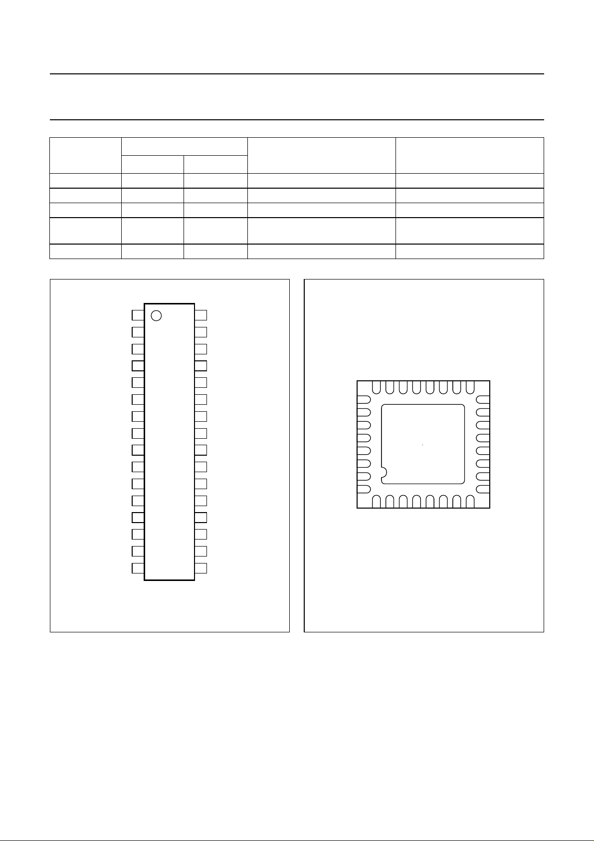
5 ORDERING INFORMATION
TYPE
NUMBER
NAME DESCRIPTION VERSION
PACKAGE
UDA1380TT TSSOP32 plastic thin shrink small outline package; 32 leads;
body width 6.1 mm; lead pitch 0.65 mm
UDA1380HN HVQFN32 plastic, heatsink very thin quad flat package; no leads;
32 terminals; body 5 × 5 × 0.85 mm
SOT487-1
SOT617-1
2002 Sep 16 7
Philips Semiconductors Product specification
Stereo audio coder-decoder
for MD, CD and MP3
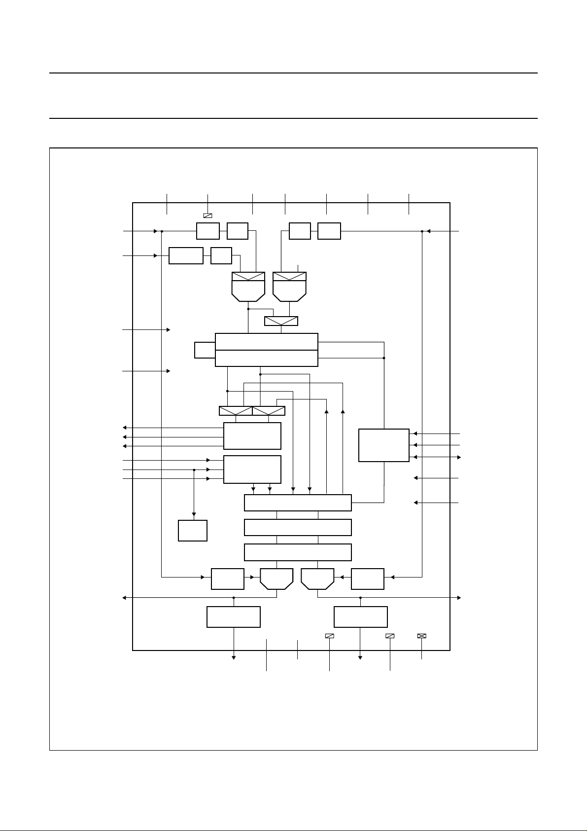
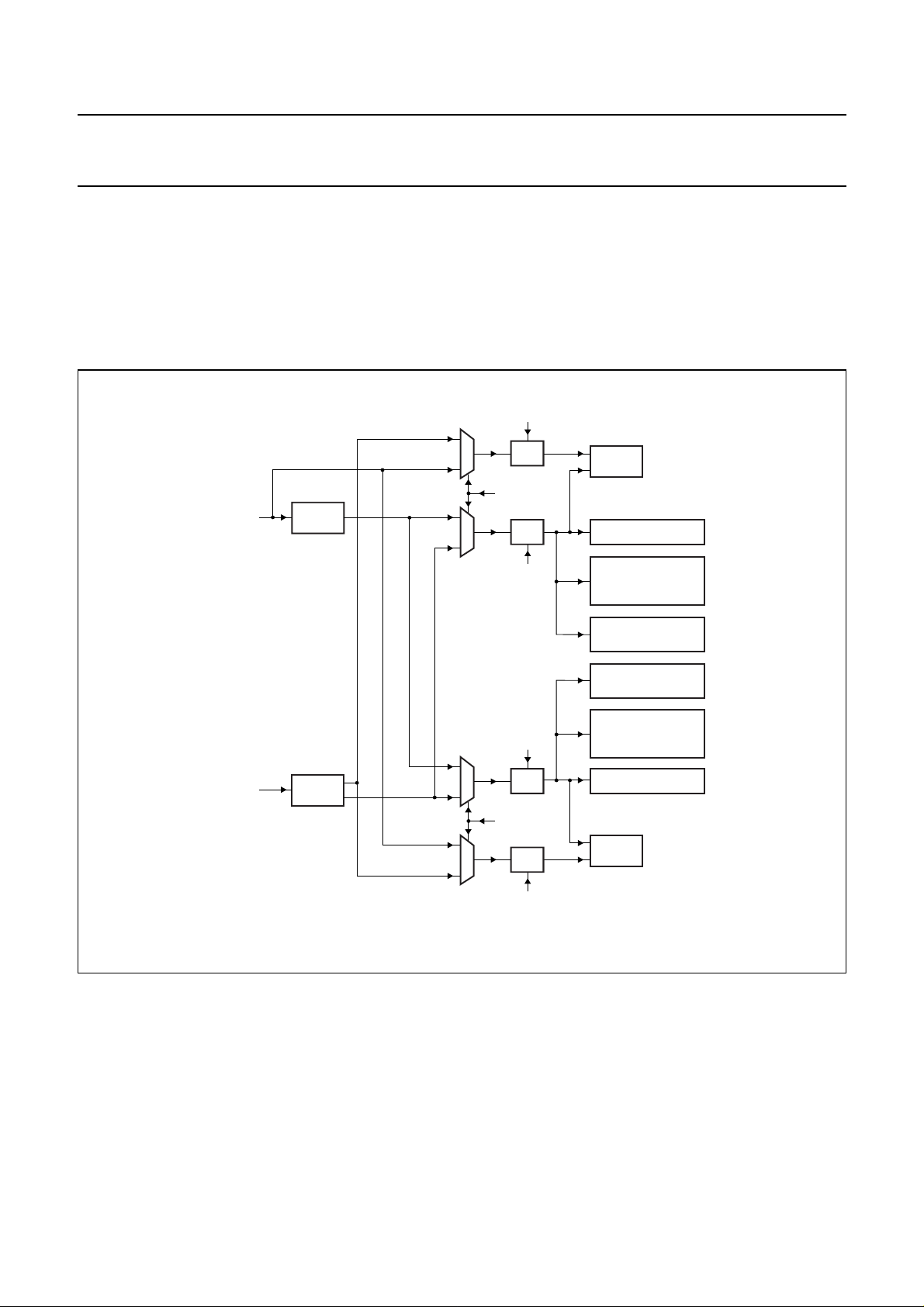
6 BLOCK DIAGRAM
handbook, full pagewidth
VINL
VINM
RESET
SYSCLK
31 (27)
3 (31)
5 (1)
13 (9)
V
DDA(AD)
32 (28)
+29 dB
V
SSA(AD)
AGC
V
30 (26)
SDCPGA PGA
SDCMIC AMP
ADC
DECIMATION FILTER
DC-CANCELLATION FILTER
ADCP
4 (32)
V
ADCN
2 (30)
ADC
SDC
n.c.
V
REF
29 (25)
V
DDD
6 (2)
UDA1380TT
(UDA1380HN)
V
DDA(DA)
26 (22)
1 (29)
UDA1380
VINR
DATAO
BCKO
WSO
BCKI
WSI
DATAI
VOUTL
Pin numbers for UDA1380HN in parentheses.
9 (5)
7 (3)
8 (4)
10 (6)
11 (7)
12 (8)
WSPLL
27 (23)
DATA OUTPUT
INTERFACE
DATA INPUT
INTERFACE
ANA VC
HEADPHONE
DRIVER
DSP FEATURES
INTERPOLATION FILTER
NOISE SHAPER
FSDAC
V
DDA(HP)
FSDAC
22 (18)24 (20)23 (19) 28 (24)
V
REF(HP)
V
HEADPHONE
DRIVER
20 (16) 21 (17)
VOUTRHPVOUTLHP
SSA(HP)
L3 or I2C-BUS
INTERFACE
ANA VC
V
SSA(DA)
V
17 (13)
16 (12)
18 (14)
19 (15)
15 (11)
25 (21)
14 (10)
SSD
L3CLOCK/SCL
L3MODE
L3DATA/SDA
SEL_L3_IIC
RTCB
VOUTR
MGU526
Fig.1 Block diagram.
2002 Sep 16 8
Philips Semiconductors Product specification
Stereo audio coder-decoder
UDA1380
for MD, CD and MP3
7 PINNING
SYMBOL
UDA1380TT UDA1380HN
VINR 1 29 analog pad ADC input right, also connected
V
ADCN
VINM 3 31 analog pad microphone input
V
ADCP
RESET 5 1 5 V tolerant digital input pad;
V
DDD
BCKO 7 3 5 V tolerant digital bidirectional
WSO 8 4 word select output
DATAO 9 5 output pad; push-pull; 5 ns
BCKI 10 6 5 V tolerant digital input pad;
WSI 11 7 word select input
DATAI 12 8 data input
SYSCLK 13 9 system clock 256f
V
SSD
RTCB 15 11 5 V tolerant digital input pad;
L3MODE 16 12 5 V tolerant digital bidirectional
L3CLOCK/SCL 17 13 5 V tolerant digital input pad;
L3DATA/SDA 18 14 I
SEL_L3_IIC 19 15 5 V tolerant digital input pad;
V
SSA(HP)
VOUTRHP 21 17 analog pad headphone output right
V
REF(HP)
VOUTLHP 23 19 analog pad headphone output left
V
DDA(HP)
VOUTR 25 21 analog pad DAC output right
V
DDA(DA)
VOUTL 27 23 analog pad DAC output left
PIN
TYPE DESCRIPTION
to the mixer input of the FSDAC
2 30 analog pad ADC reference voltage
4 32 analog pad ADC reference voltage
pin RESET with pull-down, for
push-pull; TTL with hysteresis;
making Power-On Reset (POR)
pull-down
6 2 digital supply pad digital supply voltage
bit clock output
pad; push-pull input; 3-state
output; 5 ns slew-rate control;
TTL with hysteresis
data output
slew-rate control; CMOS
bit clock input
push-pull; TTL with hysteresis
, 384fs,
s
512fsor 768fs input
14 10 digital ground pad digital ground
test control input, to be connected
push-pull; TTL with hysteresis;
to digital ground in the application
pull-down
L3-bus mode input or pin A1 for
pad; push-pull input; 3-state
I2C-bus slave address setting
output; 5 ns slew-rate control;
TTL with hysteresis
2
L3-bus or I
C-bus clock input
push-pull; TTL with hysteresis
2
C-bus pad; 400 kHz I2C-bus
specification
L3-bus or I2C-bus data input and
output
input channel select
push-pull; TTL with hysteresis
20 16 analog ground pad headphone ground
22 18 analog pad headphone reference voltage
24 20 analog supply pad headphone supply voltage
26 22 analog supply pad DAC analog supply voltage
2002 Sep 16 9
Philips Semiconductors Product specification
Stereo audio coder-decoder
UDA1380
for MD, CD and MP3
SYMBOL
UDA1380TT UDA1380HN
V
SSA(DA)
V
REF
V
SSA(AD)
VINL 31 27 analog pad ADC input left, also connected to
V
DDA(AD)
handbook, halfpage
V
V
RESET
DATAO
SYSCLK
L3MODE
VINR
ADCN
VINM
ADCP
V
DDD
BCKO
WSO
BCKI
WSI
DATAI
V
SSD
RTCB
1
2
3
4
5
6
7
8
UDA1380TT
9
10
11
12
13
14
15
16
PIN
TYPE DESCRIPTION
28 24 analog ground pad DAC analog ground
29 25 analog pad ADC and DAC reference voltage
30 26 analog ground pad ADC analog ground
the mixer input of the FSDAC
32 28 analog supply pad ADC analog supply voltage
V
32
DDA(AD)
31
VINL
handbook, halfpage
DATAI
WSI
BCKI
DATAO
WSO
BCKO
V
DDD
RESET
8
7
6
5
4
3
2
1
SSD
SYSCLK
V
9
10
31
32
VINM
ADCP
V
RTCB
L3MODE
L3CLOCK/SCL
11
13
UDA1380HN
282627
29
30
VINR
ADCN
V
DDA(AD)
V
SSA(HP)
L3DATA/SDA
SEL_L3_IIC
V
16
141215
17
18
19
20
21
22
23
24
25
REF
VINL
V
SSA(AD)
V
VOUTRHP
V
REF(HP)
VOUTLHP
V
DDA(HP)
VOUTR
V
DDA(DA)
VOUTL
V
SSA(DA)
MGW778
MGU525
V
30
SSA(AD)
V
29
REF
V
28
SSA(DA)
27
VOUTL
V
26
DDA(DA)
25
VOUTR
V
24
DDA(HP)
23
VOUTLHP
V
22
REF(HP)
21
VOUTRHP
V
20
SSA(HP)
19
SEL_L3_IIC
18
L3DATA/SDA
17
L3CLOCK/SCL
Fig.2 Pin configuration UDA1380TT.
2002 Sep 16 10
Fig.3 Pin configuration UDA1380HN.
Philips Semiconductors Product specification
Stereo audio coder-decoder
for MD, CD and MP3
8 FUNCTIONAL DESCRIPTION
8.1 Clock modes
There are two clock systems:
• A SYSCLK signal, coming from the system or the SSA1
chip
• A WSPLL which generates the internal clocks from the
incoming WSI signal.
The system frequency applied to pin SYSCLK is
selectable. The options are 256fs, 384fs, 512fsand 768fs.
Thesystemclockmustbelockedinfrequencytothedigital
interface signals.
Remark: Since there is neither a fixed reference clock
available in the IC itself, nor a fixed clock available in the
systemtheICis in, there is no auto sample rate conversion
detection circuitry.
The system can run in several modes, using the two clock
systems:
• Both the DAC and the ADC part can run at the applied
SYSCLK input. In this case the WSPLL is
powered-down
• The ADC can run at the SYSCLK input, and at the same
time the DAC part can run (at a different frequency) at
the clock re-generated from the WSI signal
• The ADC and the DAC can both run at the clock
regenerated from the WSI signal.
UDA1380
8.1.1 WSPLL REQUIREMENTS
TheWSPLLismeant to lock onto the WSI input signal, and
regenerates a 256fsand 128fs signal for the FSDAC and
the interpolator core (and for the decimator if needed).
Since the operating range of the WSPLL is from
75 to 150 MHz, the complete range of 8 to 100 kHz
sampling frequency must be divided into smaller parts, as
given in Table 1, using Fig.4 as a reference. This means
that the user must set the input range of the WSI input
signal.
In case the SYSCLK is used for clocking the complete
system(decimatorincludinginterpolator)theWSPLLmust
be powered-down with bit ADC_CLK via the L3-bus
or I2C-bus.
The SEL_LOOP_DIV[1:0] can be controlled by the PLL1
and PLL0 bits in the L3-bus or I2C-bus register.
handbook, halfpage
DIV1
128f
(digital parts)
256f
(ADC and FSDAC)
s
VCOWSI
PRE1
s
MGU527
Fig.4 WSPLL set-up.
Table 1 WSPLL divider settings
WORD SELECT
FREQUENCY (kHz)
SEL_LOOP_DIV[1:0] PRE1 DIV1
6.25 to 12.5 00 8 1536
12.5 to 25 01 4 1536
25 to 50 10 2 1536
50 to 100 11 2 768
2002 Sep 16 11
VCO FREQUENCY
(MHz)
76 to 153
Philips Semiconductors Product specification
Stereo audio coder-decoder
UDA1380
for MD, CD and MP3
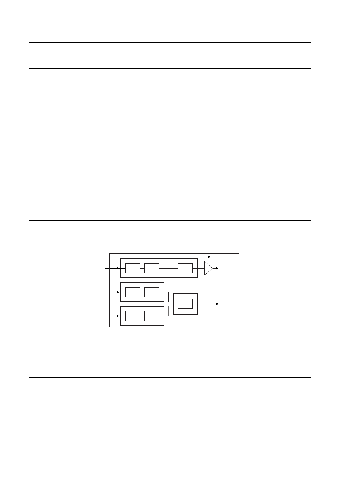
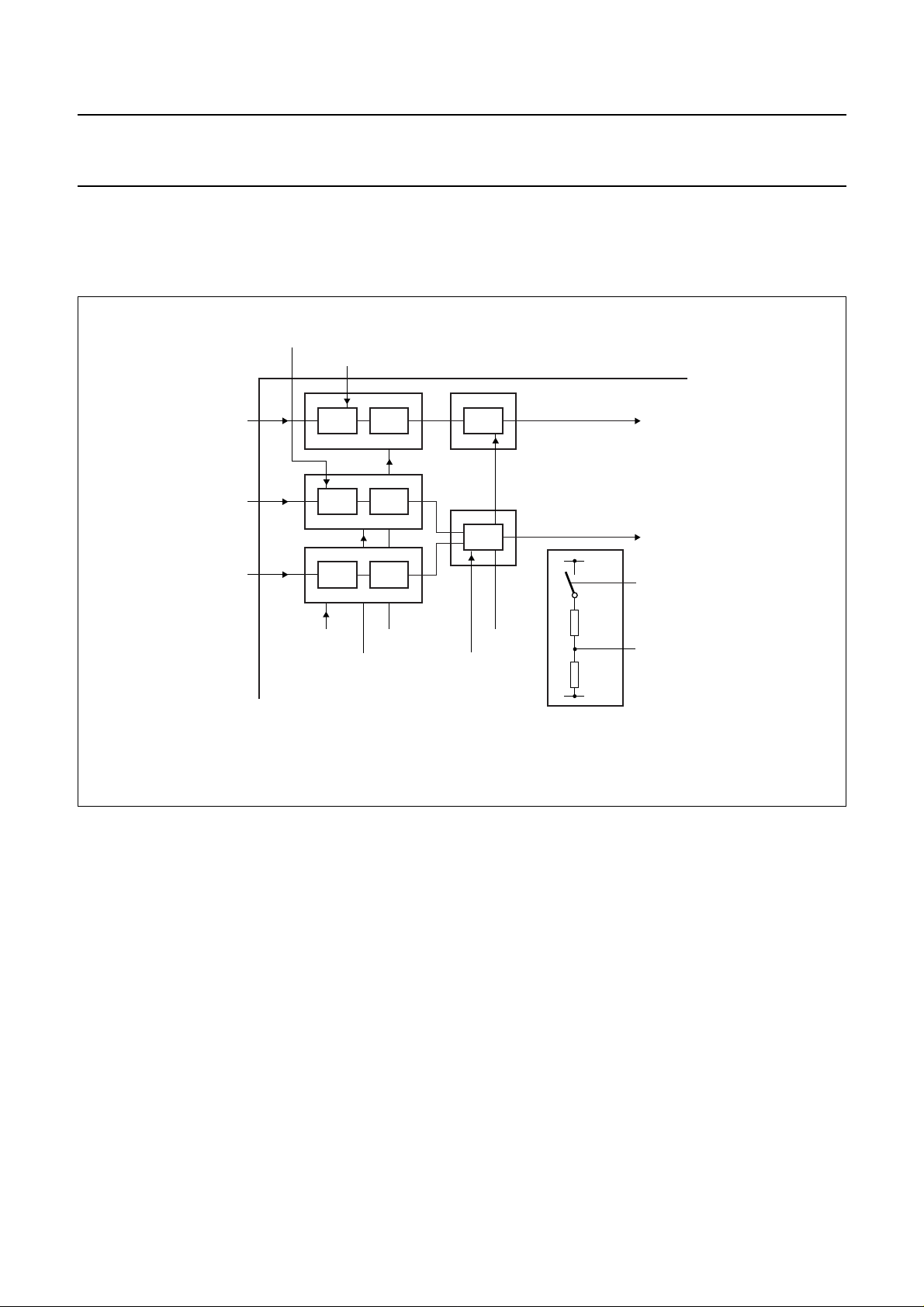
8.1.2 CLOCK DISTRIBUTION
Figure 5 shows the main clock distribution for the SYSCLK domain and the WSPLL clock domain.
For power saving reasons each clock signal inside the system must be controlled and enabled via a separate bit in the
L3-bus and I2C-bus registers (ADC_CLK).
The DAC part of the UDA1380 can operate from 8 to 100 kHz sampling frequency (fs). This applies to the DAC part only;
the ADC part can run from 8 to 55 kHz.
handbook, full pagewidth
SYSCLK
CLK_DIV
256/384/512/768f
128f
s
s
enable clock
ADC_CLK
128f
s
enable
clock
ADC
DECIMATOR
L3 or I2C-BUS
REGISTER
DECIMATOR
I2S-BUS
OUTPUT BLOCK
2
I
INPUT BLOCK
L3 or I2C-BUS
REGISTER
INTERPOLATOR
INTERPOLATOR
FSDAC
MGU528
WSI
WSPLL
256f
enable
clock
s
128f
s
128f
s
DAC_CLK
enable clock
Fig.5 Clock routing for the main blocks inside the coder-decoder.
S-BUS
2002 Sep 16 12
Philips Semiconductors Product specification
Stereo audio coder-decoder
for MD, CD and MP3
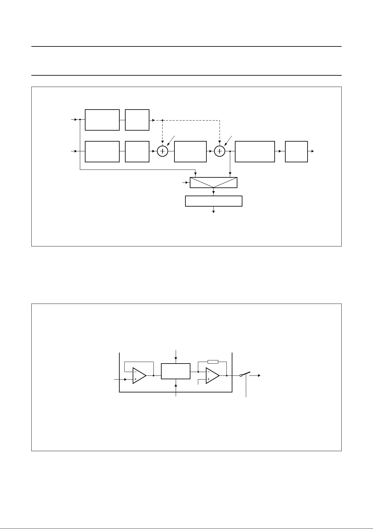
8.2 ADC analog front-end
The analog front-end of the UDA1380 consists of one
stereo ADC with a selector in front of it (see Fig.6). Using
this selector one can either select the microphone input
with the microphone amplifier (LNA) with a fixed 29 dB
gain and VGA (no PGA, since a real microphone amplifier
ismuchbetterwith respect to noise), or the line input which
has a PGA for having 0 or 6 dB gain (for supporting 1 and
2 V (RMS)input).The PGA also provides gain control from
0 to 24 dB in steps of 3 dB.
Remarks:
• TheinputimpedanceofthePGA(lineinput)is12 kΩ,for
the LNA this is 5 kΩ
• TheLNAis standard equipped with a microphone power
supply. Since this normally requires two extra pins, this
feature will not be used inside the UDA1380. Instead,
the microphone supply block is replaced by the VGA
block.
UDA1380
8.2.1 APPLICATIONS AND POWER-DOWN MODES
The following Power-down modes and functional modes
are supported:
• Power-down mode in which the power consumption is
very low (only leakage currents)
In this mode there is no reference voltage at the line
input
• Line input mode, in which the PGA can be used
• Microphone mode, in which the rest of the non-used
PGAs and ADCs are powered-down
• Mixed PGA and LNA mode: one line input and one
microphone input.
More information on the analog frond-end is given in
Section 8.11.1.
handbook, full pagewidth
VINL
1
(29)
31
(27)
3
(31)
PGA ADC
PGA
LNA SDC
SDC
SDC
VINR
VINM
Pin numbers for UDA1380HN in parentheses.
Fig.6 Analog front-end.
8.2.2 LNA WITH VGA
The LNA is equipped with a VGA. The function of the VGA
is to have additional variable analog gain from 0 to 30 dB
in steps of 2 dB. This provides more flexibility in the choice
of the microphone.
SEL_MIC
bitstream
right
ADC
bitstream
left
MGU530
8.2.3 APPLICATIONS WITH 2V(RMS) INPUT
For the line input it is preferable to have 0 dB and 6 dB
gain settings in order to be able to apply both
1 and 2 V (RMS) input signals, using a series resistance.
For this purpose a PGA is used which has0 to 24 dB gain,
in steps of 3 dB.
2002 Sep 16 13
Philips Semiconductors Product specification
Stereo audio coder-decoder
for MD, CD and MP3
In applications in which a 2 V (RMS) input signal is used,
a12kΩresistor must be used in series with the input of the
ADC(see Fig.7). This forms a voltage divider together with
the internal ADC resistor and ensures that the voltage,
applied to the input of the IC, never exceeds 1 V (RMS).
Using this application for a 2 V (RMS) input signal, the
switchmust be set to 0 dB.When a 1 V (RMS) input signal
is applied to the ADC in the same application, the gain
switch must be set to 6 dB.
An overview of the maximum input voltages allowed
againstthepresenceofanexternalresistor and the setting
of the gain switch is given in Table 2; the power supply
voltage is assumed to be 3 V.
handbook, halfpage
input signal
2 V (RMS)
Pin numbers for UDA1380HN in parentheses.
Fig.7 ADC front-end with PGA (line input).
external
resistor
12 kΩ
VINL,
VINR
31,
1
(27,
29)
12 kΩ
V
REF
PGA
V
DDA
= 3 V
MGU529
UDA1380
Table 3 Decimation filter characteristics
ITEM CONDITION VALUE (dB)
Pass-band ripple 0 to 0.45f
Stop band >0.55f
Dynamic range 0 to 0.45f
Digital output
level
8.3.1 O
VERLOAD DETECTION
at 0 dB input
analog
s
s
s
TheUDA1380is equipped with an overload detector which
can be read out from the L3-bus or I2C-bus interface.
In practice the output is used to indicate whenever the
output data, in either the output of the left or right channel,
exceeds −1 dB (the actual figure is −1.16 dB) of the
maximum possible digital swing. When this condition is
detected the output bit OVERFLOW in the L3-bus register
is forced to logic 1 for at least 512fs cycles (11.6 ms at
fs= 44.1 kHz). This time-out is reset for each infringement.
8.3.2 VOLUME CONTROL
The decimator is equipped with a digital volume control.
This volume control is separate for left and right and can
be set with bits ML_DEC [7:0] and bits MR_DEC [7:0] via
the L3-bus or I2C-bus interface. The range is from +24 dB
to −63.5 dB and mutes in steps of 0.5 dB.
0.01
−70
>135
−1.5
Table 2 Application modes using input gain stage
RESISTOR
(12 kΩ)
INPUT GAIN
SWITCH
MAXIMUM
INPUT
VOLTAGE
Present 0 dB 2 V (RMS)
6 dB 1 V (RMS)
Absent 0 dB 1 V (RMS)
6 dB 0.5 V (RMS)
8.3 Decimation filter (ADC)
Thedecimation from 128fsisperformed in two stages. The
first stage realizes a characteristic with a decimation
----------x
xsin
factor of 16. The second stage consists of 3 half-band
filters, each decimating by a factor 2. The filter
characteristics are shown in Table 3.
8.3.3 MUTE
The decimator is equipped with a dB-linear mute which
mutes the signal in 256 steps of 0.5 dB.
8.3.4 AGC FUNCTION
The decimation filter is equipped with an AGC block. This
function is intended, when enabled, to keep the output
signal at a constant level. The AGC can be used for
microphone applications in which the distance to the
microphone is not always the same.
The AGC can be enabled via an L3-bus or I2C-bus bit by
setting the bit to logic 1. In that case it bypasses the digital
volume control.
Via the L3-bus or I2C-bus interface also some other
settings of the AGC, like the attack and decaysettings and
the target level settings, can be made.
Remark: The DC filter before the decimation filter must be
enabled by setting the L3-bus or I2C-bus bit SKIP_DCFIL
to logic 0 when AGC is in operation; otherwise the output
will be disturbed by the DC offset added in the ADC.
2002 Sep 16 14
Philips Semiconductors Product specification
Stereo audio coder-decoder
for MD, CD and MP3
8.4 Interpolation filter (DAC)
The interpolation digital filter interpolates from 1 to 64fsor
to 128fs, by cascading FIR filters, see Table 4. The
interpolator is equipped with several sound features like
volume control, mute, de-emphasis and tone control.
Table 4 Interpolation filter characteristics
ITEM CONDITION VALUE (dB)
Pass-band ripple 0 to 0.45f
Stop band >0.55f
Dynamic range 0 to 0.45f
8.4.1
DIGITAL MUTE
s
s
s
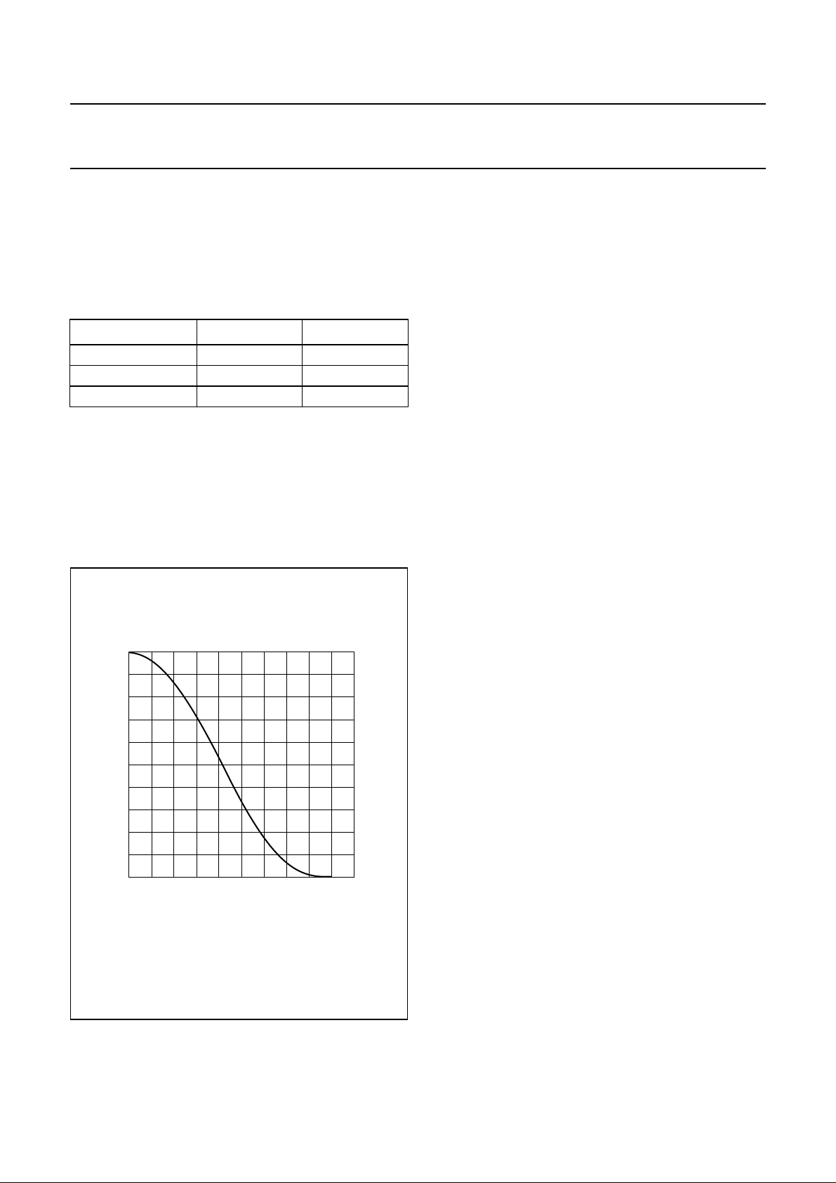
Muting the DAC will result in a cosine roll-off soft mute,
using 4 × 32 = 128 samples in normal mode (or 3 ms at
44.1 kHz sampling frequency). The cosine roll-off curve is
illustrated in Fig.8. These cosine roll-off functions are
implementedfor both the digital mixer and themastermute
inside the DAC data path, see Section 8.8.
handbook, halfpage
1
mute
factor
0.8
0.6
0.4
0.2
0
01051525
±0.025
−60
>135
MGU119
20
t (ms)
UDA1380
8.4.2 S
In addition, there are basic sound features:
• dB-linear volume control using 14-bit coefficients in
steps of 0.25 dB: range 0 to −78 dB maximum
suppression and −∞ dB: applies to both master volume
and mixing volume control
• De-emphasis for 32, 44.1, 48 and 96 kHz for both
channel 1 and 2 (selectable independently)
• Treble, which is selectable gain for high frequencies
(positive gain only), the edge frequency of the treble is
fixed (depends on the sampling frequency). Can be set
for left and right independently:
– Two settings: fc= 1.5 kHz and fc= 3 kHz, assuming
– Both settings have 0 to 6 dB gain range in steps
• Bass boost, which is selectable gain for low frequencies
(positive gain only). The edge frequency of the bass
boost is fixed and depends on the sampling frequency.
Can be set for left and right independently:
– Two settings: fc= 250 Hz and fc= 300 Hz, assuming
– First setting: 0 to 18 dB gain range in steps of 2 dB
– Second setting: 0 to 24 dB gain range in
8.5 Noise shaper
The noise shaper consists of two mono 3rd-order noise
shapers and one time-multiplexed stereo 5th-order noise
shaper.
The order of the noise shaper can be chosen between
3rd-order (which runs at 128fs) and 5th-order (which runs
at 64fs) via bit SEL_NS in the L3-bus or I2C-bus register.
The preferable choice for the noise shaper order is:
• 3rd-order noise shaper is preferred at low sampling
frequencies, for instance between 8 and 32 kHz. This is
for preventing out-of-band noise from the noise shaper
to move into the audio band
• 5th-order noise shaper is normally used at higher
sampling frequencies, normally from 32 to 100 kHz.
OUND FEATURES
sampling frequency is 44.1 kHz
of 2 dB
sampling frequency is 44.1 kHz
steps of 2 dB.
Fig.8 Mute as a function of raised cosine roll-off,
displayed assuming 44.1 kHz.
2002 Sep 16 15
The noise shaper shifts in-band quantization noise to
frequencieswellabovetheaudioband.Thisnoiseshaping
technique enables high signal-to-noise ratios to be
achieved. The noise shaper output is converted into an
analog signal using an FSDAC.

Philips Semiconductors Product specification
Stereo audio coder-decoder
for MD, CD and MP3
8.6 FSDAC
8.6.1 GENERAL INFORMATION
The Filter-Stream Digital-to-Analog Converter (FSDAC) is
a semi-digital reconstruction filter that converts the
1-bit data stream (running at either 64fs for the 5th-order
noiseshaperor128fsforthe3rd-ordernoiseshaper)ofthe
noise shaper into an analog output voltage. The filter
coefficients are implemented as current sources, and are
summed at virtual ground of the output operational
amplifier. In this way very high signal-to-noise
performance and low clock jitter sensitivity are achieved.
A post-filteris not needed due to theinherent filter function
of the DAC. On-board amplifiers convert the FSDAC
output current to an output voltage signal, capable of
driving a line output. The output voltage of the FSDAC
scales proportionally with the power supply voltage.
Remark: When the FSDAC is powered-down, the output
of the FSDAC becomes high impedance.
8.6.2 ANALOG MIXER INPUT
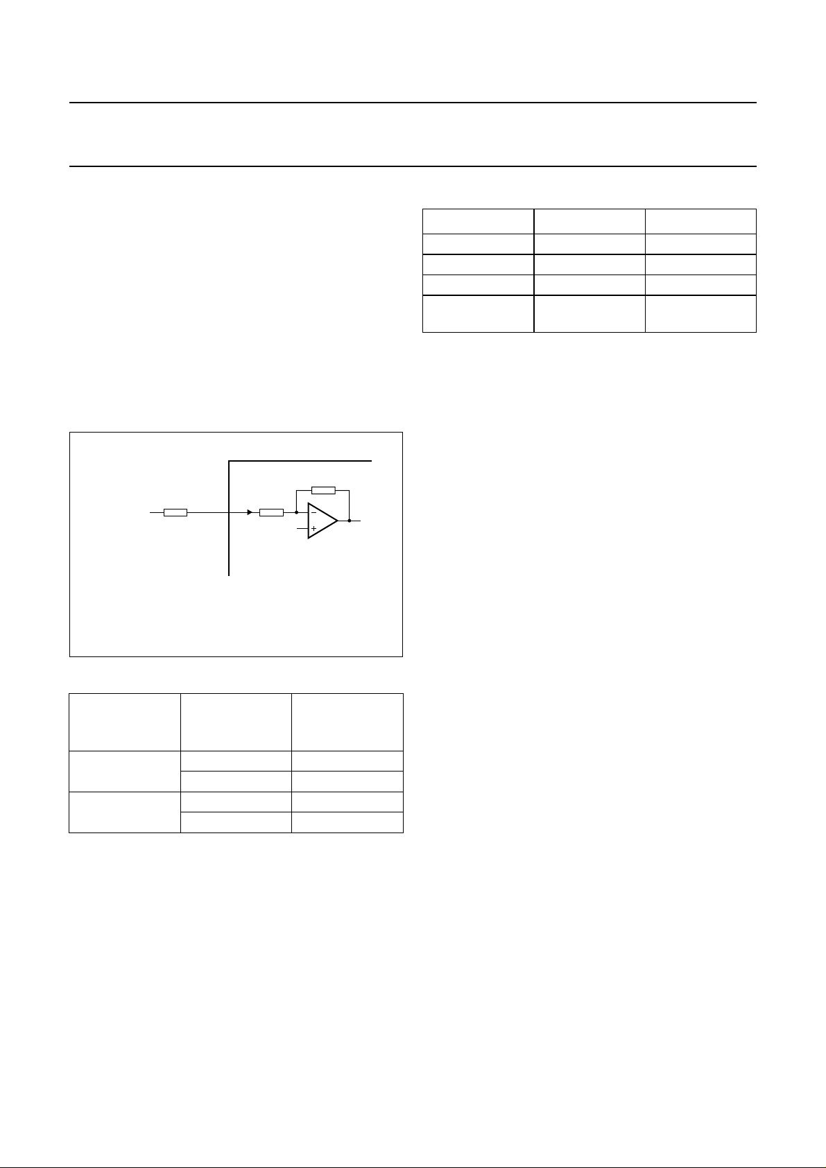
UDA1380
8.7 Headphone driver
The UDA1380 is equipped with a headphone driver which
can deliver 36 mW (at 3.0 V power supply) into a 16 Ω
load.
The headphone driver does not need external
DC decoupling capacitors because it can be DC coupled
with respect to a special headphone output reference
voltage. This saves two external capacitors (which is quite
useful in a portable device).
The headphone driver is equipped with short-circuit
protection on all three operationalamplifiers (left, right and
the virtual ground). Each of the operational amplifiers has
a signalling bit which becomes logic 1 in case the limiter is
activated, for instance in case of a short-circuit. This
means the microcontroller in the system can poll the
L3-bus or I2C-bus register of the headphone driver and as
soon as, and for as long as, the short-circuit detection bits
are activated, the microcontroller can signal the user that
something is wrong or power-down the headphone driver
(for instance, for energy-saving purposes).
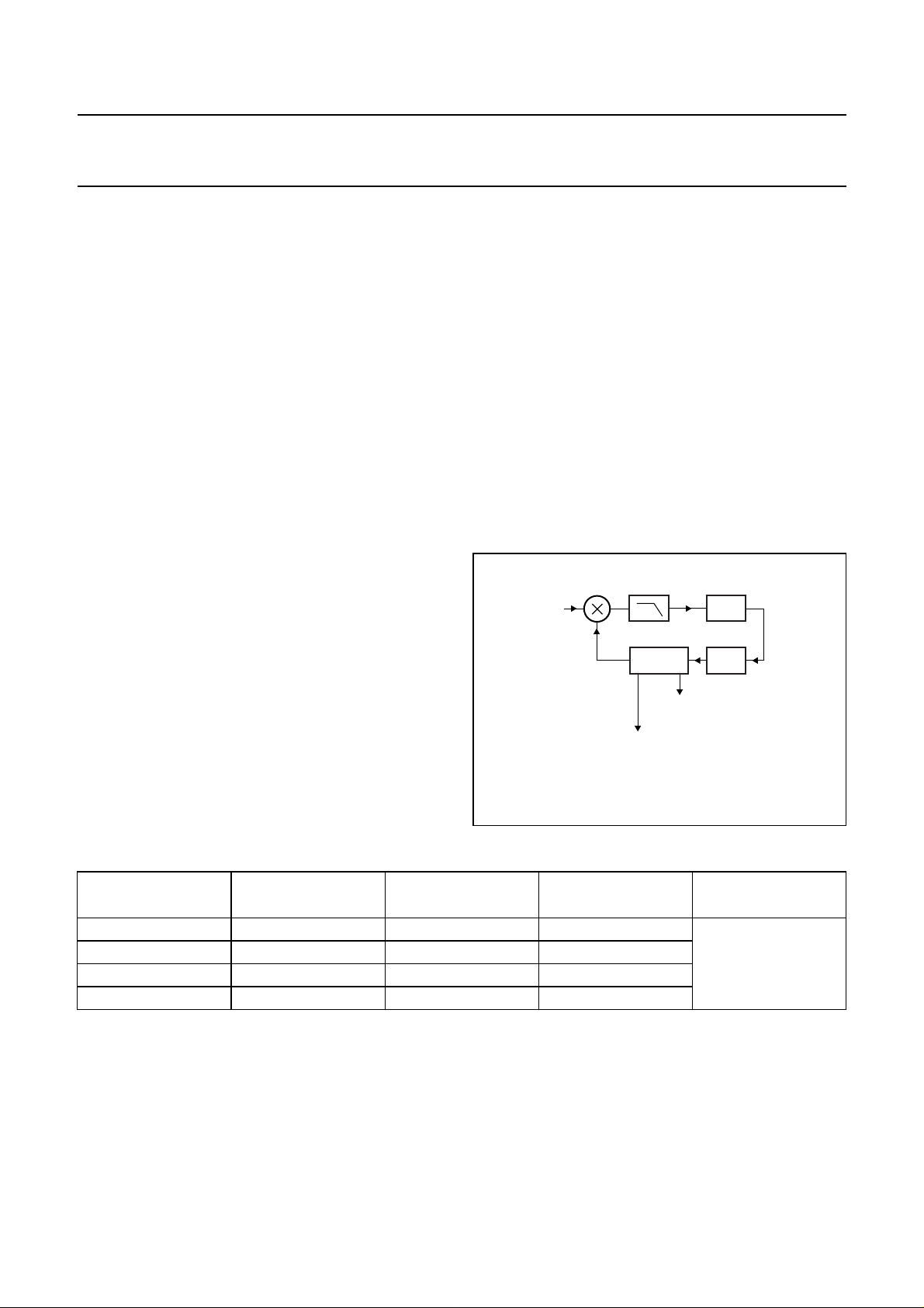
The FSDAC has a mixer input, which makes it possible to
mix an analog signal to the output signal of the FSDAC
itself. In schematic form this is given in Fig.9.
This mixer input can be used for instance for mixing-in a
GSM signal or an FM signal directly to the line output.
In the UDA1380, the mixer input is connected from the
ADC line input via an AVC unit.
Remark: Before the AVC unit can be used stand-alone,
meaning without the digital part running, first the DAC part
must be initialised in order to have the DAC output
generating zero current. Otherwise the signal will be
clipped.
handbook, halfpage
bitstream
to analog mixer input
FSDAC
MGU531
Fig.9 Mixing signals to the FSDAC output
(analog domain).
Remark: To improve headphone channel separation
performance,thedistancebetweenV
REF(HP)
andthemicro
speaker port must be minimized.
8.8 Digital and analog mixers (DAC)
8.8.1 DIGITAL MIXER
The ADC output signal and digital input signal can be
mixedwithoutexternalDSP as shown in Fig.10. This mixer
can be controlled via the microcontroller interface, and
must only be enabled when the ADC and the DAC are
running at the same frequency. In addition, the mixer
output signal can also be applied to the I2S-bus output
interface.
2002 Sep 16 16
Philips Semiconductors Product specification
Stereo audio coder-decoder
for MD, CD and MP3
data from
handbook, full pagewidth
decimation
filter
(channel 2)
from
digital
data input
(channel 1)
DE-EMPHASIS
DE-EMPHASIS
VOLUME
AND
MUTE
VOLUME
AND
MUTE
1f
s
mixing before
sound features
BASS-BOOST
AND
TREBLE
SEL_SOURCE
I2S-BUS OUTPUT BLOCK
Fig.10 Digital mixer (DAC).
mixing after
sound features
INTERPOLATION
FILTER
2f
s
UDA1380
master
VOLUME
AND
MUTE
to
interpolation
filter
MGU532
8.8.2 ANALOG MIXER
The analog mixer, which uses the mixer input of the FSDAC, can mix a signal into the FSDAC output signal via an AVC
unit (see Fig.11). The mixer can be used to mix a signal into the FSDAC output signal and play it via the headphone
driver without the complete coder-decoder running. The analog control range is 0 to −64.5 dB and mutes in steps
of 1.5 dB, with a gain of 16.5 dB (so actually the range is from +16.5 dB to −48 dB plus mute).
handbook, full pagewidth
from analog
front-end
AVC[5:0] L3 or I
PON_AVC
RESISTOR
NETWORK
2
C-bus control bits
enable mixer
(EN_AVC)
to FSDAC
mixer input
MGU533
Fig.11 Analog mixer configuration.
2002 Sep 16 17
Philips Semiconductors Product specification
Stereo audio coder-decoder
for MD, CD and MP3
8.9 Application modes
The operation mode can be set with pin SEL_L3_IIC,
either to L3-bus mode (LOW) or to the I2C-bus mode
(HIGH) as given in Table 5.
For all features in microcontroller mode see Chapter 9.
Table 5 Pin function in the selected mode
PIN
L3CLOCK/SCL L3CLOCK SCL
L3MODE L3MODE A1
L3DATA/SDA L3DATA SDA
Remark: In the I
the LSB bit of the address of the UDA1380. In
L3-bus mode this bit is not available, meaning the device
has only one L3-bus device address.
L3-BUS MODE
SEL_L3_IIC = L
2
C-bus mode there is a bit A1 which sets
I2C-BUS MODE
SEL_L3_IIC = H
UDA1380
8.11 Power-down requirements
The following blocks have power-down control via the
L3-bus or I
• Microphone amplifier (LNA) including its Single-Ended
to Differential Converter (SDC) and VGA
• ADC plus SDC and the PGA, for left and right separate
• Bias generation circuit for the front-end and the FSDAC
• Headphone driver
• WSPLL
• FSDAC.
Clocksofthe decimator, interpolator and the analog blocks
have separate enable and disable controls.
2
C-bus interface:
8.10 Power-on reset
The UDA1380 has a dedicated pin RESET, which has a
pull-down resistor. This way a Power-on reset circuit can
be made with a capacitor and a resistor at the pin. The
internal pull-down resistor cannot be used because of the
5 V tolerant nature of the pad. The pull-down resistor is
shielded from the outside world by a transmission gate in
order to support 5 V tolerance.
The reset timing is determined by the external capacitor
and resistor which are connected to the pin RESET, and
the internal pull-down resistor. By the Power-on reset, all
the digital sound processing features and the system
controlling features are set to the default setting of the
L3-bus and I2C-bus control modes.
Remark: The reset time should be at least 1 µs, and
during the reset time the system clock should be running.
Incase the WSPLL is selected as theclock source, a clock
must be connected to the SYSCLK input in order to have
proper reset of the L3-bus or I2C-bus registers. This is
because by default the clock source is set to SYSCLK.
2002 Sep 16 18
Philips Semiconductors Product specification
Stereo audio coder-decoder
UDA1380
for MD, CD and MP3
8.11.1 ANALOG FRONT-END
Figure 12 shows the power control inside the analog front-end. The control of all power-on pins of the ADC front-end is
done via separate L3-bus or I2C-bus bits.
handbook, full pagewidth
PGA_GAINCTRLL
VINL
1
(29)
31
(27)
3
(31)
VINR
VINM
PGA_GAINCTRLR
PGA
PGA
LNA SDC
SDC
SDC
ADC
ADC
bitstream
right
bitstream
left
PON_BIAS
PON_PGAR PON_ADCRPON_LNA
PON_PGAL PON_ADCL
Pin numbers for UDA1380HN in parentheses.
Fig.12 Analog front-end power-down.
8.11.2 FSDAC POWER CONTROL
The FSDAC block has power-on pins: one of which shuts
down the DAC itself, but leaves the output still at V
REF
voltage (which is half the power supply). This function is
set by the bit PON_DAC in the L3-bus or I2C-bus register.
A second L3-bus or I2C-bus bit shuts down the complete
bias circuit of the FSDAC, via bit PON_BIAS in the
L3-bus or I2C-bus register. This bit PON_BIAS acts the
same as given in Fig.12 for the analog front-end.
8.12 Plop prevention
Plops are ticks and other strange sounds, that can occur
when a part of a device is powered-up or powered-down,
or when switching between modes is done.
Some ways to prevent plops from occurring are:
• When the FSDAC or headphone driver must be
powered-down, first a digital mute is applied. After that
V
REF
FE
BIAS
MGU534
the FSDAC or headphone driver can be powered-down.
In case the FSDAC or headphone driver must be
powered-up,first the analog part is switched on,thenthe
digital part is demuted
• When the ADC must be powered-down, a digital mute
sequence must be applied. When the digital output
signal is completely muted, the ADC can be
powered-down. In case the ADC must be powered-up,
firsttheanalogpartmustbepowered-up,then the digital
part must be demuted
• When there is a change of for example clock divider
settings or clock source (selecting between SYSCLK
and WSPLL clock), then also digital mute for that block
(either decimator or interpolator) should be used.
Remark: All items mentioned in Section 8.12 are not
‘hard-wired’ implemented, but to be followed by the users
as a guideline for plop prevention.
2002 Sep 16 19

Philips Semiconductors Product specification
Stereo audio coder-decoder
for MD, CD and MP3
8.13 Digital audio data input and output
The supported audio formats for the control modes are:
• I2S-bus
• MSB-justified
• LSB-justified, 16 bits
• LSB-justified, 18 bits
• LSB-justified, 20 bits
• LSB-justified, 24 bits (only for the output interface).
The bit clock BCK can be up to 128fs, or in other words the
BCK frequency is 128 times the WS frequency or less:
f
≤ 128f
BCK
Remark: The WS edge must coincide with the negative
edge of the BCK at all times, for proper operation of the
digital I/O data interface. Figure 13 shows the interface
signals.
8.13.1 DIGITAL AUDIO INPUT INTERFACE
The digital audio input interface is slave only, meaning the
system must provide the WSI and BCKI signals (next to
the DATAI signal).
Either the WSPLL locks onto the WSI signal and provides
the internal clocks for the interpolator and the FSDAC, or
a system clock must be applied which must be in
frequency lock to the digital data input interface signals.
8.13.2 DIGITAL AUDIO OUTPUT INTERFACE
The digital audio output interface can be either master or
slave. The data source for the data output can be selected
from either the decimator (ADC front-end) or the digital
mixer output.
Remark: The digital mixer output is only valid if both the
decimator and the interpolator run at the same clock:
• In slave mode the signals on pins BCKO, WSO and
SYSCLK must be applied from the application (signals
mustbein frequency lock) and the UDA1380 returns the
DATAO signal from the decimator. The applied signal
from pin BCKO can be for instance: 32fs, 48fs, 64fs,
96fsor 128f
• In master mode the SYSCLK signal must be applied
from the system, but the UDA1380 returns with the
BCKO, WSO and the DATAO signals. For the BCKO
clock, there are 2 general rules:
– Whenthe SYSCLK is either 256fsor512fs,the BCKO
– Whenthe SYSCLK is either 384fsor 768fs,the BCKO
WS
s
frequency is supposed to be 64f
signal should be 48fs.
s
UDA1380
The slave and master modes can be selected by the
bit Serial Interface Mode (SIM) in the L3-bus or I2C-bus
interface.
9 L3-BUS INTERFACE DESCRIPTION
The UDA1380 has an L3-bus microcontroller
interface mode. Controllable system and digital sound
processing features are:
• Software reset
• System clock frequency (selection between 256fs,
384fs, 512fsand 768fs clock divider settings)
• Clock mode setting, for instance, which block runs at
which clock, and clock enabling
• Power control for the WSPLL
• Data input and data output format control, for input and
output independently including data source selection for
the digital output interface
• ADC features:
– Digital mute
– AGC enable and settings
– Polarity control
– Input line amplifier control (0 to 24 dB in steps of
3 dB)
– DC filtering control
– Digital gain control (+24 to −63 dB gain in steps of
0.5 dB) for left and right
– Power control
– VGA of the microphone input
– Selection of line or microphone input
• DAC and headphone driver features:
– Power control FSDAC and headphone driver
– Polarity control
– Mixing control (only available when both decimator
and interpolator run at the same speed). This
includes the mixer volumes, mute and mixer position
switch
– De-emphasis control
– Master volume and balance control
– Flat/minimum/maximum settings for the bass boost
and treble
– Tone control: bass boost and treble
– Master mute control
– Headphone driver short-circuit protection status bits.
2002 Sep 16 20
Philips Semiconductors Product specification
Stereo audio coder-decoder
for MD, CD and MP3
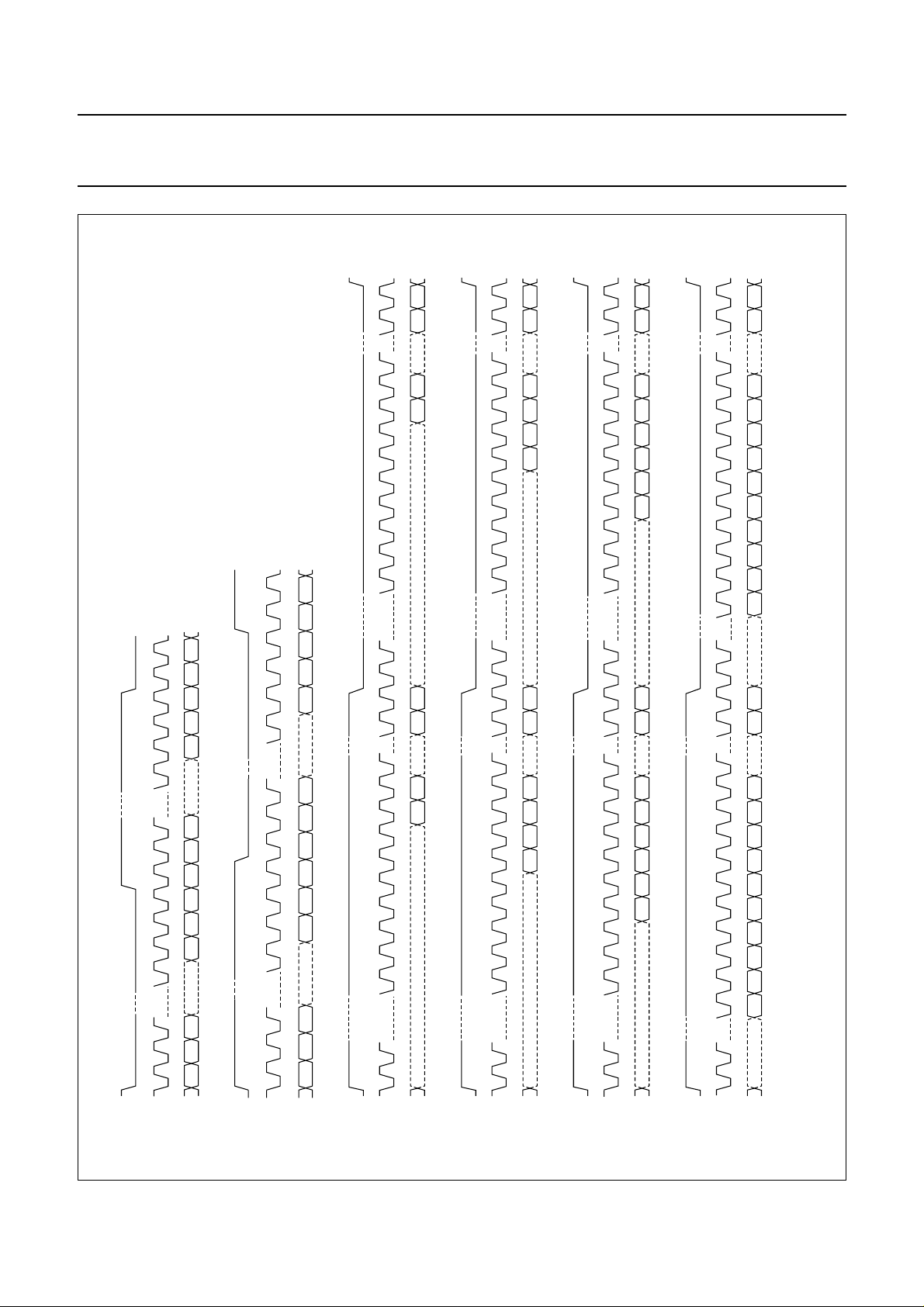
RIGHT
UDA1380
MBL121
B15 LSB
15 2 1
16
MSB B2
RIGHT
B17 LSB
16 1518 17 2 1
MSB B2 B3 B4
RIGHT
B19 LSB
1518 1720 19 2 1
16
MSB B2 B3 B4 B5 B6
RIGHT
B23 LSB
1518 1720 1922 212324 21
16
B5 B6 B7 B8 B9 B10
B3 B4
B2
> = 8
dbook, full pagewidth
RIGHT
3
21> = 812 3
LEFT
MSB MSBB2
S-BUS FORMAT
2
I
MSB B2
RIGHT
LEFT
MSB
LSB
B15
LSB-JUSTIFIED FORMAT 16 BITS
321321
15 2 1
B2
16
MSB
LSB
B17
LSB-JUSTIFIED FORMAT 18 BITS
1518 17 2 1
16
LSB
B19
LSB-JUSTIFIED FORMAT 20 BITS
1518 1720 19 2 1
16
LSB
B23
LSB-JUSTIFIED FORMAT 24 BITS
1518 1720 1922 212324 2 1
16
Fig.13 Serial interface input and output formats.
> = 8 > = 8
MSB-JUSTIFIED FORMAT
LEFT
MSB B2 MSBLSB LSB MSB B2B2
LEFT
MSB B2 B3 B4
LEFT
MSB B2 B3 B4 B5 B6
LEFT
B5 B6 B7 B8 B9 B10
B3 B4
B2
MSB
This text is here in white to force landscape pages to be rotated correctly when browsing through the pdf in the Acrobat reader.This text is here in
_white to force landscape pages to be rotated correctly when browsing through the pdf in the Acrobat reader.This text is here inThis text is here in
white to force landscape pages to be rotated correctly when browsing through the pdf in the Acrobat reader. white to force landscape pages to be ...
2002 Sep 16 21
WS
BCK
DATA
WS
BCK
DATA
WS
BCK
DATA
WS
BCK
DATA
WS
BCK
DATA
WS
BCK
DATA

Philips Semiconductors Product specification
Stereo audio coder-decoder
for MD, CD and MP3
9.1 Introduction
Theexchange of data and control information betweenthe
microcontroller and the UDA1380, is accomplished
through a serial hardware interface comprising the
following pins:
L3DATA/SDA: microcontroller interface data line
L3MODE: microcontroller interface mode line
L3CLOCK/SCL: microcontroller interface clock line.
Information transfer via the microcontroller bus is
organized LSB first, and in accordance with the so called
‘L3’ format, in which two different modes of operation can
be distinguished: address mode and data transfer mode.
Inside the microcontroller there is a hand-shake
mechanism which takes care of proper data transfer from
themicrocontrollerclock,tothe destination clock domains.
This means that when data is sent to the microcontroller
interface, the system clock must be running.
9.2 Device addressing
The device addressing mode is used to select a device for
subsequent data transfer. The address mode is
characterized by the signal on pin L3MODE being LOW
and a burst of 8 pulses on pin L3CLOCK/SCL,
accompanied by 8 bits. The fundamental timing is shown
in Figs 14 and 15.
Basically, two types of transfer can be defined:
data transfer to the device, and data transfer from the
device, as given in Table 6.
Table 6 Selection of data transfer
DOM
BIT 1
Table 6 shows that there are two types of data transfers:
DATA and STATUS which can be read and written.
Table 6 also shows that the DATA and STATUS read and
write actions are combined.
DOM
BIT 0
0 0 not used
0 1 not used
1 0 DATA and STATUS write or pre-read
1 1 DATA and STATUS read
TRANSFER
UDA1380
The device address consists of one byte, which is split-up
in two parts:
• Bits 7 to 2 represent a 6-bit device address. In the
UDA1380 this is 000001
• Bits 1 to 0 called Data Operation Mode, or DOM bits,
represent the type of data transfer according to Table 6.
9.3 Slave address
The UDA1380 acts as a slave receiver or a slave
transmitter.Therefore the signals L3CLOCK and L3MODE
are only input signals. The data signal L3DATA is a
bidirectional line. The UDA1380 slave address is shown in
Table 7.
Table 7 L3 slave address
(MSB) BIT (LSB)
000001
9.4 Register addressing
After sending the device address, including the flags (the
DOM bits) whether information is read or written, one byte
is sent with the destination register address using 7 bits,
and one bit which signals whether information will be read
or written. The fundamental timing for L3 is given in Fig.19.
Basically there are three forms for register addressing:
• Register addressing for L3 write: the first bit is a logic 0
indicating a write action to the destination register,
followed by seven register address bits
• Prepare read addressing: the first bit of the byte is
logic 1; signalling data will be read from the register
indicated
• The read action itself: in this case the device returns a
register address prior to sending data from that register.
When the first bit of the byte is logic 0, the register
address was valid, in case the first bit is a logic 1 the
register address was invalid.
Remarks:
• Each time a new destination address needs to be
written, the device address must be sent again
• When addressing the device for the first time after
power-upof the device, at least oneL3 clock-cycle must
be given to enable the L3 interface.
2002 Sep 16 22

Philips Semiconductors Product specification
Stereo audio coder-decoder
UDA1380
for MD, CD and MP3
9.5 Data write mode
For writing data to a device, four bytes must be sent. Figure 14 explains the data write mode in a signal diagram:
• One byte with the device address, being ‘00000110’, which is including the LSB code 01 for signalling write to the
device
• One byte starting with a logic 0 for signalling write, followed by 7 bits indicating the destination address
• Two data bytes.
The SYSCLK signal must be applied in data write mode.
Table 8 L3 write data
L3 MODE DATA TYPE
Addressing mode device address 0 1 1 0 0 0 0 0
Data transfer 1 register address 0 A6 A5 A4 A3 A2 A1 A0
Data transfer 2 MS data byte D15 D14 D13 D12 D11 D10 D9 D8
Data transfer 3 LS data byte D7 D6 D5 D4 D3 D2 D1 D0
Notes
1. First bit in time.
2. Last bit in time.
(1)
0
1234567
BIT
(2)
9.6 Data read mode
For reading from the device, first a prepare-read must be
done. After this, the device address is sent again. The
device then returns with the register address, indicating
whether the address was valid or not, and the data of the
register. The following five steps explain this procedure,
and an example of transmission is given in Fig.15.
• One byte with the device address, being ‘00000110’,
whichis including the LSB code 01 for signallingwrite to
the address
• One byte is sent with the register address from which it
needs to be read. This byte starts with a logic 1, which
indicates that there will be a read action fromthe register
• One byte with the device address including ‘11’ is sent
to the device, being 00000111. The ‘11’ indicates that
the device must write data to the microcontroller, then
the microcontroller frees the L3DATA-bus so the
UDA1380 can send the register address byte and its
two-byte contents
• The device now writes the requested register address
on the bus, indicating whether the requested register
was valid or not (logic 0 means valid, logic 1 means
invalid)
• The device writes the data from the requested register
on the bus, being two bytes.
The SYSCLK signal must be applied in data read mode.
2002 Sep 16 23

Philips Semiconductors Product specification
Stereo audio coder-decoder
UDA1380
for MD, CD and MP3
Table 9 L3 prepare read data
L3 MODE DATA TYPE
Addressing mode device address 01100000
Data transfer 1 register address 1 A6 A5 A4 A3 A2 A1 A0
Notes
1. First bit in time.
2. Last bit in time.
Table 10 L3 read data
L3 MODE DATA TYPE
Addressing mode device address 1 1 1 0 0 0 0 0
Data transfer 1;
note 3
Data transfer 2;
note 3
Data transfer 3;
note 3
register address 0: valid
MS data byte D15 D14 D13 D12 D11 D10 D9 D8
LS data byte D7 D6 D5 D4 D3 D2 D1 D0
(1)
0
(1)
0
1: invalid
1234567
1234567
A6 A5 A4 A3 A2 A1 A0
BIT
(2)
BIT
(2)
Notes
1. First bit in time.
2. Last bit in time.
3. Data transfer from the UDA1380 to the microcontroller.
2002 Sep 16 24

Philips Semiconductors Product specification
Stereo audio coder-decoder
for MD, CD and MP3
MGU535
data byte 1 data byte 2
UDA1380
MGU536
data byte 1 data byte 2
L3CLOCK
register address
device address
L3MODE
write
Fig.14 Data write mode for L3 version 2.
10
0
DOM bits
L3DATA
0/1
valid/non-valid
Fig.15 Data read mode for L3 version 2.
register address device address register address
1
read
prepare read send by the device
device address
111
0
DOM bits
This text is here in white to force landscape pages to be rotated correctly when browsing through the pdf in the Acrobat reader.This text is here in
_white to force landscape pages to be rotated correctly when browsing through the pdf in the Acrobat reader.This text is here inThis text is here in
white to force landscape pages to be rotated correctly when browsing through the pdf in the Acrobat reader. white to force landscape pages to be ...
2002 Sep 16 25
L3CLOCK
L3MODE
L3DATA

Philips Semiconductors Product specification
Stereo audio coder-decoder
for MD, CD and MP3
10 I2C-BUS INTERFACE DESCRIPTION
The UDA1380 supports I2C-bus microcontroller interface
mode as well as the L3-bus mode; all features can be
controlled by the microcontroller with the same register
addresses as in the L3-bus mode.
Theexchange of data and control information betweenthe
microcontroller and the UDA1380 in I2C-bus mode is
accomplished through a serial hardware interface
comprising the following pins:
L3CLOCK/SCL: microcontroller interface clock line,
SCL
L3MODE: sets the bit A1of the I2C-bus device address
L3DATA/SDA: microcontroller interface data line, SDA.
Figure 20 shows the clock and data timing of the I2C-bus
transfer.
10.1 Addressing
Before any data is transmitted on the I2C-bus, the device
whichshouldrespondisaddressedfirst.Theaddressingis
always done with the first byte transmitted after the start
procedure. The UDA1380 device address is
[A6 to A0] 00110(A1)0, with bit A1 as the address
selection bit (two addresses possible).
UDA1380
10.1.1 D
The UDA1380 acts as either a slave receiver or a slave
transmitter.Therefore the clock signal SCL is only an input
signal.Thedatasignal SDA is a bidirectional line. Table 11
shows the device address of the UDA1380.
The device can be set to one of the two addresses by
using bit A1 (which is pin L3MODE) to select.
Table 11 I
(MSB) BIT (LSB)
10.1.2 R
Table 12 shows the register address format of the
UDA1380. The register mapping in I2C-bus mode is the
same as for the L3-bus interface.
Table 12 I
(MSB) BIT (LSB)
EVICE ADDRESS (PIN A1)
2
C-bus device address
00110A10R/
EGISTER ADDRESS
2
C-bus register address
0 A6A5A4A3A2A1 A0
W
2002 Sep 16 26

Philips Semiconductors Product specification
Stereo audio coder-decoder
for MD, CD and MP3
UDA1380
STOP
C-bus configuration for a WRITE cycle. The WRITE cycle is used to write the data to the internal registers. The device and register
2
LS data
byte
auto increment if repeated n groups of 2 bytes are transmitted
C-bus mode
2
MS data
byte
ADDRESS
REGISTER
C-bus and the microcontroller can generate a stop condition (P).
2
R/W
DEVICE
INITIAL BYTE ACKNOWLEDGE FROM UDA1380
ADDRESS
This text is here in white to force landscape pages to be rotated correctly when browsing through the pdf in the Acrobat reader.This text is here in
_white to force landscape pages to be rotated correctly when browsing through the pdf in the Acrobat reader.This text is here inThis text is here in
white to force landscape pages to be rotated correctly when browsing through the pdf in the Acrobat reader. white to force landscape pages to be ...
10.2 WRITE cycle
Table 13 shows the I
2002 Sep 16 27
by the microcontroller.
addresses are one byte each, the setting data is always a pair of two bytes.
The format of the WRITE cycle is as follows:
1. The microcontroller starts with a start condition (S).
2. The first byte (8 bits) contains the device address ‘00110A10’ and a logic 0 (WRITE) for the bit R/W.
3. This is followed by an acknowledge (A) by the UDA1380.
4. After this the microcontroller writes the register address (ADDR) (8 bits) where the writing of the register content of the UDA1380 must start.
5. The UDA1380 acknowledges this register address (A).
6. The UDA1380 sends the two-bytes data with the Most Significant (MS) byte first, and then the Least Significant (LS) byte, each time acknowledged
7. The UDA1380 stops this cycle by generating an acknowledge (A).
8. Finally, the UDA1380 frees the I
Table 13 Master transmitter writes to UDA1380 registers in the I
S 00110A10 0 A ADDR A MS1 A LS1 A ... A ... A MSn A LSn A P
START

Philips Semiconductors Product specification
Stereo audio coder-decoder
for MD, CD and MP3
UDA1380
LS data
byte
auto increment if repeated n groups of 2 bytes are transmitted
MSdata
byte
C-bus mode
2
R/W
ADDRESS
REGISTER
C-bus and the microcontroller can generate a stop condition (P).
2
C-bus configuration for a READ cycle. The READ cycle is used to read the data values from the internal registers.
2
R/W
This text is here in white to force landscape pages to be rotated correctly when browsing through the pdf in the Acrobat reader.This text is here in
_white to force landscape pages to be rotated correctly when browsing through the pdf in the Acrobat reader.This text is here inThis text is here in
white to force landscape pages to be rotated correctly when browsing through the pdf in the Acrobat reader. white to force landscape pages to be ...
10.3 READ cycle
Table 14 shows the I
2002 Sep 16 28
acknowledged by the microcontroller.
3. This is followed by an acknowledge (A) by the UDA1380.
4. After this the microcontroller writes the register address (ADDR) where the reading of the register content of the UDA1380 must start.
5. The UDA1380 acknowledges this register address.
6. Then the microcontroller generates a repeated start (Sr).
The format of the READ cycle is as follows:
1. The microcontroller starts with a start condition (S).
2. The first byte (8 bits) contains the device address ‘00110A10’ and a logic 0 (WRITE) for the bit R/W.
7. Then the microcontroller generates the device address ‘00110A10’ again, but this time followed by a logic 1 (READ) of the bit R/W.
8. The UDA1380 sends the two-bytes register contents with the Most Significant (MS) byte first, and then the Least Significant (LS) byte, each time
9. The microcontroller stops this cycle by generating a negative acknowledge (NA).
Table 14 Master transmitter reads from the UDA1380 registers in the I
10. Finally, the UDA1380 frees the I
DEVICE
INITIAL BYTE ACKNOWLEDGE FROM UDA1380 ACKNOWLEDGE FROM MICROCONTROLLER
ADDRESS
S 00110A10 0 A ADDR A Sr 00110A10 1 A MS1 A LS1 A ... A ... A MSn A LSn NA P

Philips Semiconductors Product specification
Stereo audio coder-decoder
for MD, CD and MP3
11 REGISTER MAPPING
Table 15 Register map of control settings (write)
REGISTER
ADDRESS
2
System settings (running at the L3-bus or I
00H evaluation modes, WSPLL settings, clock divider and clock selectors
2
01H I
02H power control settings
03H analog mixer settings
04H reserved
Interpolation filter (running at 128f
10H master volume control
11H mixer volume control
12H mode selection, left and right bass boost, and treble settings
13H master mute, channel 1 and channel 2 de-emphasis and channel mute
14H mixer, silence detector and interpolation filter oversampling settings
Decimator (running at 128f
20H decimator volume control
21H PGA settings and mute
22H ADC settings
23H AGC settings
Software reset
7FH restore L3-default values
S-bus I/O settings
decimator clock)
s
interpolator clock)
s
C-bus clock itself)
FUNCTION
UDA1380
Table 16 Register map of status bits (read-out)
REGISTER
ADDRESS
Headphone driver and interpolation filter
18H interpolation filter status
Decimator
28H decimator status
2002 Sep 16 29
FUNCTION

Philips Semiconductors Product specification
Stereo audio coder-decoder
UDA1380
for MD, CD and MP3
11.1 Evaluation modes and clock settings
Table 17 Register address 00H
BIT 15 14 13 12 11 10 9 8
Symbol EV2 EV1 EV0 − EN_ADC EN_DEC EN_DAC EN_INT
Default 0 0 0 0 0 1 0 1
BIT 7 6 5 4 3 2 1 0
Symbol −−ADC_CLK DAC_CLK sys_div1 sys_div0 PLL1 PLL0
Default 0 0 0 0 0 0 1 0
Table 18 Description of register bits
BIT SYMBOL DESCRIPTION
15 to 13 EV[2:0] Evaluation bits. Bits EV2, EV1 and EV0 are special control bits for
manufacturer’s evaluation and must always be kept at their default values for
normal operation of UDA1380; default value 000, see Table 17.
12 − default value 0
11 EN_ADC ADC clock enable. A 1-bit value to enable the system clock (from SYSCLK
input) to the analog part of the ADC. See Fig.5 for more detailed information.
When this bit is logic 0: clock to ADC disabled and when this bit is logic 1: clock
to ADC running. Default value 0.
10 EN_DEC Decimator clock enable. A 1-bit value to enable the 128f
decimator, the 128fs part of the I2S-bus output block and the clock to the ADC
L3-bus or I2C-bus registers. See Fig.5 for more detailed information. When this
bit is logic 0: clock to the decimator disabled. When this bit is logic 1: clock to
the decimator running. Default value 1.
9 EN_DAC FSDACclock enable.A 1-bit value to enable the 256f
of the FSDAC.See Fig.5 for more detailed information. When this bit is logic 0:
clock to FSDAC disabled. When this bit is logic 1: clock to the FSDACrunning.
Default value 0.
8 EN_INT Interpolator clock enable. A 1-bit value to enable the 128f
interpolator, the 128fs part of the I2S-bus input block and the interpolator
registers of the L3-bus or I2C-bus interface. See Fig.5 for more detailed
information. When this bit is logic 0: clock to the interpolator disabled. When
this bit is logic 1: clock to the interpolator running. Default value 1.
7 and 6 − default value 00
5 ADC_CLK ADC clock select. A 1-bit value to select the 128f
analog partforthe decimator and the ADC. This can either be the clock derived
from the SYSCLK input or from the WSPLL. When this bit is logic 0: SYSCLK
is used. When this bit is logic 1: WSPLL is used. Default value 0.
clock and the clock of the
s
clock to the
s
clock to the analog part
s
clock to the
s
2002 Sep 16 30

Philips Semiconductors Product specification
Stereo audio coder-decoder
for MD, CD and MP3
BIT SYMBOL DESCRIPTION
4 DAC_CLK DAC clock select. A 1-bit signal to select the clocks for the DAC
(interpolator and FSDAC analog block). In both cases the clocks must be
128fsand 256fs (for the analog part), but in one case the clock is derived from
the WSI clock, and in the other case the clock is derived from the SYSCLK.
When this bit is logic 0: SYSCLK is used. When this bit is logic 1: WSPLL is
used. Default value 0.
3 and 2 sys_div[1:0] Dividers for system clock input. A 2-bit value to select the proper division
factor for the SYSCLK input in such a way that a128f
from the SYSCLK clock signal. The 128fs clock is needed for clocking the
decimator and interpolator. Default value 00, see Table 19.
1 and 0 PLL[1:0] WSPLL setting. A 2-bit value to select the WSPLL input frequency range.
These set the proper divider setting for the WSPLL. The input is the
WSI signal, the output inside the IC is a 128f
value 10, see Table 20.
Table 19 Dividers for system clock input
sys_div1 sys_div0 INPUT CLOCK ON PIN SYSCLK
0 0 256f
0 1 384f
1 0 512f
1 1 768f
(default)
s
and a 256fs clock. Default
s
s
s
s
clock will be generated
s
UDA1380
Table 20 WSPLL settings
PLL1 PLL0 INPUT FREQUENCY RANGE (kHz) ON PIN WSI
0 0 6.25 to 12.5
0 1 12.5 to 25
1 0 25 to 50 (default)
1 1 50 to 100
2002 Sep 16 31

Philips Semiconductors Product specification
Stereo audio coder-decoder
UDA1380
for MD, CD and MP3
11.2 I2S-bus input and output settings
Table 21 Register address 01H
BIT 15 14 13 12 11 10 9 8
Symbol −−−−−SFORI2 SFORI1 SFORI0
Default 00000000
BIT76543210
Symbol − SEL_
SOURCE
Default 00000000
Table 22 Description of register bits
BIT SYMBOL DESCRIPTION
15 to 11 − default value 00000
10 to 8 SFORI[2:0] Digital data input formats. A 3-bit value to select the digital input data
7 − default value 0
6 SEL_SOURCE Digital output interface mode settings. A 1-bit value SEL_SOURCE to set
5 − default value 0
4 SIM Digital output interface mode settings. A 1-bit value SIM sets the mode of
3 − default value 0
2 to 0 SFORO[2:0] Digital data output formats. A 3-bit value to set the digital data output format
− SIM − SFORO2 SFORO1 SFORO0
format (DATAI input). Default value 000, see Table 23.
the mode of the digital output interface source to either the decimator output or
the digital mixer output. When this bit is logic 0: source digital output interface
mode, set to decimator. When this bit is logic 1: source digital output interface
mode, set to digital mixer output. Default value 0.
the digital output interface. The speed of the BCKO pad, being 64f
selected by the bits sys_div[1:0]. In case the 384fsor 768fs mode is selected
the output clock is 48fs, in case 256fsor 512fs is selected, the BCKO is 64fs.
When this bit is logic 0: mode of digital output interface is set to slave. When
this bit is logic 1: mode of digital output interface is set to master. Default
value 0.
(on pin DATAO). Default value 000, see Table 24.
or 48fs, is
s
Table 23 Digital data input formats
SFORI2 SFORI1 SFORI0 SERIAL_FORMAT_DAI
000 I
0 0 1 LSB-justified, 16 bits
0 1 0 LSB-justified, 18 bits
0 1 1 LSB-justified, 20 bits
1 0 1 MSB-justified
1 0 0 not used: mapped to I
110
111
2002 Sep 16 32
2
S-bus (default)
2
S-bus

Philips Semiconductors Product specification
Stereo audio coder-decoder
UDA1380
for MD, CD and MP3
Table 24 Digital data output formats
SFORO2 SFORO1 SFORO0 SERIAL_FORMAT_DAO
2
000 I
0 0 1 LSB-justified, 16 bits
0 1 0 LSB-justified, 18 bits
0 1 1 LSB-justified, 20 bits
1 0 0 LSB-justified, 24 bits
1 0 1 MSB-justified
1 1 0 not used: mapped to I
111
11.3 Power control settings
11.3.1 POWER CONTROL SETTING BIAS CIRCUITS
Using a 1-bit value, the power control settings of the bias circuits of the ADC, AVC and FSDAC can be set. When this bit
is set to logic 0, the complete bias circuits of the analog front-end and the FSDAC are shut down. In this case, the
reference voltage disappears from the input of the ADCs and LNA and the output of the FSDAC, this can cause plops,
but saves power.
S-bus (default)
2
S-bus
Table 25 Register address 02H
BIT 15 14 13 12 11 10 9 8
Symbol PON_PLL − PON_HP −−PON_DAC − PON_
BIAS
Default 00000000
BIT76543210
Symbol EN_AVC PON_AVC − PON_LNA PON_
PGAL
Default 00000000
Table 26 Description of register bits
BIT SYMBOL DESCRIPTION
15 PON_PLL Power-on WSPLL. When this bit is logic 0: power-off; when this bit is logic 1:
power-on. Default value 0.
14 − default value 0
13 PON_HP Power-onheadphone driver.A 1-bit valueto switch the headphone driver into
power-on or Power-down mode. When this bit is logic 0: headphone driver is
powered-off; when this bit is logic 1: headphone driver is powered-on. Default
value 0.
12 and 11 − default value 00
10 PON_DAC Power-on DAC. A 1-bit value to switch the DAC into power-on or
Power-down mode. In this Power-down mode the V
voltage) will remain on the FSDAC output. When this bit is logic 0: DAC is
powered-off; when this bit is logic 1: DAC is powered-on. Default value 0.
9 − default value 0
PON_
ADCL
PON_
PGAR
(half the power supply
REF
PON_
ADCR
2002 Sep 16 33

Philips Semiconductors Product specification
Stereo audio coder-decoder
UDA1380
for MD, CD and MP3
BIT SYMBOL DESCRIPTION
8 PON_BIAS Power-on BIAS. A 1-bit value to set the power control setting of the ADC, AVC
and FSDAC. When this bit is logic 0: ADC, AVC and FSDAC bias circuits are
powered-off; when this bit is logic 1: Power-onbias for ADC, AVCand FSDAC.
Default value 0.
7 EN_AVC Enablecontrol AVC. A 1-bit value to enable or disable the analog mixer. When
this bit is logic 0: analog mixer is disabled; when this bit is logic 1: analog mixer
is enabled. Default value 0.
6 PON_AVC Power-on AVC. A 1-bit value to have power-on control for the analog mixer.
When this bit is logic 0: analog mixer powered-off; when this bit is logic 1:
analog mixer powered-on. Default value 0.
5 − default value 0
4 PON_LNA Power-on LNA. A 1-bit value to power-on the LNA and SDC. When this bit is
logic 0: LNA and SDC are powered-off; when this bit is logic 1: LNA and SDC
are powered-on. Default value 0.
3 PON_PGAL Power-on PGAL. A 1-bit value to have power-on control for the PGA left.
When this bit is logic 0: left PGA is powered-off; when this bit is logic 1: left
PGA is powered-on. Default value 0.
2 PON_ADCL Power-on ADCL. A 1-bit value to have power-on control for the ADC left.
When this bit is logic 0: left ADC is powered-off; when this bit is logic 1: left
ADC is powered-on. Default value 0.
1 PON_PGAR Power-on PGAR. A 1-bit value to have power-on control for the PGA right.
When this bit is logic 0: right PGA is powered-off; when this bit is logic 1: right
PGA is powered-on. Default value 0.
0 PON_ADCR Power-on ADCR. A 1-bit value to have power-on control for the ADC right.
When this bit is logic 0: right ADC is powered-off; when this bit is logic 1: right
ADC is powered-on. Default value 0.
2002 Sep 16 34

Philips Semiconductors Product specification
Stereo audio coder-decoder
UDA1380
for MD, CD and MP3
11.4 Analog mixer settings
Table 27 Register address 03H
BIT 15 14 13 12 11 10 9 8
Symbol −−AVCL5 AVCL4 AVCL3 AVCL2 AVCL1 AVCL0
Default 0 0 1 1 1 1 1 1
BIT76543210
Symbol −−AVCR5 AVCR4 AVCR3 AVCR2 AVCR1 AVCR0
Default 0 0 1 1 1 1 1 1
Table 28 Description of register bits
BIT SYMBOL DESCRIPTION
15 and 14 − default value 00
13 to 8 AVCL[5:0] Analog volume control. A 6-bit value to program the left master volume
attenuation. The range is from +16.5 to −48 and −∞ dB in steps of 1.5 dB. The
16.5 dB gain is there to boost the 150 mV (RMS) which comes from for
instance an FM tuner IC to 1 V (RMS) needed to drive the headphone driver
full-swing. Default value 111111, see Table 29.
7 and 6 − default value 00
5 to 0 AVCR[5:0] Analog volume control. A 6-bit value to program the right master volume
attenuation. The range is from +16.5 to −48 and −∞ dB in steps of 1.5 dB. The
16.5 dB gain is there to boost the 150 mV (RMS) which comes from for
instance an FM tuner IC to 1 V (RMS) needed to drive the headphone driver
full-swing. Default value 111111, see Table 29.
2002 Sep 16 35

Philips Semiconductors Product specification
Stereo audio coder-decoder
UDA1380
for MD, CD and MP3
Table 29 Analog volume control
AVCL5
AVCR5
000000 16.5
000001 15
000010 13.5
000011 12
000100 10.5
:::::: :
101011 −48
101100 −∞
:::::: :
111111 −∞ (default)
11.5 Reserved
Bits RSV12,RSV11,RSV10,RSV02,RSV01,and RSV00are special control bits for manufacturer’s evaluation and must
always be kept at their default values for normal operation of UDA1380.
AVCL4
AVCR4
AVCL3
AVCR3
AVCL2
AVCR2
AVCL1
AVCR1
AVCL0
AVCR0
VOLUME (dB)
Table 30 Register address 04H
BIT 15 14 13 12 11 10 9 8
Symbol −−−−−RSV12 RSV11 RSV10
Default −−−−−010
BIT76543210
Symbol −−−−−RSV02 RSV01 RSV00
Default −−−−−010
Table 31 Description of the register bits
BIT SYMBOL DESCRIPTION
15 to 11 − not used
10 RSV12 Reserved bit. Default value 0
9 RSV11 Reserved bit. Default value 1
8 RSV10 Reserved bit. Default value 0
7to3 − not used
2 RSV02 Reserved bit. Default value 0
1 RSV01 Reserved bit. Default value 1
0 RSV00 Reserved bit. Default value 0
2002 Sep 16 36

Philips Semiconductors Product specification
Stereo audio coder-decoder
UDA1380
for MD, CD and MP3
11.6 Master volume control
Table 32 Register address 10H
BIT 15 14 13 12 11 10 9 8
Symbol MVCR_7 MVCR_6 MVCR_5 MVCR_4 MVCR_3 MVCR_2 MVCR_1 MVCR_0
Default 00000000
BIT76543210
Symbol MVCL_7 MVCL_6 MVCL_5 MVCL_4 MVCL_3 MVCL_2 MVCL_1 MVCL_0
Default 00000000
Table 33 Description of the register bits
BIT SYMBOL DESCRIPTION
15 to 8 MVCR_[7:0] Master volume control right. An 8-bit value to program the right channel volume
attenuation. The range is from 0 to −78 dB and −∞ dB in steps of 0.25 dB.
Default value 00000000, see Table 34.
7 to 0 MVCL_[7:0] Master volume control left. An 8-bit value to program the left channel volume
attenuation. The range is from 0 to −78 dB and −∞ dB in steps of 0.25 dB.
Default value 00000000, see Table 34.
Table 34 Master volume control bits
MVCR_7
MVCL_7
00000000 0(default)
00000001 −0.25
00000010 −0.50
00000011 −0.75
00000100 −1
:::::::: :
11001000 −50
11001100 −51
11001101 −51.25
11001110 −51.50
11001111 −51.75
11010000 −52
11010100 −54
11011000 −56
:::::::: :
11101100 −66
11110000 −69
11110100 −72
11111000 −78
11111100 −∞
MVCR_6
MVCL_6
MVCR_5
MVCL_5
MVCR_4
MVCL_4
MVCR_3
MVCL_3
MVCR_2
MVCL_2
MVCR_1
MVCL_1
MVCR_0
MVCL_0
VOLUME (dB)
2002 Sep 16 37

Philips Semiconductors Product specification
Stereo audio coder-decoder
UDA1380
for MD, CD and MP3
11.7 Mixer volume control
Table 35 Register address 11H
BIT 15 14 13 12 11 10 9 8
Symbol VC2_7 VC2_6 VC2_5 VC2_4 VC2_3 VC2_2 VC2_1 VC2_0
Default 1 1 1 1 1 1 1 1
BIT 7 6 5 4 3 2 1 0
Symbol VC1_7 VC1_6 VC1_5 VC1_4 VC1_3 VC1_2 VC1_1 VC1_0
Default 0 0 0 0 0 0 0 0
Table 36 Description of the register bits
BIT SYMBOL DESCRIPTION
15 to 8 VC2_[7:0] Digital mixer volume control. An 8-bit value to program the channel 2 volume
attenuation. The range is 0 to −72 dB and −∞ dB in steps of 0.25 dB. Default
value for channel 2 is 00000000, see Table 37.
7 to 0 VC1_[7:0] Digital mixer volume control. An 8-bit value to program the channel 1 volume
attenuation. The range is 0 to −72 dB and −∞ dB in steps of 0.25 dB. Default
value for channel 1 is 11111111, see Table 37.
Table 37 Digital mixer volume control
VC2_7
VC1_7
000000000
00000001−0.25
00000010−0.50
00000011−0.75
00000100−1
:::::::::
10110100−45
10110101−45.25
10110110−45.50
10110111−45.75
10111000−46
10111100−48
11000000−50
:::::::::
11010100−60
11011000−63
11011100−66
11100000−72
VC2_6
VC1_6
VC2_5
VC1_5
VC2_4
VC1_4
VC2_3
VC1_3
VC2_2
VC1_2
VC2_1
VC1_1
VC2_0
VC1_0
VOLUME
(dB)
2002 Sep 16 38

Philips Semiconductors Product specification
Stereo audio coder-decoder
UDA1380
for MD, CD and MP3
VC2_7
VC1_7
11100100−∞
:::::::::
11111100−∞
11.8 Mode, bass boost and treble
Table 38 Register address 12H
BIT 15 14 13 12 11 10 9 8
Symbol M1 M0 TRL1 TRL0 BBL3 BBL2 BBL1 BBL0
Default 0 0 0 0 0 0 0 0
BIT76543210
Symbol −−TRR1 TRR0 BBR3 BBR2 BBR1 BBR0
Default 0 0 0 0 0 0 0 0
Table 39 Description of register bits
VC2_6
VC1_6
VC2_5
VC1_5
VC2_4
VC1_4
VC2_3
VC1_3
VC2_2
VC1_2
VC2_1
VC1_1
VC2_0
VC1_0
VOLUME
(dB)
BIT SYMBOL DESCRIPTION
15 and 14 M[1:0] Flat/minimum/maximum setting. A 2-bit value to program the mode of the sound
processing filters of bass boost and treble. Default value 00, see Table 40.
13 and 12 TRL[1:0] Treble setting left. A 2-bit value to program the mode of the sound processing filter of
treble. The used setting depends on the bits M1 and M0. Default value 00, see Table 41.
11 to 8 BBL[3:0] Bass boost setting left. A 4-bit value to program the bass boost setting, which can be set
for left and right independently. The used set depends on the bits M1 and M0. Default
value 0000, see Table 42.
7 and 6 − default value 00
5 and 4 TRR[1:0] Treble setting right. A 2-bit value to program the mode of the sound processing filter of
treble. Default value 00, see Table 41.
3 to 0 BBR[3:0] Bass boost setting right. A 4-bit value to program the bass boost setting, which can be
set for left and right independently. The used set depends on the mode bits. Default
value 0000, see Table 42.
Table 40 Flat/minimum/maximum setting bits
M1 M0 MODE
0 0 flat (default)
0 1 minimum
1 0 minimum
1 1 maximum
2002 Sep 16 39

Philips Semiconductors Product specification
Stereo audio coder-decoder
for MD, CD and MP3
Table 41 Treble setting bits
TRL1
TRR1
0 0 0 (default) 0 (default) 0 (default)
01022
10044
11066
Table 42 Bass boost setting bits
BBL3
BBR3
00000(default) 0 (default) 0 (default)
00010 2 2
00100 4 4
00110 6 6
01000 8 8
01010 10 10
01100 12 12
01110 14 14
10000 16 16
10010 18 18
10100 18 20
10110 18 22
11000 18 24
11010 18 24
11100 18 24
11110 18 24
BBL2
BBR2
BBL1
BBR1
TRL0
TRR0
BBL0
BBR0
FLAT SET
(dB)
FLAT SET
(dB)
MINIMUM SET
(dB)
MINIMUM SET
(dB)
UDA1380
MAXIMUM SET
(dB)
MAXIMUM SET
(dB)
2002 Sep 16 40

Philips Semiconductors Product specification
Stereo audio coder-decoder
UDA1380
for MD, CD and MP3
11.9 Master mute, channel de-emphasis and mute
Table 43 Register address 13H
BIT 15 14 13 12 11 10 9 8
Symbol − MTM −−MT2 DE2_2 DE2_1 DE2_0
Default 0 1 0 0 1 0 0 0
BIT 7 6 5 4 3 2 1 0
Symbol −−−−MT1 DE1_2 DE1_1 DE1_0
Default 0 0 0 0 0 0 0 0
Table 44 Description of register bits
BIT SYMBOL DESCRIPTION
15 − default value 0
14 MTM Master mute. A 1-bit value to enable the digital mute for the master. When this
bit is logic 0: no soft mute of master. When this bit is logic 1: soft mute of
master. Default value 1.
13 and 12 − default value 00
11 MT2 Channel 2 mute. A 1-bit value to enable the digital mute for channel 2. After
enabling the mixer, bit MT2 must be set to logic 0. When this bit is logic 0: no
soft mute of channel 2. When this bit is logic 1: soft mute of channel 2 (default
value 1, meaning that channel 2 is always muted, even when the mixer is
enabled).
10 to 8 DE2_[2:0] De-emphasis. A 3-bit value to enable the digital de-emphasis filter for
channel 1 and 2. Default value 000, see Table 45.
7to4 − default value 0000
3 MT1 Channel 1 mute. A 1-bit value to enable the digital mute for channel 1. When
this bit is logic 0: no soft mute of channel 1. When this bit is logic 1: soft mute
of channel 1. Default value 0.
2 to 0 DE1_[2:0] De-emphasis. A 3-bit value to enable the digital de-emphasis filter for
channel 1 and 2. Default value 000, see Table 45.
Table 45 De-emphasis selection bits
DE2_2
DE1_2
0 0 0 off (default)
0 0 1 32 kHz
0 1 0 44.1 kHz
0 1 1 48 kHz
1 0 0 96 kHz
2002 Sep 16 41
DE2_1
DE1_1
DE2_0
DE1_0
FUNCTION

Philips Semiconductors Product specification
Stereo audio coder-decoder
UDA1380
for MD, CD and MP3
11.10 Mixer, silence detector and oversampling settings
Table 46 Register address 14H
BIT 15 14 13 12 11 10 9 8
Symbol DA_POL_INV SEL_NS MIX_POS MIX −−−−
Default 0 0 0 0 0 0 0 0
BIT 7 6 5 4 3 2 1 0
Symbol SILENCE SDET_ON SD_VALUE1 SD_VALUE0 −−OS1 OS0
Default 0 0 0 0 0 0 0 0
Table 47 Description of register bits
BIT SYMBOL DESCRIPTION
15 DA_POL_INV DAC polarity control. A 1-bit value to control the signal polarity of the
DAC output signal. When this bit is logic0: DAC output not inverted.
When this bit is logic 1: DAC output inverted. Default value 0.
14 SEL_NS Noise shaper order select. A 1-bit value to select between the
3rd-order and the 5th-order noise shaper. When this bit is logic 0: select
3rd-order noise shaper. When this bit is logic 1: select 5th-order noise
shaper. Default value 0.
13 MIX_POS Mixer signal control. A 2-bit value to select the digital mixer settings
12 MIX
11 to 8 − default value 0000
7 SILENCE Silence detector. A 1-bit value to force the DAC output to silence.
6 SDET_ON Silence detector enable. A 1-bit value to enable the digital silence
5 and 4 SD_VALUE[1:0] Silence detector settings. A 2-bit value to program the silence
3 and 2 − default value 00
1 and 0 OS[1:0] Oversampling input settings. A 2-bit value to select the oversampling
inside the interpolation filter. Default value 0. Default the mixer is off,
see Table 48.
When this bit is logic 0: no overruling. The setting of the FSDAC silence
switch depends on the status of the digital silence detector circuit and
the master_mute status. When this bit is logic 1: overruling. The FSDAC
silence switch is activated, independent of the status of the digital
silence detector circuit or the master_mute status. Default value 0.
detector. When this bit is logic 0: silence detection circuit disabled.
When this bit is logic 1: silence detection circuit enabled. Default
value 0.
detector, the number of ‘ZERO’ samples counted before the silence
detector signals whether there has been digital silence. Default
value 00, see Table 49.
input mode. Default value00, see Table 50.
2002 Sep 16 42

Philips Semiconductors Product specification
Stereo audio coder-decoder
for MD, CD and MP3
Table 48 Mixer signal control setting bits
MIX_POS MIX FUNCTION
0 0 no mixing; default
1 0 volume of channel 1 is forced to 0 dB and volume of channel 2 is forced to −∞ dB
0 1 mixing is done before the sound processing: input signals are automatically scaled by
6 dB in order to prevent clipping during adding; after the addition, the 6 dB scaling is
compensated
1 1 mixing is done after the sound processing: input signals are automatically scaled in
order to prevent clipping during adding
Table 49 Silence detector setting bits
SD_VALUE1 SD_VALUE0 FUNCTION
0 0 3200 samples; default
0 1 4800 samples
1 0 9600 samples
1 1 19200 samples
UDA1380
Table 50 Oversampling input setting bits
OS1 OS0 FUNCTION
0 0 single-speed input is normal input; mixing possible; default
0 1 double-speed input is after first half-band; no mixing possible
1 0 quad-speed input is in front of noise shaper; no mixing possible
1 1 reserved
11.11 Decimator volume control
Table 51 Register address 20H
BIT 15 14 13 12 11 10 9 8
Symbol ML_DEC7 ML_DEC6 ML_DEC5 ML_DEC4 ML_DEC3 ML_DEC2 ML_DEC1 ML_DEC0
Default 00000000
BIT76543210
Symbol MR_DEC7 MR_DEC6 MR_DEC5 MR_DEC4 MR_DEC3 MR_DEC2 MR_DEC1 MR_DEC0
Default 00000000
Table 52 Description of register bits
BIT SYMBOL DESCRIPTION
15 to 8 ML_DEC[7:0] ADC volume control left. An 8-bit value to program the gain of the decimator for left
and right independently. The ranges are +24 to −63.5 dB and −∞ dB in steps of
0.5 dB. The default setting is 0 dB (value 00000000), see Table 53.
7 to 0 MR_DEC[7:0] ADC volume control right. An 8-bit value to program the gain of the decimator for
left and right independently. The ranges are +24 to −63.5 dB and −∞ dB in steps of
0.5 dB. The default setting is 0 dB (value 00000000), see Table 53.
2002 Sep 16 43

Philips Semiconductors Product specification
Stereo audio coder-decoder
UDA1380
for MD, CD and MP3
Table 53 ADC volume control setting bits
ML_DEC7
MR_DEC7
00110000 24
0010111123.5
00101110 23
:::::::: :
00000010 1
000000010.5
000000000 (default)
11111111−0.5
:::::::: :
10000100−62
10000011−62.5
10000010−63
10000001−63.5
10000000−∞
ML_DEC6
MR_DEC6
ML_DEC5
MR_DEC5
ML_DEC4
MR_DEC4
ML_DEC3
MR_DEC3
ML_DEC2
MR_DEC2
ML_DEC1
MR_DEC1
ML_DEC0
MR_DEC0
GAIN (dB)
11.12 PGA settings and mute
Table 54 Register address 21H
BIT 15 14 13 12 11 10 9 8
Symbol MT_ADC −−−PGA_GAIN
CTRLR3
Default 1 0 0 0 0000
BIT76543210
Symbol − −−−PGA_GAIN
CTRLL3
Default 0 0 0 0 0000
Table 55 Description of register bits
BIT SYMBOL DESCRIPTION
15 MT_ADC Decimator mute. A 1-bit value to enable the digital linear mute. When this bit is logic 0:
no muting. When this bit is logic 1: muting. Default value 1.
14 to 12 − default value 000
PGA_GAIN
CTRLR2
PGA_GAIN
CTRLL2
PGA_GAIN
CTRLR1
PGA_GAIN
CTRLL1
PGA_GAIN
CTRLR0
PGA_GAIN
CTRLL0
2002 Sep 16 44

Philips Semiconductors Product specification
Stereo audio coder-decoder
for MD, CD and MP3
BIT SYMBOL DESCRIPTION
11 to 8 PGA_GAIN
CTRLR[3:0]
7to4 − default value0
3 to 0 PGA_GAIN
CTRLL[3:0]
Table 56 ADC input amplifier PGA gain setting bits
PGA_GAINCTRLR3
PGA_GAINCTRLL3
00000 (default)
00013
00106
00119
010012
010115
011018
011121
1XXX24
ADC input amplifier right gain settings. A 4-bit value to program the gain of the input
amplifier. There are nine settings, for a gain range from 0 to 24 dB in steps of 3 dB. The
gain control of the PGA is independent for left and right. Default value0000,
see Table 56.
ADC input amplifier left gain settings. A 4-bit value to program the gain of the input
amplifier. There are nine settings, for a gain range from 0 to 24 dB in steps of 3 dB. The
gain control of the PGA is independent for left and right. Default value0000,
see Table 56.
PGA_GAINCTRLR2
PGA_GAINCTRLL2
PGA_GAINCTRLR1
PGA_GAINCTRLL1
PGA_GAINCTRLR0
PGA_GAINCTRLL0
UDA1380
PGA_GAIN (dB)
11.13 ADC settings
Table 57 Register address 22H
BIT 15 14 13 12 11 10 9 8
Symbol −−−ADCPOL_ INV VGA_CTRL3 VGA_CTRL2 VGA_CTRL1 VGA_CTRL0
Default 0 0 0 0 0 0 0 0
BIT 7 6 5 4 3 2 1 0
Symbol −−− − SEL_LNA SEL_MIC SKIP_DCFIL EN_DCFIL
Default 0 0 0 0 0 0 1 0
Table 58 Description of register bits
BIT SYMBOL DESCRIPTION
15 to 13 − default value 000
12 ADCPOL_INV ADC polarity control. A 1-bit value to select ADC polarity. When this bit is logic 0:
polarity of ADC non-inverting. When this bit is logic 1: polarity of ADC inverting.
Default value 0.
11 to 8 VGA_CTRL[3:0] Microphone input VGA gain settings. A 4-bit value to program the gain of the LNA
in the microphone input channel. The range is 0 to 30 dB in steps of 2 dB.
Default value 0000, see Table 59.
2002 Sep 16 45

Philips Semiconductors Product specification
Stereo audio coder-decoder
UDA1380
for MD, CD and MP3
BIT SYMBOL DESCRIPTION
7to4 − default value 0000
3 SEL_LNA Line input select. A 1-bit value to set the multiplexer in the analog front-end to select
between the LNA or the enable-in input for the left ADC. When this bit is logic 0: select
line input. When this bit is logic 1: select LNA for the left ADC. Default value 0.
2 SEL_MIC Microphone input select. A 1-bit value to set the multiplexerat the ADC right channel
output (on bit-stream level) which selects either the right channel data or the left
channel data, in case only the microphone input is used. In that case the microphone
signal can be applied to the decimator for both left and right. When this bit is logic 0:
select right channel ADC. When this bit is logic 1: select left channel ADC (for instance
for microphone input). Default value 0.
1 SKIP_DCFIL DC filter bypass. A 1-bit value set to skip the DC filter which is just before the
decimator.This DC filter is there to compensate for the DC offset added in the ADC (to
remove idle tones from the audio band). This DC signal added (the DC dither) must
not be amplified in order to prevent clipping. Therefore this DC offset is removed first.
When this bit is logic 0: DC filter enabled. When this bit is logic 1: DC filter bypassed.
Default value 1.
0 EN_DCFIL DC filter enable. A 1-bit value set to enable the DC filter which is at the output of the
decimator (running at 1f
logic 1: DC filter enabled. Default value 0.
). When this bit is logic 0: DC filter disabled. When this bit is
s
Table 59 Microphone input VGA gain setting bits
VGA_CTRL3 VGA_CTRL2 VGA_CTRL1 VGA_CTRL0 LNA GAIN (dB)
00000(default)
00012
00104
00116
01008
010110
011012
011114
100016
100118
101020
101122
110024
110126
111028
111130
2002 Sep 16 46

Philips Semiconductors Product specification
Stereo audio coder-decoder
UDA1380
for MD, CD and MP3
11.14 AGC settings
Table 60 Register address 23H
BIT 15 14 13 12 11 10 9 8
Symbol −−−− − AGC_TIME2 AGC_TIME1 AGC_TIME0
Default 0 0 0 0 0000
BIT76543210
Symbol −−−−AGC_LEVEL1 AGC_LEVEL0 − AGC_EN
Default 0 0 0 0 0000
Table 61 Description of register bits
BIT SYMBOL DESCRIPTION
15 to 11 − Default value 00000.
10 to 8 AGC_TIME[2:0] AGC time constant settings. A 3-bit value to set the AGC time constants, being the
attack and decay time constants. The given constants are for 44.1 and 8 kHz
sampling frequencies, and must be scaled either down or up according to the
sampling frequency used. Default value 000, see Table 62.
7to4 − default value 0000
3 and 2 AGC_LEVEL[1:0] AGC target level settings. A 2-bit value to set the AGC target level.Default value 00,
see Table 63.
1 − default value 0
0 AGC_EN AGC enable control. A 1-bit value to enable or disable the AGC. When the AGC is
enabled, the bit SKIP_DCFIL must be set to logic 0 to avoid disturbance on the output
signal due to the DC offset added in the ADC. When this bit is logic 0: AGC off,
manual gain control via the left and right decimator volume control. When this bit is
logic 1: AGC enabled, with manual microphone gain setting via VGA. Default value 0.
Table 62 AGC time constant setting bits
AGC_TIME2 AGC_TIME1 AGC_TIME0
0 0 0 11 100 61 551 (default)
0 0 1 16 100 88.2 551
0 1 0 11 200 61 1102
0 1 1 16 200 88.2 1102
1 0 0 21 200 116 1102
1 0 1 11 400 61 2205
1 1 0 16 400 88.2 2205
1 1 1 21 400 116 2205
2002 Sep 16 47
44.1 kHz SAMPLING 8 kHz SAMPLING
ATTACK TIME
(ms)
AGC SETTING
DECAY TIME
(ms)
ATTACK TIME
(ms)
DECAY TIME
(ms)

Philips Semiconductors Product specification
Stereo audio coder-decoder
UDA1380
for MD, CD and MP3
Table 63 AGC target level setting bits
AGC_LEVEL1 AGC_LEVEL0 AGC TARGET LEVEL VALUE (dBFS)
00 −5.5 (default)
01 −8
10 −11.5
11 −14
11.15 Restore L3 default values (software reset)
Table 64 Register address 7FH
BIT 15 14 13 12 11 10 9 8
Default value −−−−− − − −
BIT 76543 2 1 0
Default value −−−−− − − −
11.16 Headphone driver and interpolation filter (read-out)
Table 65 Register address 18H
BIT 15 14 13 12 11 10 9 8
Symbol −−−−−HP_STCTV HP_STCTL HP_STCTR
BIT 76543 2 1 0
Symbol − SDETR2 SDETL2 SDETR1 SDETL1 MUTE_
STATE_M
Table 66 Description of the register bits
BIT SYMBOL DESCRIPTION
15 to 11 − not used
10 HP_STCTV Headphone driver short-circuit detection. When this bit is logic 0:
headphone driver is not short-circuit protected. When this bit is logic 1:
headphone driver short-circuit protection is activated.
9 HP_STCTL Left headphone driver short-circuit detection. When this bit is logic 0: left
channel headphone driver is not short-circuit protected. When this bit is
logic 1: left channel headphone driver short-circuit protection is activated.
8 HP_STCTR Right headphone driver short-circuit detection. When this bit is logic 0:
right channel headphone driver not short-circuit protected. When this bit is
logic 1: right channel headphone driver short-circuit protection activated.
7 − not used
6 SDETR2 Interpolator silence detect channel 2 right. When this bit is logic 0:
interpolator on channel 2 right input has detected no silence. When this bit is
logic 1: interpolator on channel 2 right input has detected silence.
5 SDETL2 Interpolator silence detect channel 2 left. When this bit is logic 0:
interpolator on channel 2 left input has detected no silence. When this bit is
logic 1: interpolator on channel 2 left input has detected silence.
MUTE_
STATE_CH2
MUTE_
STATE_CH1
2002 Sep 16 48

Philips Semiconductors Product specification
Stereo audio coder-decoder
UDA1380
for MD, CD and MP3
BIT SYMBOL DESCRIPTION
4 SDETR1 Interpolator silence detect channel 1 right. When this bit is logic 0:
interpolator on channel 1 right input has detected no silence. When this bit is
logic 1: interpolator on channel 1 right input has detected silence.
3 SDETL1 Interpolator silence detect channel 1 left. When this bit is logic 0:
interpolator on channel 1 left input has detected no silence. When this bit is
logic 1: interpolator on channel 1 left input has detected silence.
2 MUTE_STATE_M Interpolator muting. A 1-bit value which signals whether the interpolator has
reached mute or not. When this bit is logic 0: interpolator is not muted. When
this bit is logic 1: interpolator is muted.
1 MUTE_STATE_CH2 Interpolatormuting channel 2. When this bit is logic 0: interpolator channel 2
is not muted. When this bit is logic 1: interpolator channel 2 is muted.
0 MUTE_STATE_CH1 Interpolatormuting channel 1. When this bit is logic 0: interpolator channel 1
is not muted. When this bit is logic 1: interpolator channel 1 is muted.
11.17 Decimator read-out
Table 67 Register address 28H
BIT 15 14 13 12 11 10 9 8
Symbol −−−−−−−−
BIT 7 6 5 4 3 2 1 0
Symbol −−−AGC_STAT − MT_ADC_STAT − OVERFLOW
Table 68 Description of the register bits
BIT SYMBOL DESCRIPTION
15 to 5 − not used
4 AGC_STAT AGC gain status. A 1-bit value which signals whether the AGC gain exceeds
8 dB or not. Only valid when the AGC is switched on. When this bit is logic 0:
AGC gain <8 dB. When this bit is logic 1: AGC gain ≥8dB.
3 − not used
2 MT_ADC_STAT Decimator mute. A 1-bit value which signals whether the decimator has
reached mute or not. When this bit is logic 0: decimator has not muted. When
this bit is logic 1: decimator has muted.
1 − not used
0 OVERFLOW Digital output overflow detection. A 1-bit value which signals whether the
digital output amplitude exceeds −1.16 dB or not. When this bit is logic 0: no
overflow detected (read-out). When this bit is logic 1: overflow detected
(read-out).
2002 Sep 16 49

Philips Semiconductors Product specification
Stereo audio coder-decoder
UDA1380
for MD, CD and MP3
12 LIMITING VALUES
In accordance with the Absolute Maximum Rating System (IEC 60134).
SYMBOL PARAMETER CONDITIONS MIN. MAX. UNIT
V
DD
T
xtal(max)
T
stg
T
amb
V
es
I
lu(prot)
I
sc(DAC)
Notes
1. All supply connections must be made to the same power supply.
2. Equivalent to discharging a 100 pF capacitor via a 1.5 kΩ series resistor.
3. Equivalent to discharging a 200 pF capacitor via a 0.75 µH series inductor.
4. DAC operation after short-circuiting cannot be warranted.
supply voltage note 1 − 4V
maximum crystal temperature − 150 °C
storage temperature −65 +125 °C
ambient temperature −40 +85 °C
electrostatic handling voltage note 2 −1100 +1100 V
note 3 −250 +250 V
latch-up protection current T
short-circuit current of DAC T
= 125 °C; VDD= 3.6 V − 200 mA
amb
=0°C; VDD= 3 V; note 4
amb
output short-circuited to V
output short-circuited to V
SSA(DA)
DDA(DA)
− 450 mA
− 325 mA
13 HANDLING
Inputs and outputs are protected against electrostatic discharge in normal handling. However, to be totally safe, it is
advised to take normal precautions appropriate to handling MOS devices.
14 THERMAL CHARACTERISTICS
SYMBOL PARAMETER CONDITIONS VALUE UNIT
R
th(j-a)
thermal resistance from junction to ambient in free air 85 K/W
15 QUALITY SPECIFICATION
In accordance with
“SNW-FQ-611D”
.
2002 Sep 16 50

Philips Semiconductors Product specification
Stereo audio coder-decoder
UDA1380
for MD, CD and MP3
16 DC CHARACTERISTICS
V
DDD=VDDA(AD)=VDDA(DA)=VDDA(HP)
unless otherwise specified.
SYMBOL PARAMETER CONDITIONS MIN. TYP. MAX. UNIT
Supplies; note 1
V
DDA(AD)
V
DDA(DA)
V
DDA(HP)
ADC analog supply voltage 2.4 3.0 3.6 V
DAC analog supply voltage 2.4 3.0 3.6 V
headphone analog supply
voltage
V
DDD
I
DDA(AD)
I
DDA(DA)
I
DDA(HP)
digital supply voltage 2.4 3.0 3.6 V
ADC analog supply current one ADC and microphone
DAC analog supply current operating mode; fs= 48 kHz − 3.4 − mA
headphone analog supply
current
I
DDD
I
DD(tot)
digital supply current operating mode; fs= 48 kHz − 10.0 − mA
total supply current playback mode
= 3.0 V; T
=25°C; RL=5kΩ; all voltages measured with respect to ground;
amb
2.4 3.0 3.6 V
− 4.5 − mA
amplifier enabled; fs= 48 kHz
two ADCs and PGA enabled;
f
= 48 kHz
s
all ADCs and PGAs power-down,
but AVC activated; f
= 48 kHz
s
all ADCs, PGAs and LNA
power-down; f
Power-down mode; f
=48kHz
s
s
= 48 kHz − 0.1 −µA
no signal applied (quiescent
− 7.0 − mA
− 3.3 − mA
− 1.0 −µA
− 0.9 − mA
current)
Power-down mode − 0.1 −µA
playback mode; f
record mode; f
Power-down mode; f
=48kHz − 5.0 − mA
s
= 48 kHz − 6.0 − mA
s
= 48 kHz − 1.0 −µA
s
− 9.0 − mA
(without headphone); fs=48kHz
playbackmode (with headphone);
no signal; f
record mode (audio); f
= 48 kHz
s
= 48 kHz − 13.0 − mA
s
record mode (speech);
= 48 kHz
f
s
record mode (audio and speech);
f
= 48 kHz
s
fully operating; f
= 48 kHz − 23.0 − mA
s
signal mix-in operating, using
− 8.8 − mA
− 10.0 − mA
− 13.0 − mA
− 12.0 − mA
FSDAC, AVC(with headphone);
no signal; f
Power-down mode; f
= 48 kHz
s
= 48 kHz − 2.0 −µA
s
2002 Sep 16 51

Philips Semiconductors Product specification
Stereo audio coder-decoder
UDA1380
for MD, CD and MP3
SYMBOL PARAMETER CONDITIONS MIN. TYP. MAX. UNIT
Digital input pins (5 V tolerant TTL compatible)
V
IH
V
IL
I
input leakage current −−1µA
LI
C
i
Digital output pins
V
OH
V
OL
Reference voltage
V
REF
R
o(VREF)
Analog-to-digital converter
V
ADCP
V
ADCN
R
i
C
i
Digital-to-analog converter
R
L
C
L
Power consumption (supply voltage 3.0 V; fs= 48 kHz)
HIGH-level input voltage 2.0 − 5.5 V
LOW-level input voltage −0.5 − +0.8 V
input capacitance −−10 pF
HIGH-level output voltage IOH= −2 mA 0.85V
−−V
DDD
LOW-level output voltage IOL=2mA −−0.4 V
reference voltage with respect to V
output resistance on
pin V
REF
positive reference voltage
; note 2 0.45V
SSA(AD)
DDA
0.5V
DDA
0.55V
DDA
V
− 12.5 − kΩ
− V
DDA(AD)
− V
of the ADC
negative reference voltage
− 0 − V
of the ADC
input resistance − 12 − kΩ
input capacitance − 24 − pF
load resistance 3 −−kΩ
load capacitance note 3 −−50 pF
P
tot
total power dissipation playback mode
− 27 − mW
(without headphone)
playback mode (with headphone) − 27 − mW
record mode (audio) − 39 − mW
record mode (speech) − 31 − mW
record mode (audio and speech) − 40 − mW
full operation − 69 − mW
Power-down mode − 6 −µW
Notes
1. All supply connections must be made to the same power supply unit.
2. V
DDA=VDDA(DA)=VDDA(AD)
.
3. When higher capacitive loads must be driven, a 100 Ω resistor must be connected in series with the DAC output in
order to prevent oscillations in the output operational amplifier.
2002 Sep 16 52

Philips Semiconductors Product specification
Stereo audio coder-decoder
UDA1380
for MD, CD and MP3
17 AC CHARACTERISTICS
V
DDD=VDDA(AD)=VDDA(DA)=VDDA(HP)
respect to ground; unless otherwise specified.
SYMBOL PARAMETER CONDITIONS MIN. TYP. MAX. UNIT
Analog-to-digital converter
D
o
∆V
i
(THD + N)/S
digital output level 0 dB setting; V
unbalance between channels − <0.1 − dB
total harmonic
48
distortion-plus-noise to signal at
fs= 48 kHz
S/N
48
signal-to-noise ratio at
fs= 48 kHz
α
cs
channel separation − 100 − dB
PSRR power supply rejection ratio f
= 3.0 V;fi= 1 kHz at −1 dB; T
3 dB setting; V
6 dB setting; V
9 dB setting; V
12 dB setting; V
15 dB setting; V
18 dB setting; V
21 dB setting; V
24 dB setting; V
at −1 dBFS
0 dB setting −−85 − dB
3 dB setting −−85 − dB
6 dB setting −−85 − dB
9 dB setting −−85 − dB
12 dB setting −−84 − dB
15 dB setting −−83 − dB
18 dB setting −−82 − dB
21 dB setting −−80 − dB
24 dB setting −−78 − dB
at −60 dBFS; A-weighted
0 dB setting −−37 − dB
3 dB setting −−36 − dB
6 dB setting −−36 − dB
9 dB setting −−36 − dB
12 dB setting −−35 − dB
15 dB setting −−34 − dB
18 dB setting −−33 − dB
21 dB setting −−32 − dB
24 dB setting −−30 − dB
Vi= 0 V; A-weighted − 97 − dB
= 1 kHz;
ripple
V
= 30 mV (p-p)
ripple
=25°C; RL=5kΩ; all voltages measured with
amb
= 1.0 V −−1−dBFS
i(rms)
= 708 mV −−1−dBFS
i(rms)
= 501 mV −−1−dBFS
i(rms)
= 354 mV −−1−dBFS
i(rms)
= 252 mV −−1−dBFS
i(rms)
= 178 mV −−1−dBFS
i(rms)
= 125 mV −−1−dBFS
i(rms)
=89mV −−1−dBFS
i(rms)
=63mV −−1−dBFS
i(rms)
− 80 − dB
2002 Sep 16 53

Philips Semiconductors Product specification
Stereo audio coder-decoder
UDA1380
for MD, CD and MP3
SYMBOL PARAMETER CONDITIONS MIN. TYP. MAX. UNIT
LNA input plus analog-to-digital converter
V
i(rms)
(THD+N)/S
input voltage (RMS value) at 0 dBFS digital output; 2.2 kΩ
total harmonic
48
distortion-plus-noise to signal
ratio at fs= 48 kHz
S/N
48
signal-to-noise ratio at
fs= 48 kHz
α
cs
channel separation − 70 − dB
Digital-to-analog converter
V
o(rms)
∆V
o
(THD+N)/S
output voltage (RMS value) at 0 dBFS digital input; note 1 − 0.9 − V
unbalance between channels − <0.1 − dB
total harmonic
48
distortion-plus-noise to signal
ratio at fs= 48 kHz
(THD+N)/S
total harmonic
96
distortion-plus-noise to signal
ratio at fs= 96 kHz
S/N
48
signal-to-noise ratio at
fs= 48 kHz
S/N
96
signal-to-noise ratio at
fs= 96 kHz
α
cs
channel separation − 90 − dB
PSRR power supply rejection ratio f
Headphone driver
P
o(rms)
(THD+N)/S
output power (RMS value) at 0 dBFS digital input,
total harmonic
48
distortion-plus-noise to signal
ratio at fs= 48 kHz
α
cs
S/N
48
channel separation RL=16Ω using pin V
signal-to-noise ratio at
fs= 48 kHz
source impedance
at 0 dB −−74 − dB
at −60 dB; A-weighted −−25 − dB
Vi= 0 V; A-weighted − 85 − dB
at 0 dB −−88 − dB
at −60 dB; A-weighted −−40 − dB
at 0 dB −−80 − dB
at −60 dB; A-weighted −−37 − dB
code = 0; A-weighted − 100 − dB
code = 0; A-weighted − 97 − dB
= 1 kHz;
ripple
V
= 30 mV (p-p)
ripple
assuming RL=16Ω
at 0 dB; RL=16Ω−−60 − dB
at 0 dB; R
=5kΩ−−82 − dB
L
at −60 dB; A-weighted −−24 − dB
REF(HP)
no DC decoupling capacitors;
note 2
R
=16Ω single-ended
L
application with DC decoupling
capacitors (100 µF typical)
=32Ω single-ended
R
L
application with DC decoupling
capacitors (100 µF typical)
code = 0; A-weighted − 90 − dB
−−35 mV
− 60 − dB
− 35 − mW
;
− 60 − dB
− 68 − dB
− 74 − dB
2002 Sep 16 54

Philips Semiconductors Product specification
Stereo audio coder-decoder
UDA1380
for MD, CD and MP3
SYMBOL PARAMETER CONDITIONS MIN. TYP. MAX. UNIT
AVC (line input via ADC input, output on line output and headphone driver)
V
i(rms)
(THD+N)/S
S/N
48
α
cs
Notes
1. The output voltage of the DAC is proportional to the DAC power supply voltage.
2. Channel separation performance is measured at the IC pin.
input voltage (RMS value) − 150 − mV
total harmonic
48
distortion-plus-noise to signal
ratio at fs= 48 kHz
signal-to-noise ratio at
fs= 48 kHz
channel separation − 82 − dB
at 0 dB −−80 − dB
at −60 dB; A-weighted −−28 − dB
Vi= 0 V; A-weighted − 87 − dB
2002 Sep 16 55

Philips Semiconductors Product specification
Stereo audio coder-decoder
UDA1380
for MD, CD and MP3
18 TIMING
V
DDD=VDDA(AD)=VDDA(DA)=VDDA(HP)
otherwise specified.
SYMBOL PARAMETER CONDITIONS MIN. TYP. MAX. UNIT
System clock timing; note 1
T
sys
t
CWL
t
CWH
system clock cycle time f
system clock LOW time f
system clock HIGH time f
Serial interface input/output data timing (see Fig.17)
f
BCK
T
cy(BCK)
t
BCKH
t
BCKL
t
r
t
f
t
su(WS)
t
h(WS)
t
su(DATAI)
t
h(DATAI)
t
h(DATAO)
t
d(DATAO-BCK)
t
d(DATAO-WS)
bit clock frequency −−128f
bit clock cycle time −−
bit clock HIGH time 30 −− ns
bit clock LOW time 30 −− ns
rise time −−20 ns
fall time −−20 ns
word select set-up time 10 −− ns
word select hold time 10 −− ns
data input set-up time 10 −− ns
data input hold time 10 −− ns
data output hold time 0 −− ns
data output to bit clock delay −−30 ns
data output to word select delay −−30 ns
L3-bus interface timing (see Figures 18 and 19)
t
r
t
f
T
cy(CLK)L3
t
CLK(L3)H
t
CLK(L3)L
t
su(L3)A
rise time note 3 −−10 ns/V
fall time note 3 −−10 ns/V
L3CLOCK cycle time note 4 500 −− ns
L3CLOCK HIGH time note 4 250 −− ns
L3CLOCK LOW time note 4 250 −− ns
L3MODE set-up time in address
mode
t
h(L3)A
L3MODE hold time in address
mode
t
su(L3)D
L3MODE set-up time in data
transfer mode
t
h(L3)D
L3MODE hold time in data transfer
mode
= 2.7 to 3.6 V; T
= −20 to +85 °C; all voltages referenced to ground; unless
amb
= 256f
sys
f
sys
f
sys
f
sys
sys
f
sys
sys
f
sys
s
= 384f
s
= 512f
s
= 768f
s
< 19.2 MHz 0.3T
≥ 19.2 MHz 0.4T
< 19.2 MHz 0.3T
≥ 19.2 MHz 0.4T
35 81 250 ns
23 54 170 ns
17 41 130 ns
17 27 90 ns
sys
sys
sys
sys
− 0.7T
− 0.6T
− 0.7T
− 0.6T
1
⁄
128Tcy(s)
sys
sys
sys
sys
s
190 −− ns
190 −− ns
190 −− ns
190 −− ns
(2)
ns
ns
ns
ns
Hz
s
2002 Sep 16 56

Philips Semiconductors Product specification
Stereo audio coder-decoder
UDA1380
for MD, CD and MP3
SYMBOL PARAMETER CONDITIONS MIN. TYP. MAX. UNIT
t
stp(L3)
L3MODE stop time in data transfer
mode
t
su(L3)DA
L3DATA set-up time in address and
data transfer mode
t
h(L3)DA
L3DATA hold time in address and
data transfer mode
t
su(L3)R
t
h(L3)R
t
en(L3)R
t
dis(L3)R
2
C-bus interface timing; see Fig.20
I
f
SCL
t
LOW
t
HIGH
t
r
t
f
t
HD;STA
t
SU;STA
t
SU;STO
t
BUF
L3DATA set-up time for read data 50 −− ns
L3DATA hold time for read data 360 −− ns
L3DATA enable time for read data 380 −− ns
L3DATA disable time for read data 50 −− ns
SCL clock frequency 0 − 400 kHz
SCL LOW time 1.3 −− µs
SCL HIGH time 0.6 −− µs
rise time SDA and SCL note 5 20 + 0.1Cb− 300 ns
fall time SDA and SCL note 5 20 + 0.1Cb− 300 ns
hold time START condition note 6 0.6 −− µs
set-up time repeated START 0.6 −− µs
set-up time STOP condition 0.6 −− µs
bus free time between a STOP and
START condition
t
SU;DAT
t
HD;DAT
t
SP
C
b
data set-up time 100 −− ns
data hold time 0 −− µs
pulse width of spikes note 7 0 − 50 ns
capacitive load for each bus line −−400 pF
Notes
1. The typical value of the timing is specified at 48 kHz sampling frequency (see Fig.16).
2. T
is the cycle time of the sample frequency.
cy(s)
3. In order to prevent digital noise interfering with the L3-bus communication, it is best to have the rise and fall times as
short as possible.
4. When the sampling frequency is below 32 kHz, the L3CLOCK cycle must be limited to1⁄
5. Cb is the total capacitance of one bus line in pF. The maximum capacitive load for each bus line is 400 pF.
6. After this period, the first clock pulse is generated.
7. To be suppressed by the input filter.
190 −− ns
190 −− ns
30 −− ns
1.3 −− µs
cycle.
64fs
2002 Sep 16 57

Philips Semiconductors Product specification
Stereo audio coder-decoder
for MD, CD and MP3
handbook, full pagewidth
t
CWH
T
sys
t
CWL
UDA1380
MGR984
handbook, full pagewidth
WS
BCK
DATAO
DATAI
Fig.16 Timing of system clock.
t
BCKH
t
r
T
cy(BCK)
t
f
t
BCKL
t
h(WS)
t
d(DATAO-WS)
t
su(WS)
t
h(DATAO)
t
su(DATAI)
t
d(DATAO-BCK)
t
h(DATAI)
Fig.17 Serial interface input data timing.
2002 Sep 16 58
MGS756

Philips Semiconductors Product specification
Stereo audio coder-decoder
for MD, CD and MP3
handbook, full pagewidth
L3MODE
L3CLOCK
L3DATA
t
h(L3)A
BIT 0
t
su(L3)A
t
su(L3)DA
t
CLK(L3)L
t
CLK(L3)H
t
h(L3)DA
t
su(L3)A
t
h(L3)A
T
cy(CLK)(L3)
BIT 7
UDA1380
MGL723
handbook, full pagewidth
L3CLOCK
L3MODE
L3DATA
write
L3DATA
read
t
su(L3)D
t
en(L3)R
t
su(L3)DA
BIT 0
Fig.18 Timing of address mode.
t
CLK(L3)L
T
t
CLK(L3)H
t
h(L3)DA
t
h(L3)R
cy(CLK)L3
t
su(L3)R
t
h(L3)D
BIT 7
t
dis(L3)R
t
stp(L3)
MGU015
Fig.19 Timing of data transfer mode for write and read.
2002 Sep 16 59

Philips Semiconductors Product specification
Stereo audio coder-decoder
for MD, CD and MP3
SP
t
HD;STA
t
P
MBC611
SU;STO
t
Sr
UDA1380
f
t
r
t
LOW
t
BUF
t
SU;STA
t
SU;DAT
t
HIGH
t
HD;DAT
t
HD;STA
t
S
C-bus transfer.
2
handbook, full pagewidth
Fig.20 Timing of the I
This text is here in white to force landscape pages to be rotated correctly when browsing through the pdf in the Acrobat reader.This text is here in
_white to force landscape pages to be rotated correctly when browsing through the pdf in the Acrobat reader.This text is here inThis text is here in
white to force landscape pages to be rotated correctly when browsing through the pdf in the Acrobat reader. white to force landscape pages to be ...
2002 Sep 16 60
SDA
P
SCL

Philips Semiconductors Product specification
Stereo audio coder-decoder
for MD, CD and MP3
19 APPLICATION INFORMATION
handbook, full pagewidth
ground
microphone
+3 V
input
right
input
input
left
system
clock
BLM31A601S
BLM31A601S
47 µF
(16 V)
47 µF
(16 V)
47 µF
(16 V)
47 Ω
100 µF
(16 V)
L3DATA/SDA
L3CLOCK/SCL
L3MODE
SEL_L3_IIC
SYSCLK
100 µF
(16 V)
VINL
VINR
VINM
DATAI
WSI
BCKI
RTCB
V
V
DDA
DDD
31 (27)
1 (29)
3 (31)
18 (14)
17 (13)
16 (12)
19 (15)
13 (9)
12 (8)
11 (7)
10 (6)
15 (11)
30 (26)
2 (30)
V
DDA
100 Ω
100 µF
(16 V)
100 nF
(63 V)
V
ADCN
V
ADCP
4 (32) 20 (16) 24 (20)
(UDA1380HN)
32 (28) 14 (10) 6 (2)
(63 V)
V
DDA(AD)
V
SSA(AD)
100 nF
100 nF
(63 V)
100 µF
(16 V)
V
SSA(HP)
UDA1380TT
V
SSD
V
V
DDA
DDD
V
DDA(HP)
28 (24)
V
SSA(DA)
100 nF
(63 V)
5 (1)
26 (22)
V
RESET
(23) 27
(21) 25
(5) 9
(4) 8
(3) 7
(18) 22
(19) 23
(17) 21
(25) 29
V
DDD
4.7 µF
(16 V)
47 kΩ
VOUTL
VOUTR
DATAO
WSO
BCKO
V
REF(HP)
VOUTLHP
VOUTRHP
V
REF
DDA(DA)
47 µF
(16 V)
47 µF
(16 V)
0 Ω
0 Ω
100 nF
(63 V)
UDA1380
100 Ω
10 kΩ
100 Ω
10 kΩ
10 µF
(16 V)
MGU537
left
output
right
output
headphone
100 µF
(16 V)
1 Ω
V
DDA
Pin numbers for UDA1380HN in parentheses.
Fig.21 Application diagram.
2002 Sep 16 61
V
DDD
10 Ω
100 µF
(16 V)
V
1 Ω
DDA

Philips Semiconductors Product specification
Stereo audio coder-decoder
for MD, CD and MP3
20 PACKAGE OUTLINES
TSSOP32: plastic thin shrink small outline package; 32 leads; body width 6.1 mm;
lead pitch 0.65 mm
E
H
32
D
c
y
Z
17
UDA1380
SOT487-1
A
X
v M
E
A
A
2
A
1
pin 1 index
116
w M
e
DIMENSIONS (mm are the original dimensions)
UNIT A1A2A
Notes
1. Plastic or metal protrusions of 0.15 mm maximum per side are not included.
2. Plastic interlead protrusions of 0.25 mm maximum per side are not included.
A
max.
0.15
mm
1.10
OUTLINE
VERSION
SOT487-1 MO-153
0.05
0.95
0.85
3bp
0.30
0.19
0.20
0.09
0.25
IEC JEDEC EIAJ
cD
11.10
10.90
REFERENCES
b
p
0 2.5 5 mm
scale
(1)E(2)
6.20
6.00
eH
E
8.30
0.65
7.90
LL
p
0.75
0.50
detail X
0.10 0.100.201.00
EUROPEAN
PROJECTION
(A )
L
p
L
0.78
0.48
A
3
θ
Zywv θ
o
8
o
0
ISSUE DATE
97-06-11
99-12-27
2002 Sep 16 62

Philips Semiconductors Product specification
Stereo audio coder-decoder
for MD, CD and MP3
HVQFN32: plastic, heatsink very thin quad flat package; no leads;
32 terminals; body 5 x 5 x 0.85 mm
A
D
terminal 1
index area
B
E
UDA1380
SOT617-1
A
4
A
detail X
e
1
e
916
L
8
E
h
pin 1 index
1
32
DIMENSIONS (mm are the original dimensions)
A
A
UNIT
max.
mm
Note
1. Plastic or metal protrusions of 0.076 mm maximum per side are not included.
max.
0.80
4
0.35
0.18
(1)
b
D
5.05
4.95
D
3.25
2.95
h
1/2 e
b
17
e
1/2 e
24
D
E
5.05
4.95
h
(1)
25
0 2.5 5 mm
scale
E
3.25
2.95
h
e
1
3.5
0.51.00
∅ v
∅ w
e
3.5
C
y
X
w
y
C
1
ye
0.05 0.1
y
1
M
ACCB
M
e
2
L
2
0.50
0.2v0.1
0.30
OUTLINE
VERSION
SOT617-1 MO-220
IEC JEDEC EIAJ
REFERENCES
2002 Sep 16 63
EUROPEAN
PROJECTION
ISSUE DATE
01-06-07
01-08-08

Philips Semiconductors Product specification
Stereo audio coder-decoder
for MD, CD and MP3
21 SOLDERING
21.1 Introduction to soldering surface mount
packages
Thistextgivesaverybriefinsighttoacomplex technology.
A more in-depth account of soldering ICs can be found in
our
“Data Handbook IC26; Integrated Circuit Packages”
(document order number 9398 652 90011).
There is no soldering method that is ideal for all surface
mount IC packages. Wave soldering can still be used for
certainsurfacemountICs, but it is not suitable for fine pitch
SMDs. In these situations reflow soldering is
recommended.
21.2 Reflow soldering
Reflow soldering requires solder paste (a suspension of
fine solder particles, flux and binding agent) to be applied
totheprinted-circuit board by screen printing, stencilling or
pressure-syringe dispensing before package placement.
Several methods exist for reflowing; for example,
convection or convection/infrared heating in a conveyor
type oven. Throughput times (preheating, soldering and
cooling) vary between 100 and 200 seconds depending
on heating method.
Typical reflow peak temperatures range from
215 to 250 °C. The top-surface temperature of the
packages should preferable be kept below 220 °C for
thick/large packages, and below 235 °C for small/thin
packages.
21.3 Wave soldering
Conventional single wave soldering is not recommended
forsurfacemountdevices (SMDs) or printed-circuit boards
with a high component density, as solder bridging and
non-wetting can present major problems.
To overcome these problems the double-wave soldering
method was specifically developed.
UDA1380
If wave soldering is used the following conditions must be
observed for optimal results:
• Use a double-wave soldering method comprising a
turbulent wave with high upward pressure followed by a
smooth laminar wave.
• For packages with leads on two sides and a pitch (e):
– larger than or equal to 1.27 mm, the footprint
longitudinal axis is preferred to be parallel to the
transport direction of the printed-circuit board;
– smaller than 1.27 mm, the footprint longitudinal axis
must be parallel to the transport direction of the
printed-circuit board.
The footprint must incorporate solder thieves at the
downstream end.
• Forpackageswithleads on four sides, the footprint must
be placed at a 45° angle to the transport direction of the
printed-circuit board. The footprint must incorporate
solder thieves downstream and at the side corners.
During placement and before soldering, the package must
be fixed with a droplet of adhesive. The adhesive can be
applied by screen printing, pin transfer or syringe
dispensing. The package can be soldered after the
adhesive is cured.
Typical dwell time is 4 seconds at 250 °C.
A mildly-activated flux will eliminate the need for removal
of corrosive residues in most applications.
21.4 Manual soldering
Fix the component by first soldering two
diagonally-opposite end leads. Use a low voltage (24 V or
less) soldering iron applied to the flat part of the lead.
Contact time must be limited to 10 seconds at up to
300 °C.
When using a dedicated tool, all other leads can be
soldered in one operation within 2 to 5 seconds between
270 and 320 °C.
2002 Sep 16 64

Philips Semiconductors Product specification
Stereo audio coder-decoder
UDA1380
for MD, CD and MP3
21.5 Suitability of surface mount IC packages for wave and reflow soldering methods
PACKAGE
BGA, LBGA, LFBGA, SQFP, TFBGA, VFBGA not suitable suitable
HBCC, HBGA, HLQFP, HSQFP, HSOP, HTQFP, HTSSOP, HVQFN,
HVSON, SMS
(4)
PLCC
LQFP, QFP, TQFP not recommended
SSOP, TSSOP, VSO not recommended
Notes
1. Formoredetailedinformation on the BGA packages refer to the
2. All surface mount (SMD) packages are moisture sensitive. Depending upon the moisture content, the maximum
3. These packages are not suitable for wave soldering. On versions with the heatsink on the bottom side, the solder
4. If wave soldering is considered, then the package must be placed at a 45° angle to the solder wave direction.
5. Wave soldering is suitable for LQFP, TQFP and QFP packages with a pitch (e) larger than 0.8 mm; it is definitely not
6. Wave soldering is suitable for SSOP and TSSOP packages with a pitch (e) equal to or larger than 0.65 mm; it is
, SO, SOJ suitable suitable
from your Philips Semiconductors sales office.
temperature (with respect to time) and body size of the package, there is a risk that internal or external package
cracks may occur due to vaporization of the moisture in them (the so called popcorn effect). For details, refer to the
Drypack information in the
cannot penetrate between the printed-circuit board and the heatsink. On versions with the heatsink on the top side,
the solder might be deposited on the heatsink surface.
The package footprint must incorporate solder thieves downstream and at the side corners.
suitable for packages with a pitch (e) equal to or smaller than 0.65 mm.
definitely not suitable for packages with a pitch (e) equal to or smaller than 0.5 mm.
“Data Handbook IC26; Integrated Circuit Packages; Section: Packing Methods”
(1)
not suitable
“(LF)BGAApplicationNote
SOLDERING METHOD
WAVE REFLOW
(3)
suitable
(4)(5)
suitable
(6)
suitable
”(AN01026);ordera copy
(2)
.
2002 Sep 16 65

Philips Semiconductors Product specification
Stereo audio coder-decoder
UDA1380
for MD, CD and MP3
22 DATA SHEET STATUS
PRODUCT
DATA SHEET STATUS
Objective data Development This data sheet contains data from the objective specification for product
Preliminary data Qualification This data sheet contains data from the preliminary specification.
Product data Production This data sheet contains data from the product specification. Philips
Notes
1. Please consult the most recently issued data sheet before initiating or completing a design.
2. The product status of the device(s) described in this data sheet may have changed since this data sheet was
published. The latest information is available on the Internet at URL http://www.semiconductors.philips.com.
(1)
STATUS
(2)
development. Philips Semiconductors reserves the right to change the
specification in any manner without notice.
Supplementary data will be published at a later date. Philips
Semiconductors reserves the right to change the specification without
notice, in order to improve the design and supply the best possible
product.
Semiconductors reserves the right to make changes at any time in order
to improve the design, manufacturing and supply. Changes will be
communicated according to the Customer Product/Process Change
Notification (CPCN) procedure SNW-SQ-650A.
DEFINITIONS
23 DEFINITIONS
Short-form specification The data in a short-form
specification is extracted from a full data sheet with the
same type number and title. For detailed information see
the relevant data sheet or data handbook.
Limiting values definition Limiting values given are in
accordance with the Absolute Maximum Rating System
(IEC 60134). Stress above one or more of the limiting
values may cause permanent damage to the device.
These are stress ratings only and operation of the device
attheseoratanyotherconditionsabovethosegiveninthe
Characteristics sections of the specification is not implied.
Exposure to limiting values for extended periods may
affect device reliability.
Application information Applications that are
described herein for any of these products are for
illustrative purposes only. Philips Semiconductors make
norepresentation or warranty that such applications will be
suitable for the specified use without further testing or
modification.
24 DISCLAIMERS
Life support applications These products are not
designed for use in life support appliances, devices, or
systems where malfunction of these products can
reasonably be expected to resultin personal injury. Philips
Semiconductorscustomers using or selling these products
for use in such applications do so at their own risk and
agree to fully indemnify Philips Semiconductors for any
damages resulting from such application.
Right to make changes Philips Semiconductors
reserves the right to make changes, without notice, in the
products, including circuits, standard cells, and/or
software, described or contained herein in order to
improve design and/or performance. Philips
Semiconductors assumes no responsibility or liability for
theuseofany of these products, conveys no licence or title
under any patent, copyright, or mask work right to these
products,andmakesnorepresentations or warranties that
these products are free from patent, copyright, or mask
work right infringement, unless otherwise specified.
2002 Sep 16 66

Philips Semiconductors Product specification
Stereo audio coder-decoder
for MD, CD and MP3
25 PURCHASE OF PHILIPS I2C COMPONENTS
Purchase of Philips I
components in the I2C system provided the system conforms to the I2C specification defined by
Philips. This specification can be ordered using the code 9398 393 40011.
2
C components conveys a license under the Philips’ I2C patent to use the
UDA1380
2002 Sep 16 67

Philips Semiconductors – a w orldwide compan y
Contact information
For additional information please visit http://www.semiconductors.philips.com. Fax: +31 40 27 24825
For sales offices addresses send e-mail to: sales.addresses@www.semiconductors.philips.com.
© Koninklijke Philips Electronics N.V. 2002
All rights are reserved. Reproduction in whole or in part is prohibited without the prior written consent of the copyright owner.
The information presented in this document does not form part of any quotation or contract, is believed to be accurate and reliable and may be changed
without notice. No liability will be accepted by the publisher for any consequence of its use. Publication thereof does not convey nor imply any license
under patent- or other industrial or intellectual property rights.
Printed in The Netherlands 753503/02/pp68 Date of release: 2002 Sep 16 Document order number: 9397 750 09937
SCA74
 Loading...