

Page 1
查询UDA1355H供应商
INTEGRATED CIRCUITS
DATA SH EET
UDA1355H
Stereo audio codec with SPDIF
interface
Preliminary specification 2003 Apr 10
Page 2

Philips Semiconductors Preliminary specification
Stereo audio codec with SPDIF interface UDA1355H
CONTENTS
1 FEATURES
1.1 General
1.2 Control
1.3 IEC 60958 input
1.4 IEC 60958 output
1.5 Digital I/O interface
1.6 ADC digital sound processing
1.7 DAC digital sound processing
2 GENERAL DESCRIPTION
3 ORDERING INFORMATION
4 QUICK REFERENCE DATA
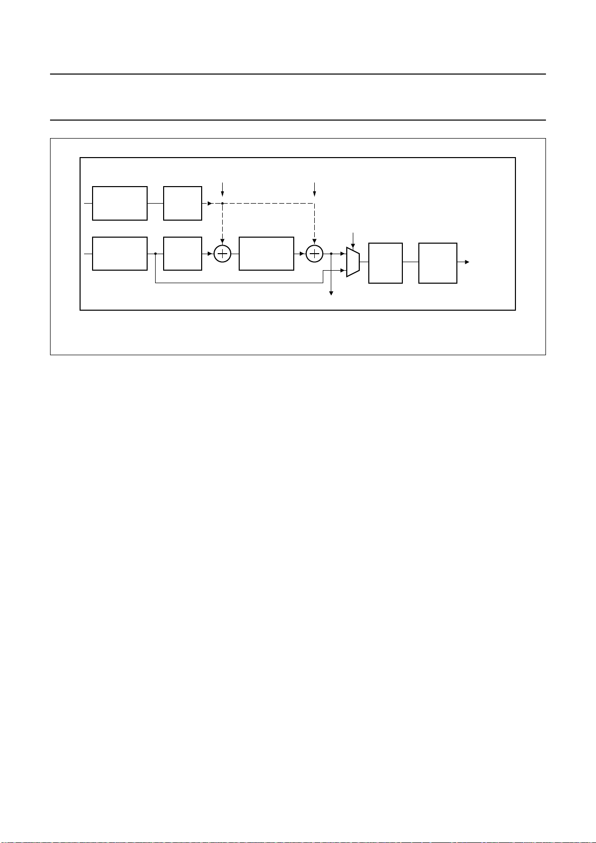
5 BLOCK DIAGRAM
6 PINNING
7 FUNCTIONAL DESCRIPTION
7.1 IC control
7.2 Microcontroller interface
7.3 Clock systems
7.4 IEC 60958 decoder
7.5 IEC 60958 encoder
7.6 Analog input
7.7 Analog output
7.8 Digital audio input and output
7.9 Power-on reset
8 APPLICATION MODES
8.1 Static mode pin assignment
8.2 Static mode basic applications
8.3 Microcontroller mode pin assignment
8.4 Microcontroller mode applications
9 SPDIF SIGNAL FORMAT
9.1 SPDIF channel encoding
9.2 SPDIF hierarchical layers
9.3 Timing characteristics
10 L3-BUS DESCRIPTION
10.1 Device addressing
10.2 Register addressing
10.3 Data write mode
10.4 Data read mode
11 I2C-BUS DESCRIPTION
11.1 Characteristics
11.2 Bit transfer
11.3 Byte transfer
11.4 Data transfer
11.5 Register address
11.6 Device address
11.7 Start and stop conditions
11.8 Acknowledgment
11.9 Write cycle
11.10 Read cycle
12 REGISTER MAPPING
12.1 Address mapping
12.2 Read/write registers mapping
12.3 Read registers mapping
13 LIMITING VALUES
14 THERMAL CHARACTERISTICS
15 CHARACTERISTICS
16 TIMING CHARACTERISTICS
17 PACKAGE OUTLINE
18 SOLDERING
18.1 Introduction to soldering surface mount
packages
18.2 Reflow soldering
18.3 Wave soldering
18.4 Manual soldering
18.5 Suitability of surface mount IC packages for
wave and reflow soldering methods
19 DATA SHEET STATUS
20 DEFINITIONS
21 DISCLAIMERS
22 PURCHASE OF PHILIPS I2C COMPONENTS
2003 Apr 10 2
Page 3

Philips Semiconductors Preliminary specification
Stereo audio codec with SPDIF interface UDA1355H
1 FEATURES
1.1 General
• 2.7 to 3.6 V power supply
• Integrated digitalinterpolator filter and Digital-to-Analog
Converter (DAC)
• 24-bit data path in interpolator
• No analog post filtering required for DAC
• Integrated Analog-to-Digital Converter (ADC),
Programmable Gain Amplifier (PGA) and digital
decimator filter
• 24-bit data path in decimator
• Master or slave mode for digital audio data I/O interface
• I2S-bus, MSB-justified, LSB-justified 16, 18, 20,
and 24 bits formats supported on digital I/O interface.
1.2 Control
• Controlled by means of static pins or microcontroller
(L3-bus or I2C-bus) interface.
1.3 IEC 60958 input
• On-chip amplifier for converting IEC 60958 input to
CMOS levels
• Supports level I, II and III timing
• Selectable IEC 60958 input channel, one of four
• Supports input frequencies from 28 to 96 kHz
• Lock indication signal available on pin LOCK
• 40 status bits can be read for left and right channel via
L3-bus or I2C-bus
• ChannelstatusbitsavailableviaL3-busorI2C-bus:lock,
pre-emphasis, audio sample frequency, two channel
Pulse Code Modulation (PCM) indication and clock
accuracy
• Pre-emphasis information of incoming IEC 60958
bitstream available in register
• Detection of digital data preamble, such as AC3,
available on pin in microcontroller mode.
1.4 IEC 60958 output
• 32, 44.1 and 48 kHz output frequencies (including
double and half of these frequencies) supported in
microcontroller mode
• Via microcontroller, 40 status bits can be set for left and
right channel.
1.5 Digital I/O interface
• Supports sampling frequencies from 16 to 100 kHz
• Supported static mode:
–I2S-bus format
– LSB-justified 16 and 24 bits format
– MSB-justified format.
• Supported microcontroller mode:
–I2S-bus format
– LSB-justified 16, 18, 20 or 24 bits format
– MSB-justified format.
• BCKand WS signals can be slave or master,depending
on application mode.
1.6 ADC digital sound processing
• Supports sampling frequencies from 16 to 100 kHz
• Analogfront-end includes a 0 to +24 dB PGA in steps of
3 dB, selectable via microcontroller interface
• Digital independent left and right volume control of
+24 to −63.5 dB in steps of 0.5 dB via microcontroller
interface
• Bitstream ADC operating at 64f
• Comb filter decreases sample rate from 64fsto 8f
• Decimator filter (8fsto fs) made of a cascade of three
FIR half-band filters.
s
s
• CMOS output level converted to IEC 60958 output
signal
• Full-swing digital signal, with level II timing using crystal
oscillator clock
• 32, 44.1 and 48 kHz output frequencies supported in
static mode
2003 Apr 10 3
1.7 DAC digital sound processing
• Digital de-emphasis for 32, 44.1, 48 and 96 kHz audio
sampling frequencies
• Automatic de-emphasis when using IEC 60958 to DAC
• Soft mute made of a cosine roll-off circuit selectable via
pin MUTE or L3-bus interface
Page 4

Philips Semiconductors Preliminary specification
Stereo audio codec with SPDIF interface UDA1355H
• Programmable digital silence detector
• Interpolating filter (fsto 64fs or fsto 128fs) comprising a
recursive and a FIR filter in cascade
• Selectable fifth-order noise shaper operating at 64fs or
third-order noise shaper operating at 128fs(specially for
low sampling frequencies, e.g. 16 kHz) generating
bitstream for DAC
• Filter Stream DAC (FSDAC)
• In microcontroller mode:
– Left and right volume control (for balance control)
0to−78 dB and −∞
– Left and right bass boost and treble control
– Optional resonant bass boost control
– Mixing possibility of two data streams.
2 GENERAL DESCRIPTION
The UDA1355H is a single-chip IEC 60958 decoder and
encoderwith integrated stereo digital-to-analogconverters
and analog-to-digital converters employing bitstream
conversion techniques.
The UDA1355H has a selectable one-of-four SPDIF input
(accepting level I, II and III timing) and one SPDIF output
which can generate level II output signals with CMOS
levels. In microcontroller mode the UDA1355H offers a
large variety of possibilities for defining signal flows
throughtheIC, offering a flexible analog, digital and SPDIF
converter chip with possibilities for off-chip sound
processing via the digital input and output interface.
A lock indicator is available on pin LOCK when the
IEC 60958 decoder and the clock regeneration
mechanism is in lock. By default the DAC output and the
digital data interface output are muted when the decoder
is not in lock.
TheUDA1355H contains two clock systems which can run
at independent frequencies, allowing to lock-on to an
incoming SPDIF or digital audio signal, and in the mean
time generating a stable signal by means of the crystal
oscillator for driving, for example, the ADC or SPDIF
output signal.
Using the crystal oscillator (which requires a 12.288 MHz
crystal) and the on-chip low jitter PLL, all standard audio
sampling frequencies (fs= 32, 44.1 and 48 kHz including
half and double these frequencies) can be generated.
3 ORDERING INFORMATION
TYPE
NUMBER
UDA1355H QFP44 plastic quad flat package; 44 leads (lead length 1.3 mm); body
NAME DESCRIPTION VERSION
10 × 10 × 1.75 mm
PACKAGE
SOT307-2
2003 Apr 10 4
Page 5
Philips Semiconductors Preliminary specification
Stereo audio codec with SPDIF interface UDA1355H
4 QUICK REFERENCE DATA
SYMBOL PARAMETER CONDITIONS MIN. TYP. MAX. UNIT
Supplies
V
DDA1
V
DDA2
V
DDX
V
DDI
V
DDE
I
DDA1
I
DDA2
I
DDX
I
DDI
I
DDE
T
amb
Digital-to-analog converter; fi= 1 kHz; V
V
o(rms)
∆V
o
(THD+N)/S total harmonic
S/N signal-to-noise ratio IEC 60958 input; code = 0;
α
cs
DAC supply voltage 2.7 3.0 3.6 V
ADC supply voltage 2.7 3.0 3.6 V
crystal oscillator and PLL
2.7 3.0 3.6 V
supply voltage
digital core supply voltage 2.7 3.0 3.6 V
digital pad supply voltage 2.7 3.0 3.6 V
DAC supply current fs= 48 kHz; power-on − 4.7 − mA
f
= 96 kHz; power-on − 4.7 − mA
s
f
= 48 kHz; power-down − 1.7 −µA
s
= 96 kHz; power-down − 1.7 −µA
f
s
ADC supply current fs= 48 kHz; power-on − 10.2 − mA
f
= 96 kHz; power-on − 10.4 − mA
s
f
= 48 kHz; power-down − 0.2 −µA
s
= 96 kHz; power-down − 0.2 −µA
f
s
crystal oscillator and PLL
supply current
fs= 48 kHz; power-on − 0.9 − mA
f
= 96 kHz; power-on − 1.2 − mA
s
digital core supply current fs= 48 kHz; all on − 18.2 − mA
f
= 96 kHz; all on − 34.7 − mA
s
digital pad supply current fs= 48 kHz; all on − 0.5 − mA
f
= 96 kHz; all on − 0.7 − mA
s
ambient temperature −40 − +85 °C
= 3.0 V
DDA1
output voltage (RMS
− 900 − mV
value)
output voltage unbalance − 0.1 − dB
distortion-plus-noise to
signal ratio
IEC 60958 input; f
at 0 dB −−88 − dB
at −20 dB −−75 − dB
=48kHz
s
at −60 dB; A-weighted −−37 − dB
IEC 60958 input; fs=96kHz
at 0 dB −−83 − dB
at −60 dB; A-weighted −−37 − dB
A-weighted
fs= 48 kHz − 98 − dB
f
= 96 kHz − 96 − dB
s
channel separation − 100 − dB
2003 Apr 10 5
Page 6
Philips Semiconductors Preliminary specification
Stereo audio codec with SPDIF interface UDA1355H
SYMBOL PARAMETER CONDITIONS MIN. TYP. MAX. UNIT
Analog-to-digital converter; fi= 1 kHz; V
(rms) input voltage (RMS value) Vo= −1.16 dBFS digital output − 1.0 − V
V
i
∆V
i
input voltage unbalance − 0.1 − dB
(THD+N)/S total harmonic
distortion-plus-noise to
signal ratio
= 3.0 V
DDA2
f
= 48 kHz
s
at 0 dB −−85 − dB
at −60 dB; A-weighted −−35 − dB
f
= 96 kHz
s
at 0 dB −−85 − dB
at −60 dB; A-weighted −−35 − dB
S/N signal-to-noise ratio code = 0; A-weighted
f
= 48 kHz − 97 − dB
s
f
= 96 kHz − 95 − dB
s
α
cs
channel separation − 100 − dB
External crystal
f
C
xtal
L(xtal)
crystal frequency − 12.288 − MHz
crystal load capacitor − 10 − pF
Device reset
t
rst
reset time − 250 −µs
Power consumption
P
tot
total power consumption IEC 60958 input; fs=48kHz
DAC in playback mode − 74 − mW
DAC in Power-down mode − 63 − mW
2003 Apr 10 6
Page 7
Philips Semiconductors Preliminary specification
Stereo audio codec with SPDIF interface UDA1355H
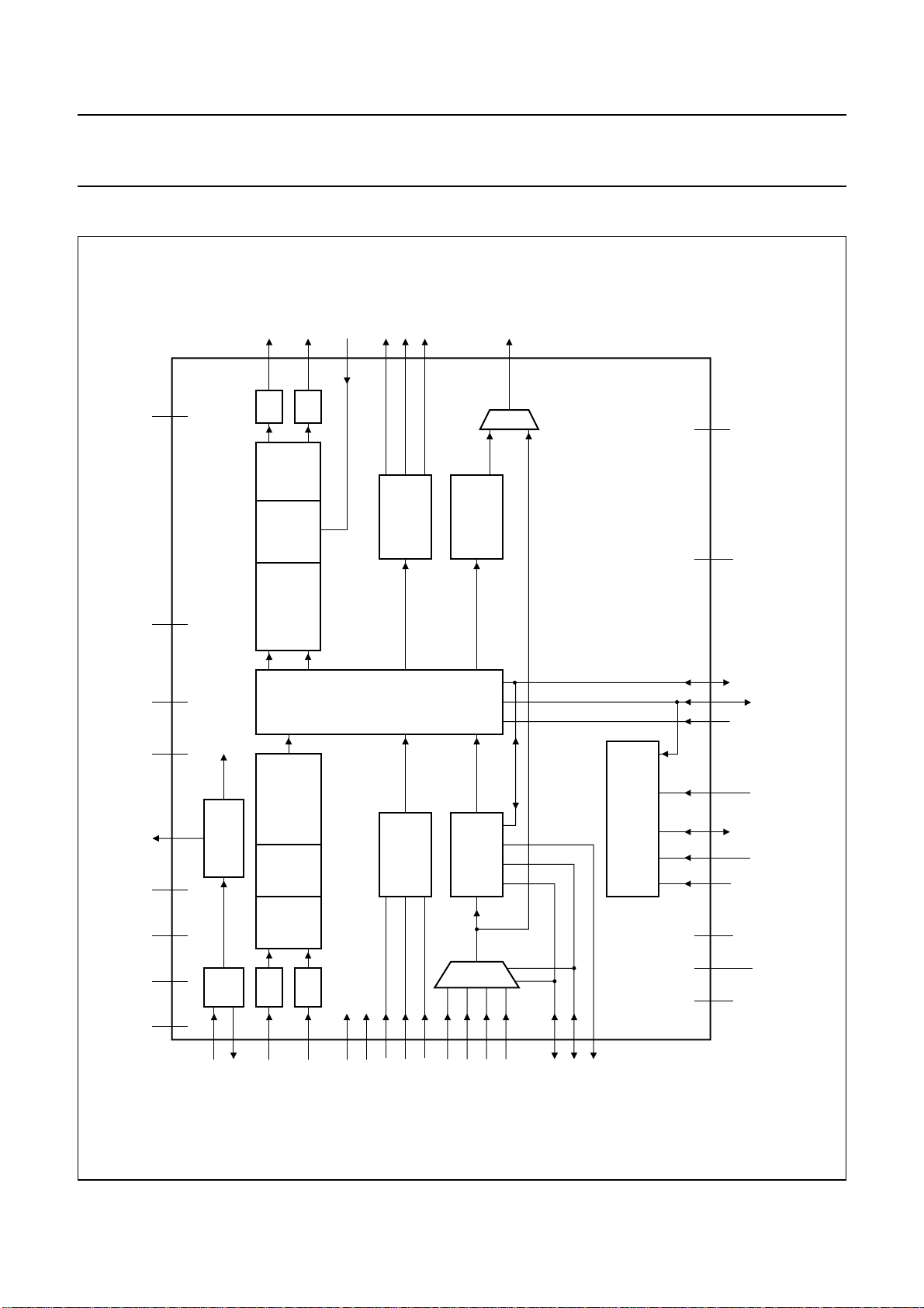
5 BLOCK DIAGRAM
VOUTL
VOUTR
MUTE
WSO
DATAO
DDA1
V
40
DAC
NOISE
INTER-
42
DAC
SHAPER
POLATOR
BCKO
9
44
8
10
DATA OUT
5
IEC 60958
ENCODER
SPDIFOUT
UDA1355H
41
MGU826
V
V
SSA1
SSE
DDE
V
ndbook, full pagewidth
REF
V
DDI
V
CLK_OUT
DDA2
V
ADCP
V
SSX
V
DDX
V
32 37 27 38 6 3911
15
12
TIMING
CLOCK AND
XTAL
13
14
AUDIO
AUDIO
ADC
34
FEATURE
PROCESSOR
FEATURE
PROCESSOR
DECI-
MATOR
COMB
FILTER
ADC
36
INPUT
16432
AND
OUTPUT
SELECT
DATA IN
3
1
IEC 60958
SLICER
232425
DECODER
26
21224
CONTROL
INTERFACE
MODE2
MODE1
MODE0
Fig.1 Block diagram.
SEL_STATIC
MP2
MP0
SSIS
V
ADCN
V
MP1
SSA2
V
29 30 31 20 17 18 19 7
33 35 28
This text is here in white to force landscape pages to be rotated correctly when browsing through the pdf in the Acrobat reader.This text is here in
_white to force landscape pages to be rotated correctly when browsing through the pdf in the Acrobat reader.This text is here inThis text is here in
white to force landscape pages to be rotated correctly when browsing through the pdf in the Acrobat reader. white to force landscape pages to be ...
2003 Apr 10 7
XTALIN
XTALOUT
VINL
VINR
RTCB
RESET
WSI
BCKI
DATAI
SPDIF0
SPDIF1
SPDIF2
SPDIF3
LOCK
SLICER_SEL0
SLICER_SEL1
Page 8
Philips Semiconductors Preliminary specification
Stereo audio codec with SPDIF interface UDA1355H
6 PINNING
SYMBOL PIN PAD
(1)
DESCRIPTION
BCKI 1 bpt4mtht5v bit clock input (master or slave)
WSI 2 bpt4mtht5v word select input (master or slave)
DATAI 3 iptht5v digital data input
LOCK 4 op4mc PLL lock indicator output
SPDIFOUT 5 op4mc SPDIF output
V
V
DDE
SSE
6 vdde digital pad supply voltage
7 vsse digital pad ground
DATAO 8 ops5c digital data output
WSO 9 bpt4mtht5v word select output (master or slave)
BCKO 10 bpt4mtht5v bit clock output (master or slave)
CLK_OUT 11 op4mc clock output; 256f
V
DDX
12 vddco crystal oscillator and PLL supply voltage
or 384f
s
s
XTALIN 13 apio crystal oscillator input
XTALOUT 14 apio crystal oscillator output
V
SSX
15 vssco crystal oscillator and PLL ground
RESET 16 ipthdt5v reset input
MODE0 17 apio mode selection input 0 for static mode or microcontroller mode (grounded
2
for I
C-bus)
MODE1 18 bpts5tht5v mode selection input 1 for static mode or AO address input and output for
microcontroller mode
MODE2 19 bpts5tht5v mode selection input 2 for static mode or U_RDY output for microcontroller
mode
SEL_STATIC 20 apio selection input for static mode, I
2
C-bus mode or L3-bus mode
SLICER_SEL0 21 bpts5tht5v SPDIF slicer selection input 0 for static mode and USER bit output for
microcontroller mode
SLICER_SEL1 22 bpts5tht5v SPDIF slicer selection input 1 for static mode and AC3 preamble detect
output for microcontroller mode
SPDIF0 23 apio SPDIF input 0
SPDIF1 24 apio SPDIF input 1
SPDIF2 25 apio SPDIF input 2
SPDIF3 26 apio SPDIF input 3
V
V
DDI
SSIS
27 vddi digital core supply voltage
28 vssis digital core ground
MP0 29 apio multi-purpose pin 0: frequency select for static mode, not used for
microcontroller mode
MP1 30 iptht5v multi-purpose pin 1: SFOR1 for static mode, SCL for I2C-bus mode and
L3CLOCK for L3-bus mode
2
MP2 31 iic400kt5v multi-purpose pin 2: SFOR0 for static mode, SDA for I
C-bus mode and
L3DATA for L3-bus mode
V
ADCP
V
ADCN
32 vddco positive ADC reference voltage
33 vssco negative ADC reference voltage
2003 Apr 10 8
Page 9
Philips Semiconductors Preliminary specification
Stereo audio codec with SPDIF interface UDA1355H
SYMBOL PIN PAD
(1)
DESCRIPTION
VINL 34 apio ADC left channel input
V
SSA2
35 vssco ADC ground
VINR 36 apio ADC right channel input
V
V
V
DDA2
REF
DDA1
37 vddco ADC supply voltage
38 apio reference voltage for ADC and DAC
39 vddco DAC supply voltage
VOUTL 40 apio DAC left channel output
V
SSA1
41 vssco DAC ground
VOUTR 42 apio DAC right channel output
RTCB 43 ipthdt5v test control input
MUTE 44 iipthdt5v DAC mute input
Note
1. See Table 1.
Table 1 Pad description
PAD DESCRIPTION
iptht5v input pad; push-pull; TTL with hysteresis; 5 V tolerant
ipthdt5v input pad; push-pull; TTL with hysteresis; pull-down; 5 V tolerant
op4mc output pad; push-pull; 4 mA output drive; CMOS
ops5c output pad; push-pull; 5 ns slew rate control; CMOS
bpt4mtht5v bidirectional pad; push-pull input; 3-state output; 4 mA output drive; TTL with hysteresis;
5 V tolerant
bpts5tht5v bidirectional pad; push-pull input; 3-state output; 5 ns slew rate control; TTL with hysteresis;
5 V tolerant
iic400kt5v I
2
C-bus pad; 400 kHz I2C-bus specification with open drain; 5 V tolerant
apio analog pad; analog input or output
vddco analog supply pad
vssco analog ground pad
vdde digital supply pad
vsse digital ground pad
vddi digital core supply pad
vssis digital core ground pad
2003 Apr 10 9
Page 10
Philips Semiconductors Preliminary specification
Stereo audio codec with SPDIF interface UDA1355H
handbook, full pagewidth
DDA1
REF
V
38
DDA2
V
37
VINR
36
SSA2
V
35
VINL
34
33
32
31
30
29
28
27
26
25
24
23
V
ADCN
V
ADCP
MP2
MP1
MP0
V
SSIS
V
DDI
SPDIF3
SPDIF2
SPDIF1
SPDIF0
BCKI
WSI
DATAI
LOCK
SPDIFOUT
V
DDE
V
SSE
DATAO
WSO
BCKO
CLK_OUT
RTCB
43
42
V
VOUTL
41
40
UDA1355H
V
39
MUTE
44
1
2
3
4
5
6
7
8
9
10
11
SSA1
VOUTR
12
13
14
15
XTALIN
XTALOUT
SSX
V
DDX
V
Fig.2 Pin configuration.
7 FUNCTIONAL DESCRIPTION
7.1 IC control
The UDA1355H can be controlled either via static pins or
via the microcontroller serial hardware interface being the
I2C-bus with a clock up to 400 kHz or the L3-bus with a
clock up to 2 MHz. It is recommended to use the
microcontroller interface since this gives full access to all
the IC features.
The two microcontroller interfaces only differ in interface
format. The register addresses and features that can be
controlled are identical for L3-bus mode and I2C-bus
mode.
The UDA1355H can operate in three control modes:
• Static mode with limited features
• L3-bus mode with full featuring
• I2C-bus mode with full featuring.
The modes are selected via the 3-level pin SEL_STATIC
according to Table 2.
21
16
17
RESET
MODE0
18
19
MODE2
MODE1
22
20
SEL_STATIC
SLICER_SEL1
SLICER_SEL0
MGU828
Table 2 Control mode selection via pin SEL_STATIC
LEVEL MODE
HIGH static mode
MID I2C-bus mode
LOW L3-bus mode
7.2 Microcontroller interface
The UDA1355H has a microcontroller interface and all the
sound processing features and system settings can be
controlled by the microcontroller.
The controllable settings are:
• Restoring L3-bus defaults
• Power-on settings for all blocks
• Digital interface input and output formats
• Volume settings for the decimator
• PGA gain settings
2003 Apr 10 10
Page 11
Philips Semiconductors Preliminary specification
Stereo audio codec with SPDIF interface UDA1355H
• Set two times 40 bits of channel status bits of the SPDIF
output
• Select one of four SPDIF input sources
• Enable digital mixer inside interpolator
• Control mute and mixer volumes of digital mixer
• Selection of filter mode and settings of treble and bass
boost for the interpolator (DAC) section
• Volume settings of interpolator
• Selectionof soft mute via cosine roll-off (only effectivein
L3-bus control mode) and bypass of auto mute
• Selection of de-emphasis
• Enable and control of digital mixer inside interpolator.
The readable settings are:
• Mute status of interpolator
• PLL lock and adaptive lock
• Two times 40 bits of channels status bits of the SPDIF
input signal.
7.3 Clock systems
The UDA1355H has two clock systems.
The first system uses an external crystal of 12.288 MHz to
generate the audio related system clocks. Only a crystal
with a frequency of 12.288 MHz is allowed.
The second system is a PLL which locks on the SPDIF or
incoming digital audio signal (e.g. I2S-bus) and recovers
the system clock.
7.3.1 CRYSTAL OSCILLATOR CLOCK SYSTEM
The crystal oscillator and the on-chip PLL and divider
circuit can be used to generate internal and external clock
signals related to standard audio sampling frequencies
(such as 32, 44.1 and 48 kHz including half and double of
these frequencies).
The audio frequencies supported in either microcontroller
mode or static mode are given in Table 3.
Table 3 Output frequencies
OUTPUT FREQUENCY
BASIC AUDIO
FREQUENCY
32 kHz 256 × 16 kHz
44.1 kHz 256 × 22.05 kHz
48 kHz 256 × 24 kHz
Remarks:
• If an application mode is selected which does not need
a crystal oscillator, the crystal oscillator cannot be
omitted. The reason is that the interpolator switches to
the crystal clock when an SPDIF input signal is
removed. This switch prevents the noise shaper noise
from moving inside the audio band as the PLL gradually
decreases in frequency.
• If no accurate output frequency is needed, the crystal
can be replaced with a resonator.
• Instead of the crystal, a 12.288 MHz system clock can
be applied to pin XTALIN.
MICRO-
CONTROLLER
MODE
384 × 16 kHz
256 × 32 kHz 256 × 32 kHz
384 × 32 kHz
256 × 64 kHz
384 × 64 kHz
384 × 22.05 kHz
256 × 44.1 kHz 256 × 44.1 kHz
384 × 44.1 kHz
256 × 88.2 kHz
384 × 88.2 kHz
384 × 24 kHz
256 × 48 kHz 256 × 48 kHz
384 × 48 kHz
256 × 96 kHz
384 × 96 kHz
STATIC MODE
2003 Apr 10 11
The block diagram of the crystal oscillator and the PLL
circuit is given in Fig.3.
Page 12
Philips Semiconductors Preliminary specification
Stereo audio codec with SPDIF interface UDA1355H
7.3.4 CLOCK OUTPUT
handbook, halfpage
12.288 MHz
XTALIN
XTALOUT
CLK_OUT
13
CRYSTAL
14
OSCILLATOR
11
L3-bus or I
register setting
256fs or 384fs clock
PLL clock
2
C-bus
UDA1355H
PLL
MODULE
MGU830
Fig.3 Crystal oscillator clock system.
7.3.2 PLL CLOCK SYSTEM
The PLL locks on the incoming digital data of the SPDIF or
WS input signal. The PLL recovers the clock from the
SPDIForWSI signal and removes jitter toproduceastable
system clock (see Fig.4).
The UDA1355H has a clock output pin (pin CLK_OUT),
which can be used to drive other audio devices in the
system. In microcontroller mode the output clock is
256fsor 384fs. In static mode the output clock is 256 times
32, 44.1 and 48 kHz.
The source of the output clock is either the crystal
oscillator or the PLL, depending on the selected
application and control mode.
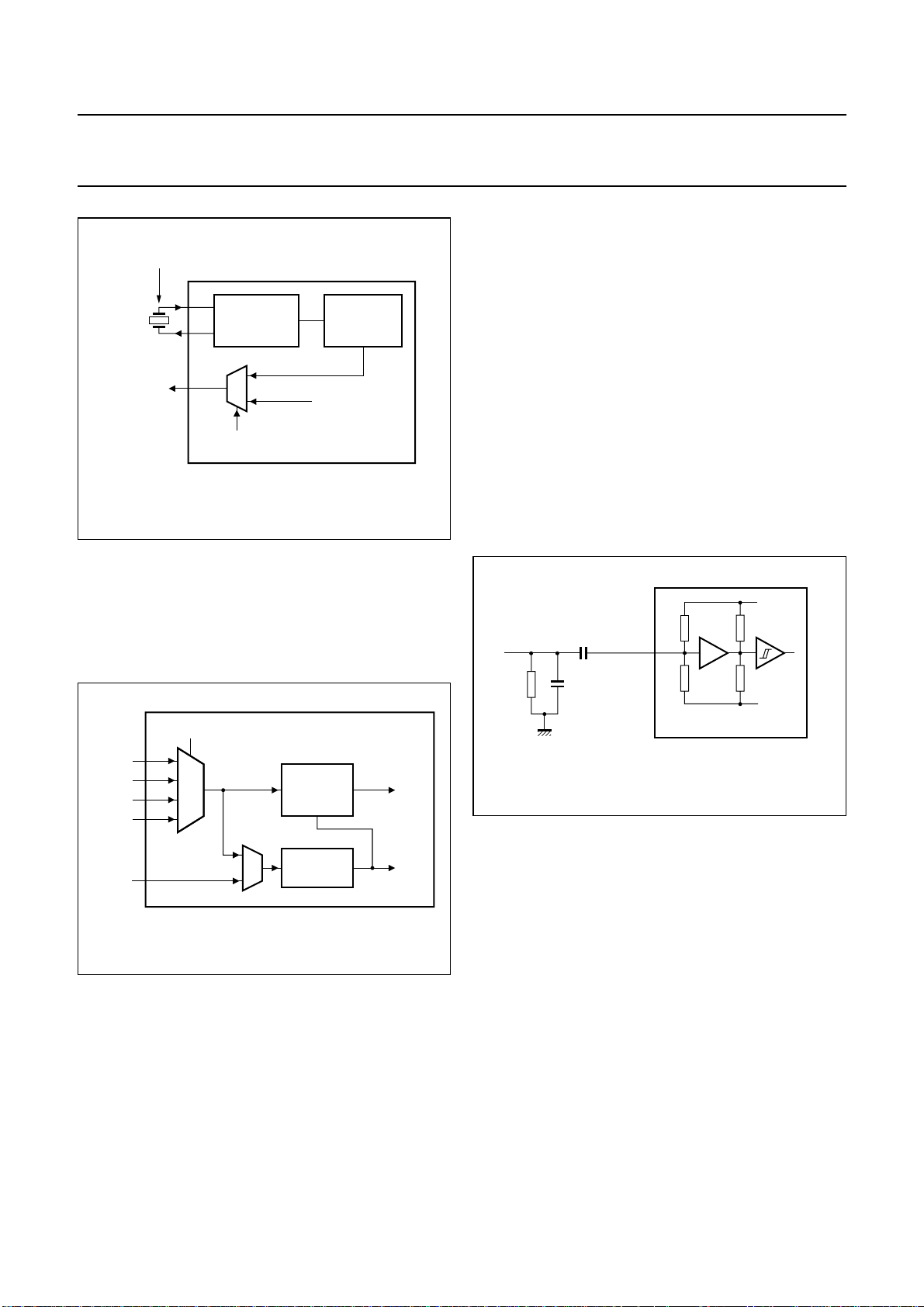
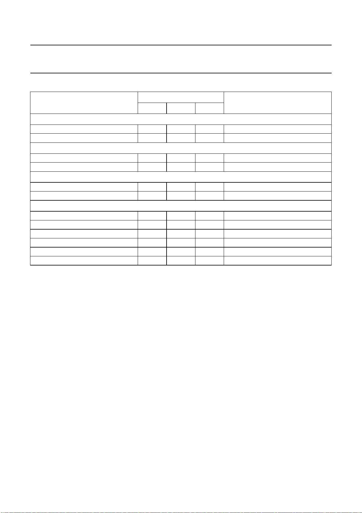
7.4 IEC 60958 decoder
The UDA1355H IEC 60958 decoder can selectone of four
SPDIFinputchannels. An on-chip amplifier with hysteresis
amplifies the SPDIF input signal to CMOS level, making it
possible to accept both analog and digital SPDIF signals
(see Fig.5).
handbook, halfpage
23
24
25
26
75 Ω
10 nF
180 pF
SPDIF0
SPDIF1
SPDIF2
SPDIF3
SPDIF0
SPDIF1
SPDIF2
SPDIF3
WSI
select SPDIF source
23
24
25
26
SLICER
2
IEC 60958
DECODER
PLL
UDA1355H
256f
384f
s
or
s
MGU827
Fig.4 PLL clock system.
7.3.3 WORD SELECTION DETECTION CIRCUIT
This circuit is clocked by the 12.288 MHz crystal oscillator
clock and generates a Word Selection (WS) detection
signal. If the WS detector does not detect any WS edge,
defined as 7 times LOW and 7 times HIGH, then the
WS detection signal is LOW. This information can be used
tosetthe clock for the noise shaper in theinterpolator.This
will prevent noise shaper noise in the audio band.
UDA1355H
MGU829
Fig.5 IEC 60958 input circuit.
7.4.1 AUDIO DATA
From the incoming SPDIF bitstream 24 bits of data for the
left and right channel are extracted.
There is a hard mute (not a cosine roll-off mute) if the
IEC 60958 decoder is out of lock or detects bi-mark phase
encoding violations. The lock indicator and the key
channel status bits are accessible in L3-bus mode.
The UDA1355H supports the following sample
frequencies and data rates, including half and double of
these frequencies:
• fs= 32 kHz; resulting in a data rate of 2.048 Mbit/s
• fs= 44.1 kHz; resulting in a data rate of 2.8224 Mbit/s
• fs= 48 kHz; resulting in a data rate of 3.072 Mbit/s.
2003 Apr 10 12
Page 13
Philips Semiconductors Preliminary specification
Stereo audio codec with SPDIF interface UDA1355H
7.4.2 CHANNEL STATUS AND USER BITS
As well as the data bits there are several IEC 60958 key
channel status bits:
• Pre-emphasis and audio sampling frequency bits
• Two channel PCM indicator bits
• Clock accuracy bits.
In total 40 status bits per channel are recovered from the
incomingIEC 60958bitstream.Thesearereadableviathe
microcontroller interface.
User bits, which can contain a large variety of data, such
asCD text, are output to pin SLICER_SEL0 (see Table 4).
In microcontroller mode this signal contains the raw user
bits extracted from the SPDIF bitstream. Signal U_RDY
gives a pulse on pin MODE2 each time there is a new user
bit available. Both signals can be used by an external
microcontroller to grab and decode the user bits.
Table 4 Signal names in microcontroller mode
PIN NAME SIGNAL NAME
SLICER_SEL0 USER
MODE2 U_RDY
SLICER_SEL1 AC3
7.4.3 D
Audio and digital data can be transmitted in the SPDIF
bitstream. The PCM channel status bit should be set to
logic 1 if the SPDIF bitstream is carrying digital data
instead of audio data, but in practice it proves that not all
equipment handles these channel status bits properly.
In the UDA1355H, digital data is detected via bit PCM, or
via the sync bytes as specified by IEC. These sync bytes
are two sync words, F872H and 4E1FH (two subframes)
preceded by four or more subframes filled with zeros.
Signal AC3 is kept HIGH for 4096 frames when the
UDA1355H detects this burst preamble. Signal AC3 is
present on pin SLICER_SEL1 in microcontroller mode
(see Table 4).
IGITAL DATA
7.5 IEC 60958 encoder
When using the crystal oscillator clock, the IEC 60958
encoder output is a full-swing digital signal with level II
timing.
When the recovered clock from the PLL is used the
IEC 60958 encoder will function correctly but will not meet
level II timing requirements.
7.5.1 S
All user and channel status bits are set to logic 0. This is
default value specified by IEC.
In static mode 0 and 2, the selected SPDIF input channel
can be looped through to pin SPDIFOUT (see Fig.6).
7.5.2 MICROCONTROLLER MODE
Two times 40 channel status bits can be set. Default value
for each status bit is logic 0. When setting the channel
status bits, it is possible to set only the left channel status
bits and have the bits copied to the right channel.
The procedure of writing the channel status bits is as
follows:
1. Set bit SPDO_VALID = 0 to prevent immediately
2. Set bit l_r_copy = 1 if the right channel needs the
3. Write the left and right channel status bits.
4. Set bit SPDO_VALID = 1 after writing all channel
In microcontroller modes 2 and 13, the selected SPDIF
input channel can be looped through to pin SPDIFOUT
(see Fig.6).
TATIC MODE
sending the status bits during writing.
same status bits as the left channel or set
bit l_r_copy = 0 if the right channel needs different
status bits to the left channel.
statusbitstotheregister.StartingfromthenextSPDIF
block the IEC 60958 encoder will use the new status
bits.
2003 Apr 10 13
Page 14
Philips Semiconductors Preliminary specification
Stereo audio codec with SPDIF interface UDA1355H
handbook, full pagewidth
SPDIF0
SPDIF1
SPDIF2
SPDIF3
SPDOUT_SEL1
SPDOUT_SEL0
23
24
25
26
SLICER_SEL[1:0
SLICER
select
SPDIF source
21, 22
]
SPDIF
source
UDA1355H
IEC 60958
DECODER
IEC 60958
ENCODER
Fig.6 Selection options for SPDIF output.
7.6 Analog input
7.6.1 ADC
The analog input is equipped with a Programmable Gain
Amplifier (PGA) which can be controlled via the
microcontroller interface. The control range is from
0 to 24 dB gain in 3 dB steps independent for the left and
right channels.
In applications in with a 2 V (RMS) input signal, a 12 kΩ
resistor must be used in series with the input of the ADC.
The 12 kΩ resistor forms a voltage divider together with
the internal ADC resistor and ensures that the voltage,
applied to the input of the IC, never exceeds 1 V (RMS).
In the application for a 2 V (RMS) input signal, the PGA
must be set to 0 dB. When a 1 V (RMS) input signal is
applied to the ADC in the same application, the PGA gain
must be set to 6 dB.
An overview of the maximum input voltages allowed with
and without an external resistor and the PGA gain setting
is given in Table 5.
Table 5 Maximum input voltage; VDD=3V
EXTERNAL
RESISTOR
(12 kΩ)
PGA GAIN
SETTING
MAXIMUM
INPUT
VOLTAGE
Present 0 dB 2 V (RMS)
6 dB 1 V (RMS)
Absent 0 dB 1 V (RMS)
6 dB 0.5 V (RMS)
SPDOUT_SEL2
MODE[3:0
17 to 19 20
MODE[2:0]SEL_STATIC
]
5
SPDIF OUT
MGU833
7.6.2 DECIMATION
Thedecimation from 64fsisperformed in two stages: comb
filter and decimation filter. The first stage realizes a
fourth-order characteristic with a decimation factor
sin x
----------- x
of eight. The second stage consists of three half-band
filters each decimating by a factor of two. Table 6 shows
the characteristics.
Table 6 Decimation filter characteristics
ITEM CONDITIONS VALUE (dB)
Pass-band ripple 0 to 0.45f
Stop band >0.55f
Dynamic range 0 to 0.45f
Overallgain from ADC
input to digital output
DC; V
note 1
= 0 dB;
I
s
s
s
±0.02
−60
140
−1.16
Note
1. Theoutput is not 0 dB when V
=1VatVDD=3V.
I(rms)
This is because the analog components can spread
over the process. When there is no external resistor,
the −1.16 dB scaling prevents clipping caused by
process mismatch.
In the ADC path there are left and right independent digital
volume controls with a range from +24 to −63.5 dB
and −∞ dB. This volume control is also used as a digital
linear mute that can be used to prevent plops when
powering-up or powering down the ADC front path.
2003 Apr 10 14
Page 15

Philips Semiconductors Preliminary specification
Stereo audio codec with SPDIF interface UDA1355H
7.6.3 DC FILTERING
In the decimator there are two digital DC blocking circuits.
The first blocking circuit is in front of the volume control to
remove DC bias from the ADC output. The DC bias is
added in the ADC to prevent audio band Idle tones
occurring in the noise shaper. With the DC components
removed, a signal gain of 24 dB can be achieved.
The second blocking circuit removes the DC components
introduced by the decimator stage.
7.6.4 OVERLOAD DETECTION
Bit OVERFLOW = 1 when the output data in the left or
right channel is larger than −1.16 dB of the maximum
possible digital swing. This condition is set for at least
512fs cycles (that is 11.6 ms at fs= 44.1 kHz). This
time-out is reset for each infringement.
7.7 Analog output
7.7.1 AUDIO FEATURE PROCESSOR
The audio feature processor provides automatic
de-emphasis for the IEC 60958 bitstream.
In microcontroller mode all features are available and
there is a default mute on start up.
7.7.2 INTERPOLATING FILTER
The digital filter interpolates from 1fsto 64fs, or from
1fsto 128fs, by cascading a half-band filter and a FIR filter.
The stereo interpolator has the following basic features:
• 24-bit data path
• Mixing of two channels:
– To prevent clipping inside the core, there is an
automatic signal level correction of −6 dB scaling
before mixing and +6 dB gain after digital volume
control
– Position of mixing can be set before or after bass
boost and treble
– Mastervolume control andmutewithindependent left
and right channel settings for balance control
– Independently left and right channel de-emphasis,
volume control and mute (no left or right)
– Output of the mixer is to the I2S-bus or IEC 60958
decoder.
• Full FIR filter implementation for all the upsampling
filters
• Integrated digital silence detection for left and right
channels with selectable silence detection time
• Support for 1fsand 2fs input data rate and 192 kHz
audio via I2S-bus.
The stereo interpolator has the following sound features:
• Linear volume control using 14-bit coefficients with
0.25 dB steps: range 0 to −78 dB and −∞ dB; hold for
master volume and mixing volume control
• A cosine roll-off soft mute with 32 coefficients; each
coefficientis used for four samples, in total 128 samples
are needed to fully mute or de-mute (approximately
3 ms at fs= 44.1 kHz)
• Independent selectable de-emphasis for 32, 44.1, 48
and 96 kHz for both channels
• Treble is the selectable positive gain for high
frequencies. The edge frequency of the treble is fixed
and depends on the sampling frequency. Treble can be
set independently for left and right channel with two
settings:
–fc= 1.5 kHz; fs= 44.1 kHz; 0 to 6 dB gain range with
2 dB steps
–fc= 3 kHz; fs= 44.1 kHz; 0 to 6 dB gain range with
2 dB steps.
• Normal bass boost is the selectable positive gain for low
frequencies. The edge frequency of the bass boost is
fixed and depends on the sampling frequency. Normal
bassboostcan be set independently for the left and right
channel with two sets:
–fc= 250 Hz;fs= 44.1 kHz;0 to 18 dBgainrangewith
2 dB steps
–fc= 300 Hz;fs= 44.1 kHz;0 to 24 dBgainrangewith
2 dB steps.
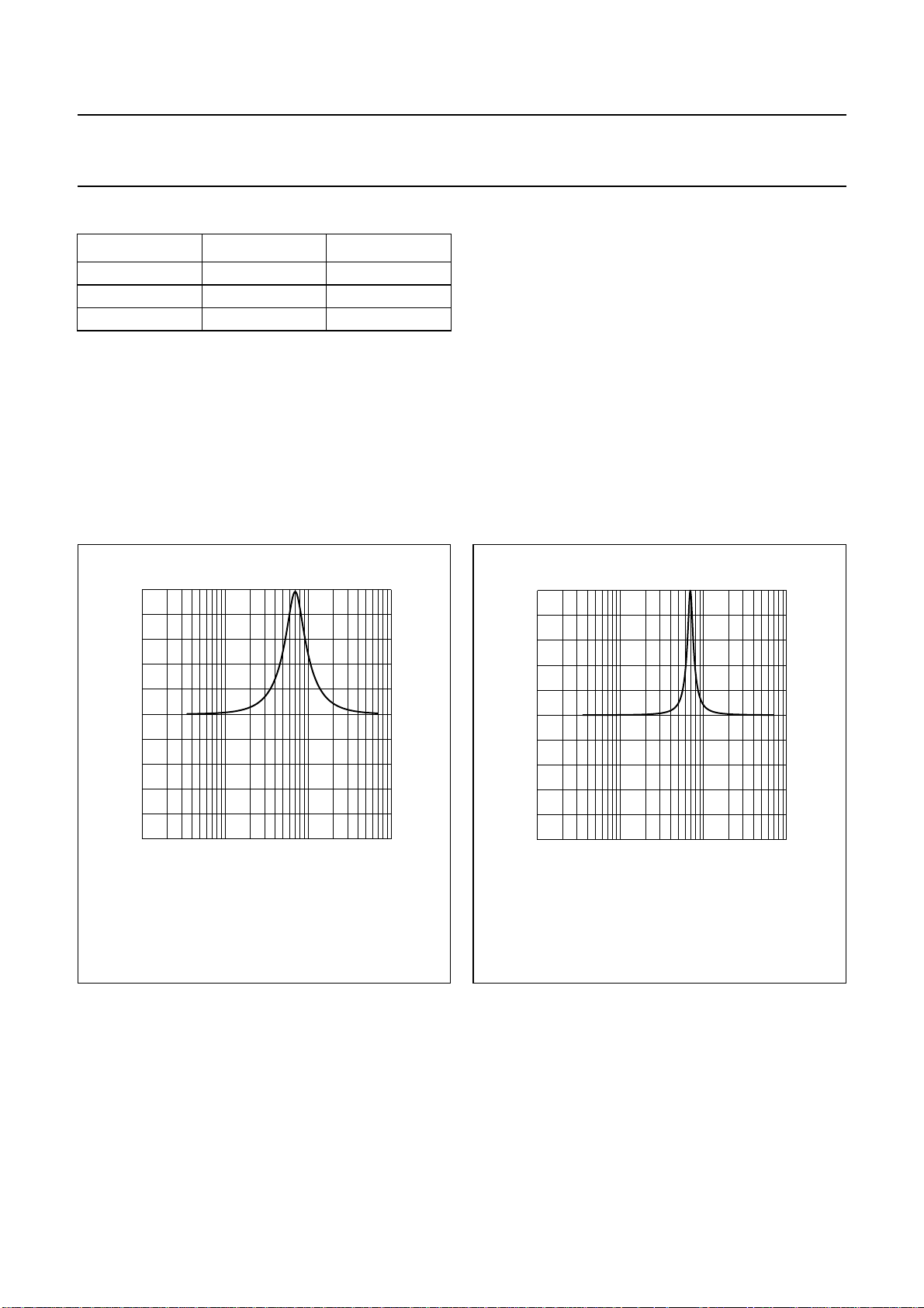
• Resonant bass boost optional function is selected if
bit BASS_SEL = 1. When selected, the characteristics
aredeterminedbysix14-bitcoefficients.Resonantbass
boost controls the left and right channel with the same
characteristics. When resonant bass boost is selected,
the treble control also changes to a single control for
both channels following the gain setting of the left
channel.
Asoftware program is available foruserstogenerate the
required six 14-bit coefficients by entering the desired
centre frequency (fc), positive or negative peak gain,
sampling frequency (fs) and shape factor (see
Figs 7 and 8).
2003 Apr 10 15
Page 16
Philips Semiconductors Preliminary specification
Stereo audio codec with SPDIF interface UDA1355H
Table 7 Interpolation filter characteristics
ITEM CONDITIONS VALUE (dB)
Pass-band ripple 0 to 0.45f
Stop band >0.55f
Dynamic range 0 to 0.4535f
7.7.3 D
IGITAL MIXER
s
s
s
±0.035
−60
140
The UDA1355H has a digital mixer inside the interpolator.
Thedigitalmixer can be used as a cross over or a selector.
A functional block diagram of the mixer mode is shown in
Fig.9. This mixer can be used in microcontroller mode
only.
The UDA1355H can be set to the mixer mode by setting
bit MIX = 1.In the mixer mode, there are three volume and
10
handbook, halfpage
gain
8
(dB)
6
4
2
0
−2
−4
−6
−8
−10
11010
MGU832
2103
f (Hz))
mute controls available: for source 1, for source 2 and for
the master (sum) signal. All three volume ranges can be
controlled in 0.25 dB steps.
Topreventclipping inside the mixer, the signals are scaled
with −6 dB before mixing, therefore the sum of the two
signals is always equal to or lower than 0 dB. After the
mixing there is a 6 dB gain in the master volume control.
This means that at the analog output the signal can clip,
but the clipping can be undone by decreasing the master
volume control.
2
The output of the mixer is available via the I
S-bus output
or via the SPDIF output. The output signal of the mixer is
scaled to a maximum of 0 dB, so the digital output can
never clip.
10
handbook, halfpage
gain
8
(dB)
6
4
2
0
−2
−4
−6
−8
−10
11010
MGU831
2103
f (Hz))
fc=70Hz
fs= 44.1 kHz
Peak gain = 10 dB
Shape factor = 1.4142
Fig.7 Resonant bass boost example 1.
2003 Apr 10 16
fc=70Hz
fs= 44.1 kHz
Peak gain = 10 dB
Shape factor = 1.4142
Fig.8 Resonant bass boost example 2.
Page 17
Philips Semiconductors Preliminary specification
Stereo audio codec with SPDIF interface UDA1355H
handbook, full pagewidth
channel 2
VOLUME
DE-EMPHASIS
VOLUME
DE-EMPHASIS
channel 1
AND
MUTE
AND
MUTE
mixing before
sound features
BASS-BOOST
AND
TREBLE
Fig.9 Digital mixer (DAC) inside the interpolator DSP.
7.7.4 DIGITAL SILENCE DETECTOR
The UDA1355H is equipped with adigital silence detector.
This detects whether a certain amount of consecutive
samples are 0. The number of samples can be set with
bits SD_VALUE[1:0] to 3200, 4800, 9600 or 19600
samples.
The digital silence detection status can be read via the
microcontroller interface.
7.7.5 NOISE SHAPER (DAC)
The noise shaper shifts in-band quantization noise to
frequencies above the audio band. The noise shaper
output is converted into an analog signal using a Filter
Stream Digital-to-Analog Converter (FSDAC). This noise
shaping technique enables high signal-to-noise ratios to
be achieved.
The UDA1355H is equipped with two noise shapers:
• A third-order noise shaper operating at 128fs. Which is
used at low sampling frequencies (8 to 16 kHz) to
prevent noise shaper noise shifting into the audio band
for the fifth-order noise shaper
• A fifth-order noise shaper operating at 64fs. Which is
used at high sampling frequencies (from 32 kHz
upwards).
When the noise shaper changes, the clock to the FSDAC
changes and the filter characteristic of the FSDAC also
changes. The effect on the roll of is compensated by
selecting the filter matching speed and order of the noise
shaper.
mixing after
sound features
1f
s
output of mixer
L3/I
2
C bit
FILTER
INT.
UDA1355H
MASTER
2f
s
VOLUME
AND
MUTE
to
interpolation
filter and
DAC output
MGU834
7.7.6 FILTER STREAM DAC
The FSDAC is a semi digital reconstruction filter that
converts the 1-bit data bitstream of the noise shaper to an
analog output voltage. The filter coefficients are
implemented as current sources and are summed at
virtual ground of the operational amplifier output. In this
way, very high signal-to-noise performance and low clock
jitter sensitivity are achieved. A post filter is not needed
due to the inherent filter function of the FSDAC. On-chip
amplifiers convert the FSDAC output current to an output
voltage signal capable of driving a line output. The output
voltageoftheFSDAC scales proportionally with the supply
voltage.
7.7.7 DAC MUTE
The DAC and interpolator can be muted by setting
pin MUTE to a HIGH level. The output signal is muted to
zero via a cosine roll-off curve and the DAC is powered
down. When pin MUTE is at LOW level the signal rise
follows the same cosine curve.
To prevent plops in case of changing inputs, clock to the
DAC or application modes, a special mute circuit for the
DAC is implemented (see Table 8).
In all application modes in which the DAC is active the
DAC can be muted by pin MUTE. The microcontroller
mute bits and pin MUTE act as an OR function.
2003 Apr 10 17
Page 18
Philips Semiconductors Preliminary specification
Stereo audio codec with SPDIF interface UDA1355H
Table 8 Muting to prevent plopping
OCCASION
MT1 MT2 MTM
Input selection
Select channel 1 source x −−no mute after selection
Select channel 2 source − x − no mute after selection
Select chip mode
PLL is source for the DAC −−x wait until PLL is locked again
Crystal is source for the DAC −−x no mute after selection
Select between microcontroller mode and static mode
PLL is source for the DAC −−x wait until PLL is locked again
Crystal is source for the DAC −−x no mute after selection
Audio features
Select noise shaper order −−x no mute after selection
Select FSDAC output polarity −−x no mute after selection
Select SPDIF input −−x PLL is locked again
Select mixer −−−no mute needed
Select mixer position −−−no mute needed
Select crystal clock source −−x no mute after selection
BIT
DE-MUTE CONDITION
7.8 Digital audio input and output
The selection of the digital audio input and output formats
and master or slave modes differ for static and
microcontroller mode.
In master mode, when 256fs output clock is selected and
the digital interface is master, the BCK output clock will be
64fs.Incase384fsoutputclockisselected,theBCK output
clock will be 48fs.
In the static mode the digital audio input formats are:
• I2S-bus
• LSB-justified; 16 bits
• LSB-justified; 24 bits
• MSB-justified.
The digital audio output formats are:
• I2S-bus
• MSB-justified.
In the microcontroller mode, the following formats are
independently selectable:
• I2S-bus
• LSB-justified; 16 bits
• LSB-justified; 18 bits
• LSB-justified; 20 bits
• LSB-justified; 24 bits
• MSB-justified.
7.9 Power-on reset
The UDA1355H has a dedicated reset pin with an internal
pull-down resistor. In this way a Power-on reset circuit can
bemadewithacapacitorandaresistoratpin RESET.The
external resistor is needed since the pad is 5 V tolerant.
This means that there is a transmission gate in series with
the input and the resistor inside the pad cannot be seen
from the outside world (see Fig.10).
The reset timing is determined by the external pull-down
resistor and the external capacitor which is connected to
pin RESET. At Power-on reset, all the digital sound
processing features and the system controlling features
are set to the default setting of the microcontroller mode.
Since the bit controlling the clock of the synchronous
registers is set to enable, the synchronous registers are
also reset.
2003 Apr 10 18
Page 19
Philips Semiconductors Preliminary specification
Stereo audio codec with SPDIF interface UDA1355H
8 APPLICATION MODES
handbook, halfpage
RESET
Transmission gate
for 5V tolerance
16
UDA1355H
V
SS
MGU835
Fig.10 5 V tolerant pull-down input pad.
The clock should be running during the reset time. When
noclockcanbe guaranteed in microcontroller mode, a soft
reset should be given when the system is running by
writing to register 7FH.
Table 9 Static mode pin assignment
In this chapter the application modes for static mode and
microcontroller mode are described.
The UDA1355H can be controlled by static pins, the
L3-busorI2C-businterface.Duetothelimitationsimposed
bythe pin count, only basic functions are available in static
mode. For optimum use of the UDA1355H features, the
microcontroller mode is strongly recommended.
There are 11 application modes available in the static
mode and 14 application modes in microcontroller mode.
The application modes are explained in the two sections:
Section 8.2 explains the application modes 0 to 10.
Section 8.4 explains the more advanced features of
modes 0 to 10 and modes 12 to 14 available in the
microcontroller mode.
8.1 Static mode pin assignment
The default values for all non-pin controlled settings are
identical to the start-up defaults from the microcontroller
mode.WhetherBCK and WS are master or slave depends
on the selected application mode.
Table 9 defines the pin functions in static mode.
PIN
STATIC MODE
SYMBOL
LEVEL DESCRIPTION
4 LOCK LOW IEC 60958 decoder out of lock (when SPDIF input) or clock
regeneration out of lock (I
2
S-bus input)
HIGH IEC 60958 decoder in lock (when SPDIF input) or clock
regeneration in lock (I
2
S-bus input)
16 RESET LOW normal operation
HIGH reset
17, 18,19MODE0, MODE1,
− select application mode; see Table 10
MODE2
20 SEL_STATIC HIGH static pin control
LOW microcontroller mode
22, 21 SLICER_SEL1,
SLICER_SEL0
LOW, LOW IEC 60958 input from pin SPDIF0
LOW, HIGH IEC 60958 input from pin SPDIF1
HIGH, LOW IEC 60958 input from pin SPDIF2
HIGH, HIGH IEC 60958 input from pin SPDIF3
29 FREQ_SEL LOW select 44.1 kHz sampling frequency for the crystal oscillator,
note 1
MID select 32 kHz sampling frequency for the crystal oscillator, note 1
HIGH select 48 kHz sampling frequency for the crystal oscillator, note 1
2003 Apr 10 19
Page 20
Philips Semiconductors Preliminary specification
Stereo audio codec with SPDIF interface UDA1355H
PIN
30, 31 SFOR1, SFOR0 LOW, LOW set I
STATIC MODE
SYMBOL
LEVEL DESCRIPTION
2
S-bus format for digital data input and output interface
LOW, HIGH set LSB-justified 16 bits format for digital data input interface and
MSB-justified format for digital data output interface
HIGH, LOW set LSB-justified 24 bits format for digital data input interface and
MSB-justified format for digital data output interface
HIGH, HIGH set MSB-justified format for digital data input and output interface
44 MUTE LOW normal operation
HIGH mute active
Note
1. FPLL 256fs is output from pin CLKOUT in PLL locked static mode.
8.2 Static mode basic applications
The static application modes are selected with the pins MODE2, MODE1 and MODE0, with pin MODE0 being a 3-level
pin. In Table 10, the encoding of the pins MODE[2:0] is given.
Table 10 Static mode basic applications
MODE
MODE SELECTION PINS
(1)
MODE2 MODE1 MODE0
SPDIF
INPUT
SPDIF
OUTPUT
CLOCK
ADC DAC
(2)
I2S-BUS
INPUT
SLAVE
I2S-BUS
OUTPUT
MASTER
PLL
LOCKS
ON
INPUT
0 L L L PLL PLL − PLL − PLL SPDIF
1L L M − PLL − PLL PLL − I2S-bus
2 L L H PLL PLL − PLL PLL PLL SPDIF
3L H L − xtal xtal −−xtal −
4L H M − xtal xtal xtal xtal xtal −
5L H H − xtal xtal xtal xtal xtal −
6H L L − PLL xtal PLL PLL xtal I
2
S-bus
7 H L M PLL xtal xtal PLL − xtal SPDIF
8H L H − xtal xtal PLL PLL xtal I2S-bus
9 H H L PLL xtal − xtal xtal PLL SPDIF
10 H H M PLL xtal − PLL xtal PLL SPDIF
11 H H H not used
Notes
1. In column mode selection pins means:
L: pin at 0 V; M: pin at half V
; H: pin at V
DDD
DDD
.
2. In column clock means:
xtal: the clock is based on the crystal oscillator; PLL: the clock is based on the PLL.
2003 Apr 10 20
Page 21
Philips Semiconductors Preliminary specification
Stereo audio codec with SPDIF interface UDA1355H
The first 11 application modes are given in this section. Schematic diagrams of these application modes are given in
Table 11. In this table the basic features are mentioned and also the extra features in case of microcontroller mode are
given. It should be noted that the blocks running at the crystal clock (XTAL) are marked unshaded while the blocks
running at the PLL clock are shaded.
Table 11 Overview of static mode basic applications
MODE FEATURES SCHEMATIC
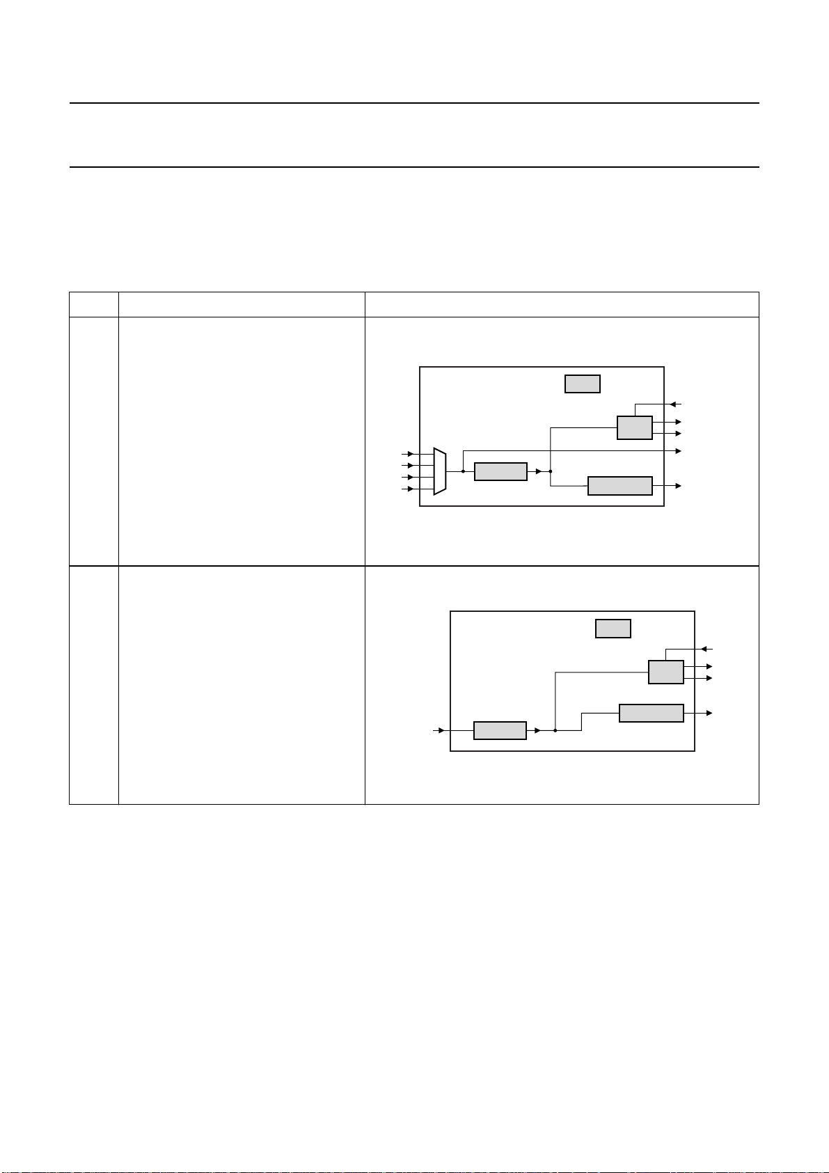
0 Data path:
2
• Input SPDIF to outputs DAC, I
SPDIFOUT via loop through.
Features:
• System locks onto the SPDIF input
signal
• BCK and WS are master
• Microcontroller mode:
– DAC sound features can be used
– SPDIF input channel status bits
(two times 40 bits) can be read.
S or
SPDIF IN
SPDIF LOCK
PLL
MUTE
DAC
SPDIFOUT
I2S OUTPUT I2S master
MGU836
1 Data path:
• Input I
(level II not guaranteed: depends on
I2S-bus clock).
Features:
• System locks onto the WSI signal
• BCKI and WSI are slave
• Microcontroller mode:
– DAC sound features can be used
– SPDIF output channel status bits
(two times 40 bits) setting.
2
S to outputs DAC or SPDIF
I2S slave
I2S INPUT
PLL
I2S LOCK
MUTE
DAC
SPDIF OUT
MGU837
2003 Apr 10 21
Page 22
Philips Semiconductors Preliminary specification
Stereo audio codec with SPDIF interface UDA1355H
MODE FEATURES SCHEMATIC
2 Data path:
• Input SPDIF to outputs I
SPDIFOUT via loop through
• Input I2S to output DAC.
Features:
• Possibility to process input SPDIF via
2
S-bus using an external DSP and
I
then to output DAC
• System locks onto the SPDIF input
signal
• I2S input and output with BCK and WS
are master
• Microcontroller mode: see Section 8.4.
2
S or
SPDIF IN
I2S INPUT
I2S slave
EXTERNAL DSP
(e.g. equalizing, spatializing)
(SAA7715)
PLL
I2S OUTPUT
SPDIF LOCK
DAC
2
S master
I
MGU838
MUTE
SPDIFOUT
3 Data path:
• Input ADC to outputs I
Features:
• Crystal oscillator generates the clocks
• Microcontroller mode:
– PGA gain setting
– Volume control in decimator setting
– SPDIF output channel status bits
(two times 40 bits) setting.
4 Data path:
• Input ADC to output I
• Input I2S to outputs DAC or SPDIF.
Features:
• Possibility to process input ADC via
2
S-bus using a external DSP and then
I
to outputs DAC or SPDIF
• Crystal oscillator generates the clocks
• I2S input and output with BCK and WS
are master
• Microcontroller mode: see Section 8.4.
2
S or SPDIF.
2
S
ADC
ADC
I
2
XTAL
XTAL
S INPUT
I2S slave
EXTERNAL DSP
(e.g. equalizing, spatializing)
(SAA7715)
SPDIF OUT
I2S OUTPUT
MGU839
DAC
SPDIF OUT
2
I
S OUTPUT
I2S master
MGU840
I2S master
MUTE
2003 Apr 10 22
Page 23
Philips Semiconductors Preliminary specification
Stereo audio codec with SPDIF interface UDA1355H
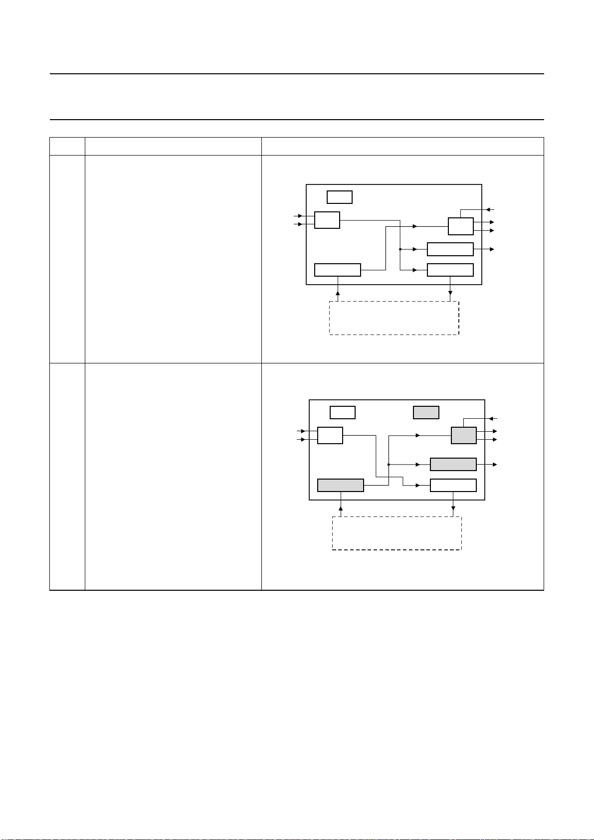
MODE FEATURES SCHEMATIC
5 Data path:
• Input ADC to outputs I
• Input I2S to output DAC.
Features:
• Possibility to process input ADC via
2
I
S-bus using an external DSP and
then to output DAC
• Crystal oscillator generates the clocks
• I2S input and output with BCK and WS
are master
• Microcontroller mode: see Section 8.4.
2
S or SPDIF
XTAL
ADC
2
I
S INPUT
I2S slave
EXTERNAL DSP
(e.g. equalizing, spatializing)
(SAA7715)
DAC
SPDIF OUT
2
I
S OUTPUT
I2S master
MGU841
MUTE
6 Data path:
• Input ADC to output I
• Input I2S to outputs DAC or SPDIF
(level II not guaranteed: depends on
I2S-bus clock).
Features:
• Possibility to process input ADC via
2
I
S-bus using an external DSP and
then to outputs DAC or SPDIF
• Crystal oscillator generates the clocks
for input ADC and output I2S
• WSI is slave
• WSO is master
• Microcontroller mode: see Section 8.4.
2
S
I2S LOCK
XTAL
I2S INPUT
I2S slave
EXTERNAL DSP
(SAA7715)
PLL
SPDIF OUT
I
DACADC
2
S OUTPUT
I2S master
MGU842
MUTE
2003 Apr 10 23
Page 24

Philips Semiconductors Preliminary specification
Stereo audio codec with SPDIF interface UDA1355H
MODE FEATURES SCHEMATIC
7 Data path:
• Input SPDIF to output DAC
• Input ADC to outputs SPDIF or I
Features:
• Crystal oscillator generates the clocks
for outputs SPDIF and I
2
S
• PLL locks onto the SPDIF input signal
• WS of I2S output is master
• Microcontroller mode:
– Decimator features can be used
– DAC sound features can be used
– SPDIF input channel status bits
(two times 40 bits) can be read
– SPDIF output channel status bits
(two times 40 bits) setting.
2
S.
SPDIF LOCK
XTAL
ADC
SPDIF IN
PLL
I
DAC
SPDIF OUT
2
S OUTPUT
MGU843
MUTE
I2S master
8 Data path:
• Input ADC to outputs SPDIF or I
• Input I2S to output DAC.
Features:
• Possibility to process input ADC, via
2
I
S-bus using an external DSP and
then to output DAC
• Crystal oscillator generates the clocks
for outputs SPDIF and I2S
• WSI is slave
• WSO master
• Microcontroller mode:
– Decimator features can be used
– DAC sound features can be used
– SPDIF output channel status bits
(two times 40 bits) setting.
2
S
I2S LOCK
XTAL
ADC
I2S INPUT
I2S slave
EXTERNAL DSP
(e.g. Sample Rate Convertor)
(SAA7715)
PLL
SPDIF OUT
2
I
MUTE
DAC
S OUTPUT
I2S master
MGU844
2003 Apr 10 24
Page 25

Philips Semiconductors Preliminary specification
Stereo audio codec with SPDIF interface UDA1355H
MODE FEATURES SCHEMATIC
9 Data path:
• Input SPDIF to output I
• Input I2S to outputs DAC or SPDIF.
Features:
• Possibility to process input SPDIF, via
2
I
S-bus using an external DSP and
then to outputs DAC or SPDIF
• BCKand WS being master for both I2S
input and output (different clocks)
• Input I2S to outputs DAC and SPDIF;
BCK and WS being master; clocks
based on crystal oscillator
• Microcontroller mode:
– DAC sound features can be used
– SPDIF output channel status bits
(two times 40) setting.
2
S
SPDIF LOCK
XTAL
SPDIF IN
2
I
S INPUT
I2S slave
EXTERNAL DSP
(e.g. Sample Rate Convertor)
(SAA7715)
PLL
SPDIF OUT
I2S OUTPUT
MGU845
DAC
2
S master
I
MUTE
10 Data path:
• Input SPDIF to output DAC or I
• Input I2S-bus to output SPDIF.
Features:
• Possibility to process input SPDIF, via
2
I
S-bus using an external DSP and
then to output SPDIF
• Input SPDIF to outputs I2S and DAC;
locking onto the SPDIF input signal;
BCK and WS being master
• Input I2S to output SPDIF; BCK and
WS being master; clocks are
generated by the crystal oscillator
• Microcontroller mode:
– DAC sound features can be used
– SPDIF input channel status bits
(two times 40) can be read
– SPDIF output channel status bits
(two times 40) setting.
11 Not used
12 See microcontroller mode
13 See microcontroller mode
14 See microcontroller mode
15 Not used
2
S
SPDIF LOCK
XTAL
SPDIF IN
2
I
S INPUT
I2S slave
EXTERNAL DSP
(e.g. Sample Rate Convertor)
(SAA7715)
PLL
SPDIF OUT
I2S OUTPUT
MGU846
DAC
2
S master
I
MUTE
2003 Apr 10 25
Page 26

Philips Semiconductors Preliminary specification
Stereo audio codec with SPDIF interface UDA1355H
8.3 Microcontroller mode pin assignment
In microcontroller mode all features become available, such as volume control, PGA gain and mixing (in some modes).
The pin functions are defined in Table 12.
Table 12 Microcontroller mode pin assignment
PIN
SYMBOL
L3-BUS
SYMBOL
I2C-BUS
LEVEL DESCRIPTION
4 LOCK LOCK LOW FPLL and SPDIF are out of LOCK
HIGH FPLL in lock when SPDIF is not used; FPLL or SPDIF in lock when
SPDIF is used
16 RESET RESET LOW normal operation
HIGH reset
17 no function no function LOW connect to ground
18 A0 A0 − A0 address input/output bit (for microcontroller register)
19 U_RDY U_RDY LOW user bit stable
HIGH new user bit
20 SEL_STATIC SEL_STATIC MID I
2
C-bus mode
LOW L3-bus mode
HIGH static mode
21 USER USER − user bit output (new bit every SPDIF sub-frame)
22 AC3 AC3 LOW no I
HIGH I
29 L3MODE no function − L3MODE for L3-bus mode; no function for I
30 L3CLOCK SCL − L3CLOCK for L3-bus mode or SCL for I
31 L3DATA SDA − L3DATA for L3-bus mode or SDA for I
2
S-bus data preamble detected
2
S-bus data preamble detected
2
C-bus
2
C-bus mode
2
C-bus mode
44 MUTE MUTE LOW no mute
HIGH mute active
2003 Apr 10 26
Page 27

Philips Semiconductors Preliminary specification
Stereo audio codec with SPDIF interface UDA1355H
8.4 Microcontroller mode applications
In Table 13, the encoding of bits MODE[3:0] in the microcontroller mode is given.
Table 13 Microcontroller mode applications
MODE BITS CLOCK
MODE
MODE[3:0]
SPDIF
INPUT
SPDIF
OUTPUT
ADC DAC
0 0000 PLL PLL − PLL - PLL SPDIF
1 0001 − PLL − PLL PLL − I2S
2 0010 PLL PLL PLL PLL PLL PLL SPDIF
3 0011 − xtal xtal −−xtal −
4 0100 − xtal xtal xtal xtal xtal −
5 0101 − xtal xtal xtal xtal xtal −
6 0110 − PLL xtal PLL PLL xtal I
7 0111 PLL xtal xtal PLL − xtal SPDIF
8 1000 − xtal xtal PLL PLL xtal I
9 1001 PLL xtal xtal xtal xtal PLL SPDIF
10 1010 PLL xtal PLL PLL xtal PLL SPDIF
11 1011 not used
12 1100 PLL xtal xtal PLL PLL xtal SPDIF
13 1101 PLL PLL xtal PLL PLL xtal SPDIF
14 1110 − PLL PLL PLL PLL PLL I
15 1111 not used
(1)
I2S-BUS
INPUT
SLAVE
I2S-BUS
OUTPUT
MASTER
PLL
LOCKS
ON
INPUT
2
S
2
S
2
S
Note
1. In column clock means:
xtal: the clock is based on the crystal oscillator; PLL: the clock is based on the PLL.
2003 Apr 10 27
Page 28

Philips Semiconductors Preliminary specification
Stereo audio codec with SPDIF interface UDA1355H
In the microcontroller mode, more features are available. The application modes are given in Table 14. Some modes are
the same in terms of data path as for the static mode. These modes are already explained in Section 8.2. Some modes
are combined into one mode (like modes 4 and 5).
Table 14 Overview of microcontroller modes
MODE FEATURE SCHEMATIC
0 See static mode
1 See static mode
2 Data path:
2
• Inputs ADC, I
DAC, I2S or SPDIF.
Features:
• All clocks are related to the SPDIF
clock
2
S input and output have master BCK
• I
and WS
• SPDIF input channel status bits (two
times 40) can be read
• OutputSPDIFsupported but the timing
not according to level II: depends on
I2S-bus clock
• Output SPDIFOUT loop through can
be selected with independent SPDIF
input channel select.
S and SPDIF to outputs
ADC
SPDIF IN
I2S INPUT
PLL
I2S slave
EXTERNAL DSP
(e.g. equalizing, spatializing)
(SAA7715)
SPDIF LOCK
DAC
SPDIF
OUT
I2S OUTPUT
2
I
MGU847
MUTE
SPDIF OUT
S master
3 See static mode
4 + 5 Data path:
• Inputs ADC and I2S to outputs DAC,
I2S or SPDIF.
Features:
• Mode 4 and 5 are combined in
microcontroller mode
• Crystal oscillator generates the clocks
2
S input and output have master BCK
• I
and WS
• SPDIF output channel status bits (two
times 40) setting.
2003 Apr 10 28
ADC
2
I
S INPUT
XTAL
I2S slave
EXTERNAL DSP
(e.g. equalizing, spatializing)
(SAA7715)
DAC
SPDIF OUT
2
I
S OUTPUT
I2S master
MGU848
MUTE
Page 29

Philips Semiconductors Preliminary specification
Stereo audio codec with SPDIF interface UDA1355H
MODE FEATURE SCHEMATIC
6 See static mode
7 See static mode
8 See static mode
9 Data path:
• Inputs ADC and I
SPDIF
• Input SPDIF to output I2S.
Features:
• Input SPDIF to output I
and WS being master; the clocks for
this are recovered from the SPDIF
input signal
• Therestoftheclocksaregeneratedby
the crystal oscillator
• SPDIF input channel status bits (two
times 40) can be read
• SPDIF output channel status bits (two
times 40) setting
• Possibility to process input SPDIF, via
I2S-bus using an external DSP and
then to outputs DAC or SPDIF.
2
S to outputs DAC or
2
S with BCK
XTAL
ADC
SPDIF IN
2
I
S INPUT
I2S slave
EXTERNAL DSP
(e.g. Sample Rate Convertor)
(SAA7715)
PLL
SPDIF OUT
I2S OUTPUT
SPDIF LOCK
DAC
2
S master
I
MGU849
MUTE
10 Data path:
• InputsADC and SPDIF to outputs DAC
or I2S
• Input I2S to output SPDIF.
Features:
• BCK and WS are master
• SPDIF input channel status bits (two
times 40) can be read
• SPDIF output channel status bits (two
times 40) setting
• Possibility to process inputs ADC or
SPDIF, via I
2
S-bus using an external
DSP and then to output SPDIF.
11 Not used
XTAL
ADC
SPDIF IN
2
I
S INPUT
I2S slave
EXTERNAL DSP
(e.g. Sample Rate Convertor)
(SAA7715)
PLL
SPDIF OUT
I2S OUTPUT
SPDIF LOCK
DAC
2
I
S master
MGU850
MUTE
2003 Apr 10 29
Page 30

Philips Semiconductors Preliminary specification
Stereo audio codec with SPDIF interface UDA1355H
MODE FEATURE SCHEMATIC
12 Data path:
• Input ADC to outputs I
• Inputs I2S and SPDIF to output DAC.
Features:
• BCK and WS of I
• Inputs SPDIF and I2S to output DAC
withmixing/selection possibility; clocks
aregenerated fromSPDIFinput signal,
and BCK and WS are master
• SPDIF input channel status bits (two
times 40) can be read
• SPDIF output channel status bits (two
times 40) setting.
2
S or SPDIF
2
S output are master
XTAL
ADC
SPDIF IN
I2S INPUT
PLL
I
SPDIF LOCK
DAC
SPDIF OUT
2
S OUTPUT
MGU851
MUTE
I2S masterI2S slave
13 Data path:
• Input ADC to output I
2
S
• Inputs I2S and SPDIF to outputs DAC
or SPDIF.
Features
• BCK and WS being master
• SPDIF input channel status bits (two
times 40) can be read
• OutputSPDIFsupported but the timing
not according to level II
• Output SPDIFOUT loop through can
be selected with independent SPDIF
input channel select.
14 Data path:
2
• Inputs ADC and I
S to outputs DAC
SPDIF and I2S.
Features:
• All clocks are related to WS signal of
2
I
S-bus input
• Master BCK and WS for I2S output;
slave BCK and WS for I2S input
• SPDIF output channel status bits (two
times 40) can be set; level II timing
depends on the I2S-bus clocks.
2
S slave
I
XTAL
ADC
SPDIF IN
I2S INPUT
ADC
I2S INPUT
PLL
SPDIF
OUT
2
I
S OUTPUT
PLL
SPDIF OUT
I2S OUTPUT
SPDIF LOCK
MUTE
DAC
SPDIF OUT
I2S master
MGU852
I2S LOCK
MUTE
DAC
I2S masterI2S slave
15 Not used
2003 Apr 10 30
MGU853
Page 31

Philips Semiconductors Preliminary specification
Stereo audio codec with SPDIF interface UDA1355H
9 SPDIF SIGNAL FORMAT
9.1 SPDIF channel encoding
The digital signal is coded using Biphase Mark Code
(BMC), which is a kind of phase modulation. In this
scheme, a logic 1 in the data corresponds to two
zero-crossings in the coded signal, and a logic 0 to one
zero-crossing. An example of the encoding is given in
Fig.11.
handbook, halfpage
clock
data
BMC
MGU606
Fig.11 Biphase mark encoding.
9.2 SPDIF hierarchical layers
The SPDIF signal format is shown in Fig.12. A PCM signal
is transmitted in sequential blocks. Each block consists
of 192 frames. Each frame contains two sub-frames, one
for each channel. Each subframe is preceded by a
preamble. There are three types of preambles: B, M
and W. Preambles can be spotted easily in an SPDIF
bitstream because these sequences never occur in the
channel parts of a valid SPDIF bitstream.
The sub-frame format is represented by Fig.13.
A sub-frame contains a single audio sample word which
may be 24 bits wide, a validity bit which indicates whether
the sample is valid, a bit containing user data, a bit
indicating the channel status and a parity bit for this
sub-frame.
Thedata bits 31 to 4 in each sub-frame are encodedusing
a BMC scheme. The sync preamble contains a violation of
the BMC scheme and can be detected. Table 15 indicates
the values of the preambles.
handbook, full pagewidth
channel 1MMMWW WBchannel 2 channel 1
handbook, full pagewidth
03478 27 28 31
sync
preamble
L
S
B
auxiliary
sub-frame
L
S
B
channel 2 channel 1 channel 2 channel 1 channel 2
sub-frame
frame 0 frame 191frame 191
block
Fig.12 SPDIF signal format
validity flag
user data
channel status
parity bit
MGU607
M
S
B
CUV
MGU608
Paudio sample word
Fig.13 Sub-frame format
2003 Apr 10 31
Page 32

Philips Semiconductors Preliminary specification
Stereo audio codec with SPDIF interface UDA1355H
Table 15 Preambles
PRECEDING
STATE
CHANNEL CODING
01
B 11101000 00010111
M 11100010 00011101
W 11100100 00011011
9.3 Timing characteristics
9.3.1 F
REQUENCY REQUIREMENTS
The SPDIF specification IEC 60958 supports three levels
of clock accuracy:
• Level I high accuracy: Tolerance of transmitting
sampling frequency shall be within 50 × 10
−6
• Level II, normal accuracy: All receivers should receive a
signal of 1000 × 10−6 of nominal sampling frequency
• Level III, variable pitch shifted clock mode: A deviation
of 12.5% of the nominal sampling frequency is possible.
The UDA1355H inputs support level I, II, and III as
specified by the IEC 60958 standard.
9.3.2 RISE AND FALL TIMES
Rise and fall times (see Fig.14) are defined as:
t
Rise time =
Fall time =
--------------tLtH+
t
f
--------------tLtH+
r
100%×
100%×
Rise and fall times should be in the range:
• 0% to 20% when the data bit is a logic 1
• 0% to 10% when the data bits are two succeeding
logic 0.
9.3.3 D
UTY CYCLE
The duty cycle (see Fig.14) is defined as:
t
Duty cycle =
H
--------------tLtH+
100%×
The duty cycle should be in the range:
• 40% to 60% when the data bit is a logic 1
• 45% to 55% when the data bits are two succeeding
logic 0.
10 L3-BUS DESCRIPTION
Theexchange of data and control information between the
microcontroller and the UDA1355H is accomplished
through a serial hardware L3-bus interface comprising the
following pins:
• MP0: mode line with signal L3MODE
• MP1: clock line with signal L3CLOCK
• MP2: data line with signal L3DATA.
The exchange of bytes in L3-bus mode is LSB first.
The L3-bus format has two modes of operation:
• Address mode
• Data transfer mode.
The address mode is used to select a device for a
subsequent data transfer. The address mode is
characterized by L3MODE being LOW and a burst of
8 pulses on L3CLOCK, accompanied by 8 bits (see
Fig.15). The data transfer mode is characterized by
L3MODE being HIGH and is used to transfer one or more
bytes representing a register address, instruction or data.
Basically two types of data transfers can be defined:
• Write action: data transfer to the device
• Read action: data transfer from the device.
handbook, halfpage
90%
50%
10%
t
H
t
r
t
L
t
f
MGU612
Fig.14 Rise, fall time and duty cycle.
2003 Apr 10 32
10.1 Device addressing
The device address consists of one byte with:
• Data Operating Mode (DOM) bits 0 and 1 representing
the type of data transfer (see Table 16)
• Address bits 2 to 7 representing a 6-bit device address.
Page 33

Philips Semiconductors Preliminary specification
Stereo audio codec with SPDIF interface UDA1355H
Table 16 Selection of data transfer
DOM BITS
BIT 0 BIT 1
0 0 not used
1 0 not used
0 1 write data or prepare read
1 1 read data
ThedeviceaddressoftheUDA1355Hisgiven in Table 17,
being the first 6 bits of the device address byte. The
address can be set one of two by using pin MODE1
(pin A0 in microcontroller mode).
Table 17 L3-bus device address
MSB ADDRESS LSB
00001A0
Remark: When using the device address, there is often
misunderstanding. This is caused by the fact that the data
is sent LSB first. This means that when we use the device
address in, for example the Philips L3-bus/I
bithacker’, we have to use the address like LSB → MSB.
For the UDA1355H this means that the device address to
be used is either 10H (010000) or 30H (110000).
10.2 Register addressing
After sending the device address, including Data
Operating Mode (DOM) bits indicating whether the
information is to be read or written, one data byte is sent
using bit 0 to indicate whether the information will be read
or written and bits 1 to 7 for the destination register
address.
Basically there are three methods for register addressing:
• Addressing for write data: bit 0 is logic 0 indicating a
write action to the destination register, followed by
bits 1 to 7 indicating the register address (see Fig.15)
• Addressing for prepare read: bit 0 is logic 1 indicating
that data will be read from the register (see Fig.16)
• Addressing for data read action: in this case the device
returnsaregisteraddresspriortosendingdata from that
register. When bit 0 is logic 0, the register address is
valid; in case bit 0 is logic 1 the register address is
invalid.
TRANSFER
2
C-bus
10.3 Data write mode
The data write mode is explained in the signal diagram of
Fig.15.
For writing data to a device, 4 bytes must be sent (see
Table 18):
• Byte 1 starting with 01 for signalling the write action to
the device, followed by the device address
• Byte 2 starting with 0 for signalling the write action,
followed by 7 bits indicating the destination address in
binary format with A6 being the MSB and A0 being the
LSB
• Byte 3 with bit D15 being the MSB
• Byte 4 with bit D0 being the LSB.
Itshould be noted that each time anewdestinationregister
address needs to be written, the device address must be
sent again.
10.4 Data read mode
For reading data from the device, first a prepare read must
be done and then data read. The data read mode is
explained in the signal diagram of Fig.16.
For reading data from a device, the following 6 bytes are
involved (see Table 19):
• Byte 1 with the device address including 01 for
signalling the write action to the device
• Byte 2 is sent with the register address from which data
needstobe read. This byte starts with 1, which indicates
thattherewillbe a read action from the register, followed
again by 7 bits for the destination address in binary
format with A6 being the MSB and A0 being the LSB
• Byte 3with the device address including 11issentto the
device. The 11 indicates that the device must write data
to the microcontroller
• Byte 4, sent by the device to the bus, with the
(requested) register address and a flag bit indicating
whether the requested register was valid (bit is logic 0)
or invalid (bit is logic 1)
• Byte 5, sent by the device to the bus, with the data
information in binary format with D15 being the MSB
• Byte 6, sent by the device to the bus, with the data
information in binary format with D0 being the LSB.
2003 Apr 10 33
Page 34

Philips Semiconductors Preliminary specification
Philips Semiconductors Preliminary specification
Stereo audio codec with SPDIF interface UDA1355H
Stereo audio codec with SPDIF interface UDA1355H
MGS754
MGS753
data byte 1 data byte 2
data byte 1 data byte 2
register address
write
device address
10
0
DOM bits
Fig.15 Data write mode.
0/1
register address device address register address
1
valid/non-valid
Fig.16 Data read mode.
read
prepare read send by the device
This text is here in white to force landscape pages to be rotated correctly when browsing through the pdf in the Acrobat reader.This text is here in
_white to force landscape pages to be rotated correctly when browsing through the pdf in the Acrobat reader.This text is here inThis text is here in
white to force landscape pages to be rotated correctly when browsing through the pdf in the Acrobat reader. white to force landscape pages to be ...
2003 Apr 10 34
2003 Apr 10 34
L3 wake-up pulse after power-up
L3CLOCK
L3MODE
L3DATA
L3CLOCK
device address
L3MODE
111
0
DOM bits
L3DATA
Page 35

Philips Semiconductors Preliminary specification
Stereo audio codec with SPDIF interface UDA1355H
Table 18 L3-bus write data
BYTE L3-BUS MODE ACTION
FIRST IN TIME LAST IN TIME
BIT 0 BIT 1 BIT 2 BIT 3 BIT 4 BIT 5 BIT 6 BIT 7
1 address device address 0 1 A0 10000
2 data transfer register address 0 A6 A5 A4 A3 A2 A1 A0
3 data transfer data byte 1 D15 D14 D13 D12 D11 D10 D9 D8
4 data transfer data byte 2 D7 D6 D5 D4 D3 D2 D1 D0
Table 19 L3-bus read data
FIRST IN TIME LAST IN TIME
BYTE L3-BUS MODE ACTION
BIT 0 BIT 1 BIT 2 BIT 3 BIT 4 BIT 5 BIT 6 BIT 7
1 address device address 0 1 A0 10000
2 data transfer register address 1 A6 A5 A4 A3 A2 A1 A0
3 address device address 1 1 A0 10000
4 data transfer register address 0 or 1 A6 A5 A4 A3 A2 A1 A0
5 data transfer data byte 1 D15 D14 D13 D12 D11 D10 D9 D8
6 data transfer data byte 2 D7 D6 D5 D4 D3 D2 D1 D0
11 I2C-BUS DESCRIPTION
11.1 Characteristics
The bus is for 2-way, 2-line communication between
different ICs or modules. The two lines are a Serial Data
Line (SDA) and a Serial Clock Line (SCL). Both lines must
be connected to the supply voltage (VDD) via a pull-up
resistor when connected to the output stages of a
microcontroller. For a 400 kHz IC the recommendation for
this type of bus from Philips Semiconductors must be
11.2 Bit transfer
One data bit is transferred during each clock pulse (see
Fig.17). The data on the SDA line must remain stable
during the HIGH period of the clock pulse as changes in
the data line at this time will be interpreted as control
signals. The maximum clock frequency is 400 kHz. To be
abletorunonthis high frequency all the inputs and outputs
connectedtothisbusmustbedesignedforthishighspeed
2
I
C-bus according the Philips specification.
followed (e.g. up to loads of 200 pF on the bus a pull-up
resistor can be used, between 200 to 400 pF a current
source or switched resistor must be used). Data transfer
can only be initiated when the bus is not busy.
handbook, full pagewidth
SDA
SCL
data line
stable;
data valid
Fig.17 Bit transfer on the I2C-bus.
2003 Apr 10 35
change
of data
allowed
MBC621
Page 36

Philips Semiconductors Preliminary specification
Stereo audio codec with SPDIF interface UDA1355H
11.3 Byte transfer
Each byte (8 bits) is transferred with the MSB first (see
Table 20).
Table 20 Byte transfer
MSB BIT LSB
76543210
11.4 Data transfer
A device generating a message is a transmitter; a device
receiving a message is the receiver. The device that
controls the message is the master and the devices which
are controlled by the master are the slaves.
11.5 Register address
2
The register addresses in the I
C-bus mode are the same
as in the L3-bus mode.
11.6 Device address
Before any data is transmitted on the I2C-bus, the device
whichshouldrespondis addressed first. The addressing is
always done with the first byte transmitted after the start
procedure. The device address can be one of two, being
set by bit A0 which corresponds to pin MODE1.
The UDA1355H acts as a slave receiver or a slave
transmitter. Therefore, the clock signal SCL is only an
input signal. The data signal SDA is a bidirectional line.
The UDA1355H slave address is shown in Table 21.
11.7 Start and stop conditions
Both data and clock line will remain HIGH when the bus in
not busy. A HIGH-to-LOW transition of the data line, while
the clock is HIGH, is defined as a start condition (S).
A LOW-to-HIGH transition of the data line while the clock
is HIGH is defined as a stop condition (P); (see Fig.18).
11.8 Acknowledgment
The number of data bits transferred between the start and
stop conditions from the transmitter to receiver is not
limited. Each byte of eight bits is followed by one
acknowledge bit (see Fig.19). At the acknowledge bit the
data line is released by the master and the master
generates an extra acknowledge related clock pulse.
A slave receiver which is addressed must generate an
acknowledge after the reception of each byte. Also a
master must generate an acknowledge after the reception
of each byte that has been clocked out of the slave
transmitter.
The device that acknowledges has to pull-down the SDA
line during the acknowledge clock pulse, so that the SDA
line is stable LOW during the HIGH period of the
acknowledge related clock pulse. Set-up and hold times
must be taken into account. A master receiver must signal
an end of data to the transmitter by not generating an
acknowledge on the last byte that has been clocked out of
the slave. In this event the transmitter must leave the data
line HIGH to enable the master to generate a stop
condition.
2
Table 21 I
C-bus slave address
DEVICE ADDRESS R/
W
A6 A5 A4 A3 A2 A1 A0 −
0 0 1 1 0 1 A0 0/1
handbook, full pagewidth
SDA
SCL
S
START condition
Fig.18 START and STOP conditions on the I2C-bus.
2003 Apr 10 36
P
STOP condition
SDA
SCL
MBC622
Page 37

Philips Semiconductors Preliminary specification
Stereo audio codec with SPDIF interface UDA1355H
handbook, full pagewidth
DATA OUTPUT
BY TRANSMITTER
not acknowledge
DATA OUTPUT
BY RECEIVER
acknowledge
SCL FROM
MASTER
S
START
condition
Fig.19 Acknowledge on the I2C-bus.
11.9 Write cycle
The write cycle is used to write groups of two bytes to the
internal registers for the digital sound feature control and
system setting. It is also possible to read these locations
for chip status information.
The I2C-bus configuration for a write cycle is shown in
Table 22. The write cycle is used to write the data to the
internal registers. The device and register addresses are
one byte each, the setting data is always a couple of two
bytes.
The format of the write cycle is as follows:
1. The microcontroller starts with a start condition (S).
2. The first byte (8 bits) contains the device address
0011010 and a logic 0 (write) for the R/W bit.
3. This is followed by an acknowledge (A) from the
UDA1355H.
9821
clock pulse for
acknowledgement
MBC602
4. After this the microcontroller writes the 8-bit register
address (ADDR) where the writing of the register
content of the UDA1355H must start.
5. The UDA1355H acknowledges this register address
(A).
6. The microcontroller sends two bytes data with the
Most Significant (MS) byte first and then the Least
Significant (LS) byte. After each byte an acknowledge
is followed from the UDA1355H.
7. If repeated groups of two bytes are transmitted, then
the register address is auto incremented. After each
byte an acknowledge is followed from the
microcontroller.
8. Finally, the UDA1355H frees the I2C-bus and the
microcontroller can generate a stop condition (P).
2
Table 22 Master transmitter writes to the UDA1355H registers in the I
DEVICE
ADDRESS
R/W
REGISTER
ADDRESS
DATA 1 DATA 2
C mode.
(1)
DATA n
(1)
S 0011010 0 A ADDR A MS1 A LS1 A .... A ..... A MSn A LSn A P
acknowledge from UDA1355H
Note
1. Auto increment of register address.
2003 Apr 10 37
Page 38

Philips Semiconductors Preliminary specification
Philips Semiconductors Preliminary specification
Stereo audio codec with SPDIF interface UDA1355H
Stereo audio codec with SPDIF interface UDA1355H
(1)
DATA n
(1)
C-bus configuration for a read cycle is shown in Table 23
2
R/W DATA 1 DATA 2
C-bus mode
2
DEVICE
ADDRESS
C-bus and the microcontroller can generate a stop condition (P).
2
ADDRESS
REGISTER
acknowledge from UDA1355H acknowledge from master
R/W
This text is here in white to force landscape pages to be rotated correctly when browsing through the pdf in the Acrobat reader.This text is here in
_white to force landscape pages to be rotated correctly when browsing through the pdf in the Acrobat reader.This text is here inThis text is here in
white to force landscape pages to be rotated correctly when browsing through the pdf in the Acrobat reader. white to force landscape pages to be ...
11.10 Read cycle
The read cycle is used to read the data values from the internal registers. The I
2003 Apr 10 38
2003 Apr 10 38
(A) follows from the UDA1355H.
acknowledged follows from the microcontroller.
microcontroller.
The format of the read cycle is as follows:
1. The microcontroller starts with a start condition (S).
2. The first byte (8 bits) contains the device address 0011010 and a logic 0 (write) for the R/W bit.
3. This is followed by an acknowledge (A) from the UDA1355H.
4. After this microcontroller writes the 8-bit register address (ADDR) where the reading of the register content of the UDA1355H must start.
5. The UDA1355H acknowledges this register address (A).
6. Then the microcontroller generates a repeated start (Sr).
7. Then the microcontroller generates the device address 0011010 again, but this time followed by a logic 1 (read) of the R/W bit. An acknowledge
8. The UDA1355H sends two bytes data with the Most Significant (MS) byte first and then the Least Significant (LS) byte. After each byte an
9. If repeated groups of two bytes are transmitted, then the register address is auto incremented. After each byte an acknowledge follows from the
10. The microcontroller stops this cycle by generating a Negative Acknowledge (NA).
DEVICE
ADDRESS
Table 23 Master transmitter reads from the UDA1355H registers in the I
11. Finally, the UDA1355H frees the I
S 0011010 0 A ADDR A Sr 0011010 1 A MS1 A LS1 A ... A ... A MSn A LSn NA P
Note
1. Auto increment of register address.
Page 39

Philips Semiconductors Preliminary specification
Stereo audio codec with SPDIF interface UDA1355H
12 REGISTER MAPPING
In this chapter the register addressing of the microcontroller interface of the UDA1355H is given. In Section 12.1, the
mapping of the readable and writable registers is given. The explanation of the register definitions are explained in
Sections 12.2 and 12.3.
12.1 Address mapping
Table 24 Register map settings
ADDRESS R/W DESCRIPTION
System settings
00H R/W crystal clock power-on setting; crystal clock and PLL divider settings; MODE and WS detector
settings; clock output setting
01H R/W I2S-bus output format settings
02H R/W I
03H R/W reserved for manufacturers evaluation and should be kept untouched for normal operation
04H R/W analog power and clock settings
Interpolator
10H R/W master volume control settings
11H R/W mixer volume settings
12H R/W sound feature and bass boost and treble settings
13H R/W gain select; de-emphasis and mute settings
14H R/W DACpolarity; noise shaper selection; mixer; source selection; silence detector and interpolator
18H R mute and silence detector status read-out
19H R/W resonant bass boost coefficient k1 setting
1AH R/W resonant bass boost coefficient km setting
1BH R/W resonant bass boost coefficient a1 setting
1CH R/W resonant bass boost coefficient a2 setting
1DH R/W resonant bass boost coefficient b1 setting
1EH R/W resonant bass boost coefficient b2m setting
Decimator
20H R/W ADC gain settings
21H R/W ADC mute and PGA gain settings;
22H R/W ADC polarity and DC cancellation settings
28H R mute status and overflow ADC read-out
SPDIF input
30H R/W SPDIF power control and SPDIF input settings
40H R/W reserved for manufacturers evaluation and should be kept untouched for normal operation
59H R SPDIF LOCK; bit error information and SPDIF encoder output status read-out
5AH R SPDIF input status bits 15 to 0 left channel read-out
5BH R SPDIF input status bits 31 to 16 left channel read-out
5CH R SPDIF input status bits 39 to 32 left channel read-out
2
S-bus input format settings
oversampling settings
2003 Apr 10 39
Page 40

Philips Semiconductors Preliminary specification
Stereo audio codec with SPDIF interface UDA1355H
ADDRESS R/W DESCRIPTION
5DH R SPDIF input status bits 15 to 0 right channel read-out
5EH R SPDIF input status bits 31 to 16 right channel read-out
5FH R SPDIF input status bits 39 to 32 right channel read-out
SPDIF output
50H R/W SPDIF output valid; left to right channel status bit copy; power control and SPDIF output
selection setting
51H R/W SPDIF output status bits 39 to 24 left channel setting
52H R/W SPDIF output status bits 23 to 8 left channel setting
53H R/W SPDIF output status bits 7 to 0 left channel setting
54H R/W SPDIF output status bits 39 to 24 right channel setting
55H R/W SPDIF output status bits 23 to 8 right channel setting
56H R/W SPDIF output status bits 7 to 0 right channel setting
60H R/W reserved for manufacturers evaluation and should be kept untouched for normal operation
61H R/W reserved for manufacturers evaluation and should be kept untouched for normal operation
62H R/W reserved for manufacturers evaluation and should be kept untouched for normal operation
63H R/W reserved for manufacturers evaluation and should be kept untouched for normal operation
64H R/W reserved for manufacturers evaluation and should be kept untouched for normal operation
Device ID
7EH R device ID; version
Software reset
7FH R/W restore L3-bus defaults
12.2 Read/write registers mapping
12.2.1 SYSTEM SETTINGS
Table 25 Register address 00H
BIT 15 14 13 12 11 10 9 8
Symbol EXPU − PON_XTAL
PLL
Default 0 0 1 0 1 0 0 0
BIT 7 6 5 4 3 2 1 0
Symbol MODE3 MODE2 MODE1 MODE0 ws_detct_EN ws_detct_set CLKOUT_
Default 0 0 1 0 1 0 1 0
XTL_DIV4 XTL_DIV3 XTL_DIV2 XTL_DIV1 XTL_DIV0
CLKOUT_
SEL1
SEL0
2003 Apr 10 40
Page 41

Philips Semiconductors Preliminary specification
Stereo audio codec with SPDIF interface UDA1355H
Table 26 Description of register bits (address 00H)
BIT SYMBOL DESCRIPTION
15 EXPU EXPU. Bit EXPU is reserved for manufacturers evaluation and should be kept
untouched for normal operation of UDA1355H.
14 − reserved
13 PON_XTALPLL Power control crystal oscillator and PLL. If this bit is logic 0, then the crystal
oscillator and PLL are turnedoff; if this bit is logic 1, then the crystal oscillator and PLL
are running.
12 to 8 XTL_DIV[4:0] Crystal oscillator clock divider setting. Value to select the sampling frequency and
the system clock output frequency (256f
BCKI and BCKO clock frequency of digital interface running with crystal oscillator clock
will be 64fs; when 384fs is selected, it will be 48fs (see Table 27).
7 to 4 MODE[3:0] Microcontroller application mode setting. Value to select the microcontroller
application mode (see Table 28).
3 ws_detct_EN Word select detector enable.If this bit is logic 0, then WS detector is disabled; if this
bit is logic 1, then WS detector is enabled.
2 ws_detct_set Word select detector limit setting. If this bit is logic 0, then the lower frequency limit
of the WS detector is 4095 clock cycles (3 kHz); if this bit is logic 1, then the lower
frequency limit of the WS detector is 2047 clock cycles (6 kHz).
1 and 0 CLKOUT_SEL[1:0] Clock output select. If these bits are 00 or 10, then the BCKI and BCKO clock
frequency of digital interface running with FPLL clock will be 64f
48fs. The selection between 256fsand 384fs for the crystal clock output is set via the
bits XTL_DIV[4:0]:
00 = FPLL clock 256f
01 = FPLL clock 384f
s
s
10 = crystal clock
11 = crystal clock
or 384fs). When 256fsis selected, the master
s
; otherwise, it will be
s
Table 27 Crystal oscillator output frequencies
XTL_DIV4 XTL_DIV3 XTL_DIV2 XTL_DIV1 XTL_DIV0 OUTPUT RATE
Based on 32 kHz
00000256×16 kHz
00001384×16 kHz
00010256×32 kHz
00011384×32 kHz
00100256×64 kHz
00101384×64 kHz
Based on 44.1 kHz
00110256×22.05 kHz
00111384×22.05 kHz
01000256×44.1 kHz
01001384×44.1 kHz
01010256×88.2 kHz
01011384×88.2 kHz
2003 Apr 10 41
Page 42

Philips Semiconductors Preliminary specification
Stereo audio codec with SPDIF interface UDA1355H
XTL_DIV4 XTL_DIV3 XTL_DIV2 XTL_DIV1 XTL_DIV0 OUTPUT RATE
Based on 48 kHz
01100256×24 kHz
01101384×24 kHz
01110256×48 kHz
01111384×48 kHz
10000256×96 kHz
10001384×96 kHz
Table 28 Application mode selection
MODE3 MODE2 MODE1 MODE0 FUNCTION
0000mode 0
0001mode 1
0010mode 2
0011mode 3
0100mode 4
0101mode 5
0110mode 6
0111mode 7
1000mode 8
1001mode 9
1010mode 10
1011mode 11
1100mode 12
1101mode 13
1110mode 14
1111mode 15
Table 29 Register address 01H
BIT 15 14 13 12 11 10 9 8
Symbol −−− −− − −MUTE_DAO
Default 0 0 0 0 0 0 0 0
BIT 7 6 5 4 3 2 1 0
Symbol PON_DIGO − DIGOUT1 DIGOUT0 − SFORO2 SFORO1 SFORO0
Default 1 0 1 0 0 0 0 0
2003 Apr 10 42
Page 43

Philips Semiconductors Preliminary specification
Stereo audio codec with SPDIF interface UDA1355H
Table 30 Description of register bits (address 01H)
BIT SYMBOL DESCRIPTION
15 to 9 − reserved
8 MUTE_DAO Digital mute setting. If this bit is logic 0, then the digital output is not muted; if this bit is
logic 1, then the digital output is muted.
7 PON_DIGO Power control digital output. If this bit is logic 0, then the digital output is in Power-down
mode; if this bit is logic 1, then the digital output is in power-on mode. The registers have
their own clock, which means that there cannot be a dead-lock situation.
6 − reserved
5 and 4 DIGOUT[1:0] Input selector for digital output. Value to select the input signal for the digital output. The
default input will be chosen if in an application an invalid data signal is selected:
00 = ADC input
01 = digital input
10 = IEC 60958 input
11 = interpolator mixer output
3 − reserved
2 to 0 SFORO[2:0] Digital output format. Value to set the digital output format:
2
000 = I
001 = LSB-justified; 16 bits
010 = LSB-justified; 18 bits
011 = LSB-justified; 20 bits
100 = LSB-justified; 24 bits
101 = MSB-justified
110 = not used; output is default value
111 = not used; output is default value
S-bus
Table 31 Register address 02H
BIT 15 14 13 12 11 10 9 8
Symbol − −−−− − − −
Default 0 00000 0 0
BIT7 6543 2 1 0
Symbol PON_DIGI −−−−SFORI2 SFORI1 SFORI0
Default 1 00000 0 0
Table 32 Description of register bits (address 02H)
BIT SYMBOL DESCRIPTION
15 to 8 − reserved
7 PON_DIGI Power control digital input. If this bit is logic 0, then the digital input is in Power-down
mode; if this bit is logic 1, then the digital input is in power-on mode. The registers have their
own clock, which means that there cannot be a dead-lock situation.
6to3 − reserved
2003 Apr 10 43
Page 44

Philips Semiconductors Preliminary specification
Stereo audio codec with SPDIF interface UDA1355H
BIT SYMBOL DESCRIPTION
2 to 0 SFORI[2:0] Digital input format. Value to set the digital input format:
2
000 = I
001 = LSB-justified; 16 bits
010 = LSB-justified; 18 bits
011 = LSB-justified; 20 bits
100 = LSB-justified; 24 bits
101 = MSB-justified
110 = not used; input is default value
111 = not used; input is default value
Table 33 Register address 04H
BIT 15 14 13 12 11 10 9 8
Symbol PON_DAC − −−−PON_ADCL PON_ADCR PON_ADC_bias
Default 1 0 0 0 0 1 1 1
S-bus
BIT
Symbol DACLK_OFF DACLK_AUTO −−−EN_DEC − EN_INT
Default 0 0 0 0 0 1 0 1
Table 34 Description of register bits (address 04H)
BIT SYMBOL DESCRIPTION
15 PON_DAC Power control DAC. If this bit is logic 0, then the DAC is in Power-down mode; if this bit
14 to 11 − reserved
10 PON_ADCL Power control ADC left channel. Value to set power on the ADC left channel (see
9 PON_ADCR Power control ADC right channel. Value to set power on the ADC right channel (see
8 PON_ADC_bias Power control ADC bias. Value to set power on the ADCs (see Table 35).
7 DACLK_OFF DAC clock enable. If this bit is logic 0, then the DAC clock is disabled; if this bit is
6 DACLK_AUTO DAC clock auto function. If this bit is logic 0, then the DAC clock auto function is
5to3 − reserved
2 EN_DEC Decimator and ADC clock enable. If this bit is logic 0, then the clock to decimator and
1 − reserved
0 EN_INT Interpolator clock enable. If this bit is logic 0, then the clock to interpolator and FSDAC
7654321
is logic 1, then the DACis in power-on mode. This bit is only connected to the DACinput
and is not combined with mute status or other signals.
Table 35).
Table 35).
logic 1, then the DAC clock is enabled.
disabled; if this bit is logic 1, then the DAC clock auto function is enabled. If the FPLL is
unlocked, the interpolator will be muted and the DAC clock is automatically disabled.
ADC is disabled; if this bit is logic 1, then the clock to decimator and ADC is running.
is disabled; if this bit is logic 1, then the clock to the interpolator and FSDAC is running.
0
2003 Apr 10 44
Page 45

Philips Semiconductors Preliminary specification
Stereo audio codec with SPDIF interface UDA1355H
Table 35 ADC power control
PON_ADC_BIAS PON_ADCR PON_ADCL DESCRIPTION
0 X X no power on both ADCs
1 0 0 no power on both ADCs
1 1 0 only power on right channel ADC
1 0 1 only power on left channel ADC
1 1 1 power on both ADCs
12.2.2 I
Table 36 Register address 10H
Symbol MVCL_7 MVCL_6 MVCL_5 MVCL_4 MVCL_3 MVCL_2 MVCL_1 MVCL_0
Default 0 0 0 0 0 0 0 0
Symbol MVCR_7 MVCR_6 MVCR_5 MVCR_4 MVCR_3 MVCR_2 MVCR_1 MVCR_0
Default 0 0 0 0 0 0 0 0
Table 37 Description of register bits (address 10H)
15 to 8 MVCL_[7:0] Master volume setting left channel. Value to program the left channel master volume
7 to 0 MVCR_[7:0] Master volume setting right channel. Value to program the right channel master volume
Table 38 Master volume setting left and right channel
MVCL_7 MVCL_6 MVCL_5 MVCL_4 MVCL_3 MVCL_2 MVCL_1 MVCL_0
MVCR_7 MVCR_6 MVCR_5 MVCR_4 MVCR_3 MVCR_2 MVCR_1 MVCR_0
NTERPOLATOR
BIT 15 14 13 12 11 10 9 8
BIT 7 6 5 4 3 2 1 0
BIT SYMBOL DESCRIPTION
attenuation. The range is 0 dB to −78 dB and ∞ dB (see Table 38).
attenuation. The range is 0 dB to −78 dB and ∞ dB (see Table 38).
VOLUME (dB)
000000000
00000001−0.25
00000010−0.5
00000011−0.75
00000100−1
:::::::::
11001100−51
11001101−51.25
11001110−51.5
11001111−51.75
11010000−52
2003 Apr 10 45
Page 46

Philips Semiconductors Preliminary specification
Stereo audio codec with SPDIF interface UDA1355H
MVCL_7 MVCL_6 MVCL_5 MVCL_4 MVCL_3 MVCL_2 MVCL_1 MVCL_0
MVCR_7 MVCR_6 MVCR_5 MVCR_4 MVCR_3 MVCR_2 MVCR_1 MVCR_0
11010100−54
11011000−56
:::::::::
11101100−66
11110000−69
11110100−72
11111000−78
11111100−∞
Table 39 Register address 11H
BIT 15 14 13 12 11 10 9 8
Symbol VC2_7 VC2_6 VC2_5 VC2_4 VC2_3 VC2_2 VC2_1 VC2_0
Default 1 1 1 1 1 1 1 1
BIT76543210
Symbol VC1_7 VC1_6 VC1_5 VC1_4 VC1_3 VC1_2 VC1_1 VC1_0
Default 0 0 0 0 0 0 0 0
VOLUME (dB)
Table 40 Description of register bits (address 11H)
BIT SYMBOL DESCRIPTION
15 to 8 VC2_[7:0] Mixer volume setting channel 2. Value to program channel 2 mixer volume attenuation. The
range is 0 dB to −72 dB and ∞ dB (see Table 41).
7 to 0 VC1_[7:0] Mixer volume setting channel 1. Valueto program channel 1 mixer volume attenuation. The
range is 0 dB to −72 dB and ∞ dB (see Table 41).
Table 41 Mixer volume setting channel 1 and 2
VC2_7 VC2_6 VC2_5 VC2_4 VC2_3 VC2_2 VC2_1 VC2_0
VC1_7 VC1_6 VC1_5 VC1_4 VC1_3 VC1_2 VC1_1 VC1_0
000000000
00000001−0.25
00000010−0.5
00000011−0.75
00000100−1
:::::::::
10110100−45
10110101−45.25
10110110−45.5
10110111−45.75
10111000−46
VOLUME (dB)
2003 Apr 10 46
Page 47

Philips Semiconductors Preliminary specification
Stereo audio codec with SPDIF interface UDA1355H
VC2_7 VC2_6 VC2_5 VC2_4 VC2_3 VC2_2 VC2_1 VC2_0
VC1_7 VC1_6 VC1_5 VC1_4 VC1_3 VC1_2 VC1_1 VC1_0
10111100−48
11000000−50
:::::::::
11010100−60
11011000−63
11011100−66
11100000−72
11100100−∞
:::::::::
11111100−∞
Table 42 Register address 12H
BIT 15 14 13 12 11 10 9 8
Symbol M1 M0 TRL1 TRL0 BBL3 BBL2 BBL1 BBL0
Default 00000000
BIT76543210
Symbol BB_OFF BB_FIX TRR1 TRR0 BBR3 BBR2 BBR1 BBR0
Default 00000000
VOLUME (dB)
Table 43 Description of register bits (address 12H)
BIT SYMBOL DESCRIPTION
15 and 14 M[1:0] Sound feature mode. Value to program the sound processing filter sets (modes) of bass
boost and treble:
00 = flat set
01 = minimum set
10 = minimum set
11 = maximum set
13 and 12 TRL[1:0] Treble settings left. Value to program the left channel treble setting. Both left and right
channels will follow the left channel setting when bit BASS_SEL = 1. The used filter set is
selected with the sound feature mode bits M1 and M2 (see Table 44).
11 to 8 BBL[3:0] Normal bass boost settings left. Value to program the left bass boost settings. The
used filter set is selected by the sound feature mode bits M1 and M2 (see Table 45).
7 BB_OFF Resonant bass boost. If this bit is logic 0 then the resonant bass boost is enabled; if this
bit is logic 1 then the resonant bass boost is disabled.
2003 Apr 10 47
Page 48

Philips Semiconductors Preliminary specification
Stereo audio codec with SPDIF interface UDA1355H
BIT SYMBOL DESCRIPTION
6 BB_FIX Resonant bass boost coefficient. If this bit is logic 0 then the resonant bass boost
coefficient is finished loading; if this bit is logic 1 then the resonant bass boost coefficient
is loading to register.
5 and 4 TRR[1:0] Treble settings right. Value to program the right treble setting. The used filter set is
selected by the sound feature mode bits M1 and M2 (see Table 44).
3 to 0 BBR[3:0] Normal bass boost settings right. Value to program the right bass boost settings. The
used filter set is selected by the sound feature mode bits M1 and M2 (see Table 45).
Table 44 Treble settings
TRL1 TRL0
TRR1 TRR0
00000
01022
10044
11066
Table 45 Normal bass boost settings; note 1
BBL3 BBL2 BBL1 BBL0
BBR3 BBR2 BBR1 BBR0
0000 0 0 0
0001 0 2 2
0010 0 4 4
0011 0 6 6
0100 0 8 8
0101 0 1010
0110 0 1212
0111 0 1414
1000 0 1616
1001 0 1818
1010 0 1820
1011 0 1822
1100 0 1824
1101 0 1824
1110 0 1824
1111 0 1824
FLAT SET (dB) MIN. SET (dB) MAX. SET (dB)
FLAT SET (dB) MIN SET (dB) MAX SET (dB)
Note
1. The bass boost setting is only effective when bit BASS_SEL = 0.
2003 Apr 10 48
Page 49

Philips Semiconductors Preliminary specification
Stereo audio codec with SPDIF interface UDA1355H
Table 46 Register address 13H
BIT 15 14 13 12 11 10 9 8
Symbol − MTM GS MIXGAIN MT2 DE2_2 DE2_1 DE2_0
Default 00001000
BIT76543210
Symbol MTNS1 MTNS0 WS_SEL DE_SW MT1 DE1_2 DE1_1 DE1_0
Default 00000000
Table 47 Description of register bits (address 13H)
BIT SYMBOL DESCRIPTION
15 - reserved
14 MTM Master mute. If this bit is logic 0 then there is no master mute or the master de-mute is in
progress; if this bit is logic 1 then the master mute is in progress or muted.
13 GS Gain select. See Table 48.
12 MIXGAIN Mixer gain select. See Tables 48 and 49.
11 MT2 Channel 2 mute. If this bit is logic 0 then channel 2 is not muted or the de-mute is in
progress; if this bit is logic 1 then channel 2 is muted or the muting is in progress.
10 to 8 DE2_[2:0] De-emphasis setting for channel 2. See Table 50.
7 and 6 MTNS[1:0] Interpolator mute. Selection:
00 = no mute
01 = if no WS signal is detected, the noise shaper of the interpolator mute
1x = the noise shaper of the interpolator mute
5 WS_SEL WS signal select. If this bit is logic 0 then WS_DET is selected for the WS detection; if
this bit is logic 1 then FPLL is selected for the WS detection.
4 DE_SW De-emphasis select. If this bit is logic 0 then SPDIF pre-emphasis information is
selected; if this bit is logic 1 then the de-emphasis setting is selected.
3 MT1 Channel 1 mute. If this bit is logic 0 then channel 1 is not muted or the de-mute is in
progress; if this bit is logic 1 then channel 1 is muted or the muting is in progress.
2 to 0 DE1_[2:0] De-emphasis setting for channel 1. See Table 50.
Table 48 DAC gain setting
GS MIX
0X
(1)
(2)
1006
1100
1016
1116
Notes
1. See Table 52.
2. X = don’t care
2003 Apr 10 49
MIX_GAIN DAC GAIN (dB)
(2)
X
0
Page 50

Philips Semiconductors Preliminary specification
Stereo audio codec with SPDIF interface UDA1355H
Table 49 Mixer gain setting
(1)
MIX
1 0 DAC output gain is set to 0 dB and mixer signal output gain is set −6dB
1 1 DAC output gain and mixer signal output gain are set to 0 dB
Note
1. See Table 52.
Table 50 De-emphasis setting for the incoming signal
MIX_GAIN MIXER OUTPUT GAIN
DE2_2 DE2_1 DE2_0
DE1_2 DE1_1 DE1_0
0 0 0 off
0 0 1 32 kHz
0 1 0 44.1 kHz
0 1 1 48 kHz
1 0 0 96 kHz
Table 51 Register address 14H
BIT 15 14 13 12 11 10 9 8
Symbol DA_POL_
INV
Default 0 1 0 0 1101
BIT765 4 3210
Symbol SILENCE SDET_ON SD_
Default 0 0 0 0 0000
Table 52 Description of register bits (address 14H)
SEL_NS MIX_POS MIX DAC_CH2_
SEL1
VALUE1
SD_
VALUE0
BASS_SEL BYPASS OS_IN1 OS_IN0
FUNCTION
DAC_CH2_
SEL0
DAC_CH1_
SEL1
DAC_CH1_
SEL0
BIT SYMBOL DESCRIPTION
15 DA_POL_INV DAC polarity control. If this bit is logic 0 then the DAC output is not inverted; if this
bit is logic 1 then the DAC output is inverted.
14 SEL_NS Select noise shaper. If this bit is logic 0 then the third order noise shaper is
selected; if this bit is logic 1 then the fifth order noise shaper is selected.
13 MIX_POS Mixer position. Mixing is done before or after the sound processing unit (see
Table 53).
12 MIX Mixer. If this bit is logic 0 then the mixer is disabled; if this bit is logic 1 then the mixer
is enabled (see Tables 48, 49 and 53).
11 and10DAC_CH2_SEL[1:0] DAC channel 2 input selection. Value to select the input mode to channel 2 of the
interpolator (see Table 54).
9 and 8 DAC_CH1_SEL[1:0] DAC channel 1 input selection. Value to select the input mode to channel 1 of the
interpolator (see Table 54).
2003 Apr 10 50
Page 51

Philips Semiconductors Preliminary specification
Stereo audio codec with SPDIF interface UDA1355H
BIT SYMBOL DESCRIPTION
7 SILENCE Silence detector overrule. Value to force the DAC output to silence. This will give a
plop at the output of the DAC because of mismatch in offsets and the DC offset
added to the signal in the interpolator itself. If this bit is logic 0 then there is no
overruling and the FSDAC silence switch setting depends on the silence detector
circuit and on the status of bit MTM; if this bit is logic 1 then there is overruling and
the FSDAC silence switch is activated independent of the status of the digital silence
detector circuit or the status of bit MTM.
6 SDET_ON Silence detector enable. If this bit is logic 0 then the silence detection circuit is
disabled; if this bit is logic 1 then the silence detection circuit is enabled.
5 and 4 SD_VALUE[1:0] Silence detector setting. Value to program the silence detector. The number of zero
samples counted before the silence detector signals whether there has been digital
silence:
00 = 3200 samples
01 = 4800 samples
10 = 9600 samples
11 = 19200 samples
3 BASS_SEL Bass boost select. If this bit is logic 0 then the normal bass boost function is
selected; if this bit is logic 1 then the resonant bass boost function is selected.
2 BYPASS Mixer bypass mode. If this bit is logic 0 then the mixer is in mixer mode; if this bit is
logic 1 then the mixer is in mixer bypass mode.
1 and 0 OS_IN[1:0] Oversampling ratio select. Valueto select the oversampling input mode. This mode
is only for I2S-bus input:
00 = single speed input; normal input; mixing possible
01 = double speed input; after first half-band filter; no mixing possible but volume
and mute still possible
10 = quad speed input; in front of noise shaper; no mixing possible; no volume
control possible
11 = reserved.
Table 53 Mixer signal control signals
MIX MIX_POS FUNCTION
0X
1 0 mixing is done before the sound processing; input signals are automatically scaled
1 1 mixing is done after the sound processing; input signals are automatically scaled in
Note
1. X = don’t care
2003 Apr 10 51
(1)
this is the default setting: no mixing, volume of channel 1 is forced to 0 dB and
volume of channel 2 is forced to −∞ dB
by 6 dB in order to prevent clipping during adding; after the addition, the 6 dB scaling
is compensated
order to prevent clipping during adding
Page 52

Philips Semiconductors Preliminary specification
Stereo audio codec with SPDIF interface UDA1355H
Table 54 Data source selector DAC channel 1 and 2; note 1
DAC_CH2_SEL1 DAC_CH2_SEL0
DATA OUTPUT DAC
DAC_CH1_SEL1 DAC_CH1_SEL0
0 0 ADC input
01I
2
S-bus input
1 0 IEC 60958 input
2
11I
S-bus input
Note
1. The change of the data source will take place only when the mix mode is turned on (bit MIX = 1).
The channel 2 input selection is valid only when the channel 1 data source is correct.
Table 55 Register addresses 19H, 1AH, 1BH, 1CH, 1DH and 1EH
BIT 15 14 13 12 11 10 9 8
Symbol −−BASS_x_13 BASS_x_12 BASS_x_11 BASS_x_10 BASS_x_9 BASS_x_8
Default 0 0 0 0 0 0 0 0
BIT 7 6 5 4 3 2 1 0
Symbol BASS_x_7 BASS_x_6 BASS_x_5 BASS_x_4 BASS_x_3 BASS_x_2 BASS_x_1 BASS_x_0
Default 0 0 0 0 0 0 0 0
Table 56 Description of register bits (addresses 19H, 1AH, 1BH, 1CH, 1DH and 1EH)
BIT SYMBOL DESCRIPTION
15 and 14 − reserved
13 to 0 BASS_x_[13:0] Resonant bass boost coefficient x. Six 14-bit registers are used as the filter
coefficients to specify the bass boost characteristics. The six coefficients are k1, km,
a1, a2, b1 and b2m. A software program is available for users to generate these six
14-bit coefficients by entering the desired centre frequency, peak gain, sampling
frequency and shape factor (default flat response).
12.2.3 D
ECIMATOR SETTINGS
Table 57 Register address 20H
BIT 15 14 13 12 11 10 9 8
Symbol MA_
DECL7
MA_
DECL6
MA_
DECL5
MA_
DECL4
MA_
DECL3
MA_
DECL2
MA_
DECL1
MA_
DECL0
Default 0 0 0 0 0 0 0 0
BIT76543210
Symbol MA_
DECR7
MA_
DECR6
MA_
DECR5
MA_
DECR4
MA_
DECR3
MA_
DECR2
MA_
DECR1
MA_
DECR0
Default 0 0 0 0 0 0 0 0
2003 Apr 10 52
Page 53

Philips Semiconductors Preliminary specification
Stereo audio codec with SPDIF interface UDA1355H
Table 58 Description of register bits (address 20H)
BIT SYMBOL DESCRIPTION
15 to 8 MA_DECL[7:0] ADC volume setting left channel. Value to program the ADC gain setting for the left
channel. The range is from +24 to −63 dB and −∞ dB (see Table 59).
7 to 0 MA_DECR[7:0] ADC volume setting right channel. Valueto program the ADC gain setting for the right
channel. The range is from +24 to −63 dB and −∞ dB (see Table 59).
Table 59 ADC volume control settings
MA_
DECL7
MA_
DECR7
00110000+24.0
00101111+23.5
00101110+23.0
:::::::::
00000010+1.0
00000001+0.5
000000000
11111111−0.5
:::::::::
10000100−62.0
10000011−62.5
10000010−63.0
10000001−63.5
10000000−∞
Table 60 Register address 21H
MA_
DECL6
MA_
DECR6
MA_
DECL5
MA_
DECR5
MA_
DECL4
MA_
DECR4
MA_
DECL3
MA_
DECR3
MA_
DECL2
MA_
DECR2
MA_
DECL1
MA_
DECR1
MA_
DECL0
MA_
DECR0
GAIN (dB)
BIT 15 14 13 12 11 10 9 8
Symbol MT_ADC −−−PGA_GAIN_
CTRLL3
Default 0 0 0 0 0000
BIT76543210
Symbol −−−−PGA_GAIN_
CTRLR3
Default 0 0 0 0 0000
2003 Apr 10 53
PGA_GAIN_
CTRLL2
PGA_GAIN_
CTRLR2
PGA_GAIN_
CTRLL1
PGA_GAIN_
CTRLR1
PGA_GAIN_
CTRLL0
PGA_GAIN_
CTRLR0
Page 54

Philips Semiconductors Preliminary specification
Stereo audio codec with SPDIF interface UDA1355H
Table 61 Description of register bits (address 21H)
BIT SYMBOL DESCRIPTION
15 MT_ADC Mute ADC. If this bit is logic 0 then the ADC is not muted; if this bit is logic 1 then
the ADC is muted.
14 to 12 − reserved
11 to 8 PGA_GAIN_CTRLL[3:0] PGA gain control left channel. Value to program the gain of the left input
amplifier. There are nine settings (see Table 62).
7to4 − reserved
3 to 0 PGA_GAIN_CTRLR[3:0] PGA gain control right channel. Value to program the gain of the right input
amplifier. There are nine settings (see Table 62).
Table 62 ADC input amp PGA gain settings
PGA_GAIN_
CTRLL3
PGA_GAIN_
CTRLR3
0000 0
0001 3
0010 6
0011 9
010012
010115
011018
011121
100024
Table 63 Register address 22H
BIT 15 14 13 12 11 10 9 8
Symbol −−−ADCPOL_INV −−− −
Default 0 0 0 0 0 0 0 0
BIT 7 6 5 4 3 2 1 0
Symbol −−−−−−DC_SKIP HP_EN_DEC
Default 0 0 0 0 0 0 1 1
PGA_GAIN_
CTRLL2
PGA_GAIN_
CTRLR2
PGA_GAIN_
CTRLL1
PGA_GAIN_
CTRLR1
PGA_GAIN_
CTRLL0
GAIN (dB)
PGA_GAIN_
CTRLR0
Table 64 Description of register bits (address 22H)
BIT SYMBOL DESCRIPTION
15 to 13 − reserved
12 ADCPOL_INV ADC polarity control. If this bit is logic 0 then the ADC input is not inverted; if this bit is
logic 1 then the ADC input is inverted.
2003 Apr 10 54
Page 55

Philips Semiconductors Preliminary specification
Stereo audio codec with SPDIF interface UDA1355H
BIT SYMBOL DESCRIPTION
11 to 2 − reserved
1 DC_SKIP DC filter skip. If this bit is logic 0 then the DC filter is enabled; if this bit is logic 1 then the
DC filter is disabled. The DC filter is at the output of the comb filter just before the
decimator.This DC filter compensates for the DC offset added in the ADC (to remove idle
tones from the audio band). This DC offset must not be amplified in order to prevent
clipping.
0 HP_EN_DEC High-pass enable. If this bit is logic 0 then the high-pass is disabled; if this bit is logic 1
then the high-pass is enabled. The high-pass is a DC filter which is at the output of the
decimation filter (running at f
12.2.4 SPDIF INPUT SETTINGS
Table 65 Register address 30H
BIT 15 14 13 12 11 10 9 8
Symbol −−−−−− − −
Default 0 0 0 0 0 0 0 0
).
s
BIT 7 6 5 4 3 2 1 0
Symbol −−−PON_SPDI −−SLICER_SEL1 SLICER_SEL0
Default 0 0 0 1 0 0 0 0
Table 66 Description of register bits (address 30H)
BIT SYMBOL DESCRIPTION
15 to 5 − reserved
4 PON_SPDI Power control SPDIF input. If this bit is logic 0 then the SPDIF input is switched to
Power-down mode; if this bit is logic 1 then the SPDIF input is switched to power-on
mode.
3 and 2 − reserved
1 and 0 SLICER_SEL[1:0] SPDIF source select. Value to select an IEC 60958 input channel:
00 = IEC 60958 input from pin SPDIF0
01 = IEC 60958 input from pin SPDIF1
10 = IEC 60958 input from pin SPDIF2
11 = IEC 60958 input from pin SPDIF3
2003 Apr 10 55
Page 56

Philips Semiconductors Preliminary specification
Stereo audio codec with SPDIF interface UDA1355H
12.2.5 SPDIF OUTPUT SETTINGS
Table 67 Register address 50H
BIT 15 14 13 12 11 10 9 8
Symbol −−− − − − − SPDO_ VALID
Default 0 0 0 0 0 0 0 0
BIT 7 6 5 4 3 2 1 0
Symbol − L_r_copy − PON_SPDO DIS_SPDO SPDOUT_SEL2 SPDOUT_SEL1 SPDOUT_SEL0
Default 0 1 0 1 0 1 0 0
Table 68 Description of register bits (address 50H)
BIT SYMBOL DESCRIPTION
15 to 9 − reserved
8 SPDO_VALID SDPDIF output valid. If this bit is logic 0 then the SPDIF output is invalid; if this bit is
logic 1 then the SPDIF output is valid.
7 − reserved
6 L_r_copy SPDIF channel status copy. If this bit is logic 0 then the status bits of the left channel
are not copied to the right channel; if this bit is logic 1 then the status bits of the left
channel are copied to the right channel.
5 − reserved
4 PON_SPDO Powercontrol of SPDIF output. If this bit is logic 0 then the SPDIF output is switched
to Power-down mode; if this bit is logic 1 then the SPDIF output is switched to
power-on mode.
3 DIS_SPDO SPDIF encoder enable. If this bit is logic 0 then the SPDIF encoder is enabled; if this
bit is logic 1 then the SPDIF encoder is disabled.
2 to 0 SPDOUT_SEL[2:0] SPDIF output source selector. Valueto select the input source forSPDIF output. The
selection option to select the SPDIF input just after the slicer was already there. Added
is an independent selection of the input signals SPDIF0 to SPDIF3:
000 = ADC
2
001 = I
010 = not used
011 = interpolator mix output
100 = SPDIF0 loop through
101 = SPDIF1 loop through
110 = SPDIF2 loop through
111 = SPDIF3 loop through
S-bus input
2003 Apr 10 56
Page 57

Philips Semiconductors Preliminary specification
Stereo audio codec with SPDIF interface UDA1355H
Table 69 Register addresses 51H (left) and 54H (right)
BIT 15 14 13 12 11 10 9 8
Symbol SPDO_
BIT39
Default 00000000
BIT76543210
Symbol SPDO_
BIT31
Default 00000000
Table 70 Register addresses 52H (left) and 55H (right)
BIT 15 14 13 12 11 10 9 8
Symbol SPDO_
BIT23
Default 00000000
SPDO_
BIT38
SPDO_
BIT30
SPDO_
BIT22
SPDO_
BIT37
SPDO_
BIT29
SPDO_
BIT21
SPDO_
BIT36
SPDO_
BIT28
SPDO_
BIT20
SPDO_
BIT35
SPDO_
BIT27
SPDO_
BIT19
SPDO_
BIT34
SPDO_
BIT26
SPDO_
BIT18
SPDO_
BIT33
SPDO_
BIT25
SPDO_
BIT17
SPDO_
BIT32
SPDO_
BIT24
SPDO_
BIT16
BIT76543210
Symbol SPDO_
BIT15
Default 00000000
Table 71 Register addresses 53H (left) and 56H (right)
BIT 15 14 13 12 11 10 9 8
Symbol −−−−−−−−
Default 00000000
BIT76543210
Symbol SPDO_
BIT7
Default 00000000
Table 72 Description of register bits
BIT SYMBOL DESCRIPTION
39 to 36 SPDO_BIT[39:36] reserved
35 to 33 SPDO_BIT[35:33] Word length. Value indicating the word length (see Table 73).
32 SPDO_BIT[32] Audio sample word length. Valueto signal the maximum audio sample word length.
31 to 30 SPDO_BIT[31:30] reserved
SPDO_
BIT14
SPDO_
BIT6
If bit 32 is logic 0, then the maximum length is 20 bits; if bit 32 is logic 1, then the
maximum length is 24 bits (see Table 73).
SPDO_
BIT13
SPDO_
BIT5
SPDO_
BIT12
SPDO_
BIT4
SPDO_
BIT11
SPDO_
BIT3
SPDO_
BIT10
SPDO_
BIT2
SPDO_
BIT9
SPDO_
BIT1
SPDO_
BIT8
SPDO_
BIT0
2003 Apr 10 57
Page 58

Philips Semiconductors Preliminary specification
Stereo audio codec with SPDIF interface UDA1355H
BIT SYMBOL DESCRIPTION
29 to 28 SPDO_BIT[29:28] Clock accuracy. Value indicating the clock accuracy:
00 = level II
01 = level I
10 = level III
11 = reserved
27 to 24 SPDO_BIT[27:24] Sample frequency. Value indicating the sampling frequency:
0000 = 44.1 kHz
0001 = 48 kHz
0010 = 32 kHz
other states = reserved
23 to 20 SPDO_BIT[23:20] Channel number. Value indicating the channel number (see Table 74).
19 to 16 SPDO_BIT[19:16] Source number. Value indicating the source number (see Table 75).
15 to 8 SPDO_BIT[15:8] General information. Value indicating general information (see Table 76).
7 to 6 SPDO_BIT[7:6] Mode. Value indicating mode 0:
00 = mode 0
other states = reserved
5 to 3 SPDO_BIT[5:3] Audio sampling. Value indicating the type of audio sampling (linear PCM). For
bit SPDO_BIT1 = 0:
000 = two audio samples without pre-emphasis
001 = two audio samples with 50/15 µs pre-emphasis
010 = reserved (two audio samples with pre-emphasis)
011 = reserved (two audio samples with pre-emphasis)
other states = reserved
2 SPDO_BIT2 Software copyright. Value indicating software for which copyright is asserted or not.
If this bit is logic 0, then copyright is asserted; if this bit is logic 1, then no copyright is
asserted.
1 SPDO_BIT1 Audio sample word. Value indicating the type of audio sample word. If this bit is
logic 0, then the audio sample word represents linear PCM samples; if this bit is
logic 1, then the audio sample word is used for other purposes.
0 SPDO_BIT0 Channel status. Value indicating the consumer use of the status block. This bit is
logic 0.
Table 73 Word length
SPDO_BIT32 SPDO_BIT35 SPDO_BIT34 SPDO_BIT33 WORD LENGTH
0000not indicated
000116bits
001018bits
0011reserved
010019bits
010120bits
011017bits
0111reserved
2003 Apr 10 58
Page 59

Philips Semiconductors Preliminary specification
Stereo audio codec with SPDIF interface UDA1355H
SPDO_BIT32 SPDO_BIT35 SPDO_BIT34 SPDO_BIT33 WORD LENGTH
1000indicated
100120bits
101022bits
1011reserved
110023bits
110124bits
111021bits
1111reserved
Table 74 Channel number
SPDO_BIT23 SPDO_BIT22 SPDO_BIT21 SPDO_BIT20 CHANNEL NUMBER
0000don’t care
0001A(left for stereo transmission)
0010B(right for stereo transmission)
0011C
0100D
0101E
0110F
0111G
1000H
1001I
1010J
1011K
1100L
1101M
1110N
1111O
Table 75 Source number
SPDO_BIT19 SPDO_BIT18 SPDO_BIT17 SPDO_BIT16 SOURCE NUMBER
0000don’t care
00011
00102
00113
01004
01015
01106
01117
10008
10019
101010
2003 Apr 10 59
Page 60

Philips Semiconductors Preliminary specification
Stereo audio codec with SPDIF interface UDA1355H
SPDO_BIT19 SPDO_BIT18 SPDO_BIT17 SPDO_BIT16 SOURCE NUMBER
101111
110012
110113
111014
111115
Table 76 General information
SPDO_BIT[15:8] FUNCTION
00000 000 general
Lxxxx 001 laser optical products
Lxxxx 010 digital-to-digital converters and signal processing products
Lxxxx 011 magnetic tape or disc based products
Lxxxx 100 broadcast reception of digitally encoded audio signals with video signals
Lxxxx 110 broadcast reception of digitally encoded audio signals without video signals
Lxxxx 101 musical instruments, microphones and other sources without copyright
information
Lxx00 110 analog-to-digital converters for analog signals without copyright information
Lxx10 110 analog-to-digital converters for analog signals which include copyright
information in the form of Cp- and L-bit status
Lxxx1 000 solid state memory based products
L1000 000 experimental products not for commercial sale
Lxxxx 111 reserved
Lxxx0 000 reserved, except 000 0000 and 000 0001L
12.3 Read registers mapping
12.3.1 I
Table 77 Register address 18H
Symbol −− − − − − − −
Symbol − SDETR2 SDETL2 SDETR1 SDETL1 MUTE_STATE_M MUTE_STATE_CH2 MUTE_STATE_CH1
2003 Apr 10 60
NTERPOLATOR
BIT 15 14 13 12 11 10 9 8
BIT 7 6 5 4 3 2 1 0
Page 61

Philips Semiconductors Preliminary specification
Stereo audio codec with SPDIF interface UDA1355H
Table 78 Description of register bits (address 18H)
BIT SYMBOL DESCRIPTION
15 to 7 − reserved
6 SDETR2 Silence detector channel 2 right. If this bit is logic 0 then there is no silence
detection for the right input of channel 2; if this bit is logic 1 then there is silence
detection for the right input of channel 2.
5 SDETL2 Silence detector channel 2 left. If this bit is logic 0 then there is no silence
detection for the left input of channel 2; if this bit is logic 1 then there is silence
detection for the left input of channel 2.
4 SDETR1 Silence detector channel 1 right. If this bit is logic 0 then there is no silence
detection for the right input of channel 1; if this bit is logic 1 then there is silence
detection for the right input of channel 1.
3 SDETL1 Silence detector channel 1 left. If this bit is logic 0 then there is no silence
detection for the left input of channel 1; if this bit is logic 1 then there is silence
detection for the left input of channel 1.
2 MUTE_STATE_M Mute status interpolator.If this bit is logic 0 then the interpolatoris not muted; if this
bit is logic 1 then the interpolator is muted.
1 MUTE_STATE_CH2 Mute status channel 2. If this bit is logic 0 then the interpolator channel 2 is not
muted; if this bit is logic 1 then the interpolator channel 2 is muted.
0 MUTE_STATE_CH1 Mute status channel 1. If this bit is logic 0 then the interpolator channel 1 is not
muted; if this bit is logic 1 then the interpolator channel 1 is muted.
12.3.2 DECIMATOR
Table 79 Register address 28H
BIT 15 14 13 12 11 10 9 8
Symbol −−−−− − − −
BIT76543 2 1 0
Symbol −−−−−MT_ADC_stat − OVERFLOW
Table 80 Description of register bits (address 28H)
BIT SYMBOL DESCRIPTION
15 to 3 − reserved
2 MT_ADC_stat Mute status decimator. If this bit is logic 0 then the decimator is not muted; if this bit is
logic 1 then the decimator is muted.
1 − reserved
0 OVERFLOW Overflow decimator. If this bit is logic 0 then there is no overflow in the decimator (digital
level above −1.16 dB.); if this bit is logic 1 then there is an overflow in the decimator.
2003 Apr 10 61
Page 62

Philips Semiconductors Preliminary specification
Stereo audio codec with SPDIF interface UDA1355H
12.3.3 SPDIF INPUT
Table 81 Register address 59H
BIT 15 14 13 12 11 10 9 8
Symbol −−−−−−−SPDO_STATUS
BIT7654321 0
Symbol −−−−−−B_ERR SPDIF_LOCK
Table 82 Description of register bits (address 59H)
BIT SYMBOL DESCRIPTION
15 to 9 − reserved
8 SPDO_STATUS SPDIF encoder output status. If this bit is logic 0 then the SPDIF encoder output is
enabled; if this bit is logic 1 then the SPDIF encoder output is disabled.
7to2 − reserved
1 B_ERR Bit error detection. If this bit is logic 0 then there is no biphase error; if this bit is logic 1
then there is a biphase error.
0 SPDIF_LOCK SPDIF lock indicator. If this bit is logic 0 then the SPDIF decoder block is not in lock; if
this bit is logic 1 then the SPDIF decoder block is in lock.
Table 83 Register address 5CH (left) and 5FH (right); note 1
BIT 15 14 13 12 11 10 9 8
Symbol −−−−−−−−
BIT76543210
Symbol SPDI_
BIT39
Note
1. See for the description of the SPDI bit the corresponding SPDO bit description of Table 72.
Table 84 register addresses 5BH (left) and 5EH (right); note 1
BIT 15 14 13 12 11 10 9 8
Symbol SPDI_
BIT31
BIT76543210
Symbol SPDI_
BIT23
Note
1. See for the description of the SPDI bit the corresponding SPDO bit description of Table 72.
SPDI_
BIT38
SPDI_
BIT30
SPDI_
BIT22
SPDI_
BIT37
SPDI_
BIT29
SPDI_
BIT21
SPDI_
BIT36
SPDI_
BIT28
SPDI_
BIT20
SPDI_
BIT35
SPDI_
BIT27
SPDI_
BIT19
SPDI_
BIT34
SPDI_
BIT26
SPDI_
BIT18
SPDI_
BIT33
SPDI_
BIT25
SPDI_
BIT17
SPDI_
BIT32
SPDI_
BIT24
SPDI_
BIT16
2003 Apr 10 62
Page 63

Philips Semiconductors Preliminary specification
Stereo audio codec with SPDIF interface UDA1355H
Table 85 register address 5AH (left) and 5DH (right); see note 1
BIT 15 14 13 12 11 10 9 8
Symbol SPDI_
BIT15
BIT76543210
Symbol SPDI_
BIT7
Note
1. See for the description of the SPDI bit the corresponding SPDO bit description of Table 72.
13 LIMITING VALUES
In accordance with the Absolute Maximum Rating System (IEC 60134); all voltage referenced to ground.
SYMBOL PARAMETER CONDITIONS MIN. MAX. UNIT
V
DD
T
stg
T
amb
V
esd
I
lu(prot)
I
sc(DAC)
supply voltage note 1 2.7 5.0 V
storage temperature −65 +125 °C
ambient temperature −40 +85 °C
electrostatic discharge voltage Human Body Model (HBM); note 2 −3000 +3000 V
latch-up protection current T
short-circuit current of DAC T
SPDI_
BIT14
SPDI_
BIT6
SPDI_
BIT13
SPDI_
BIT5
SPDI_
BIT12
SPDI_
BIT4
SPDI_
BIT11
SPDI_
BIT3
SPDI_
BIT10
SPDI_
BIT2
SPDI_
BIT9
SPDI_
BIT1
SPDI_
BIT8
SPDI_
BIT0
Machine Model (MM); note 3 −250 +250 V
= 125 °C; VDD= 3.6 V − 100 mA
amb
=0°C;VDD= 3 V; note 4
amb
output short-circuit to V
output short-circuit to V
SSA1
DDA1
− 20 mA
− 100 mA
Notes
1. All V
and VSS connections must be made to the same power supply.
DD
2. JEDEC class 2 compliant.
3. JEDEC class B compliant.
4. DAC operation after short-circuiting cannot be guaranteed.
14 THERMAL CHARACTERISTICS
SYMBOL PARAMETER CONDITIONS VALUE UNIT
R
th(j-a)
thermal resistance from junction to ambient in free air 70 K/W
2003 Apr 10 63
Page 64

Philips Semiconductors Preliminary specification
Stereo audio codec with SPDIF interface UDA1355H
15 CHARACTERISTICS
VDD= 3.0 V; T
SYMBOL PARAMETER CONDITIONS MIN. TYP. MAX. UNIT
Supplies
V
DDA1
V
DDA2
V
DDX
V
DDI
V
DDE
I
DDA1
I
DDA2
I
DDX
I
DDI
I
DDE
Digital input pins
V
IH
V
IL
V
hys(RESET)
|I
| input leakage current −−2 µA
LI
C
i
Digital output pins
V
OH
V
OL
I
L(max)
R
pu
R
pd
3-level input pins
V
IH
V
IM
V
IL
=25°C; RL=5kΩ; all voltages referenced to ground; unless otherwise specified; note 1.
amb
DAC supply voltage 2.7 3.0 3.6 V
ADC supply voltage 2.7 3.0 3.6 V
crystal oscillator and PLL
2.7 3.0 3.6 V
supply voltage
digital core supply voltage 2.7 3.0 3.6 V
digital pad supply voltage 2.7 3.0 3.6 V
DAC supply current fs= 48 kHz; power-on − 4.7 − mA
= 96 kHz; power-on − 4.7 − mA
f
s
f
= 48 kHz; power-down − 1.7 −µA
s
f
= 96 kHz; power-down − 1.7 −µA
s
ADC supply current fs= 48 kHz; power-on − 10.2 − mA
f
= 96 kHz; power-on − 10.4 − mA
s
f
= 48 kHz; power-down − 0.2 −µA
s
f
= 96 kHz; power-down − 0.2 −µA
s
crystal oscillator and PLL
supply current
fs= 48 kHz; power-on − 0.9 − mA
= 96 kHz; power-on − 1.2 − mA
f
s
digital core supply current fs= 48 kHz; all on − 18.2 − mA
f
= 96 kHz; all on − 34.7 − mA
s
digital pad supply current fs= 48 kHz; all on − 0.5 − mA
f
= 96 kHz; all on − 0.7 − mA
s
HIGH-level input voltage 0.8V
LOW-level input voltage −0.5 − +0.2V
− VDD+ 0.5 V
DD
DD
hysteresis on pin RESET − 0.8 − V
input capacitance −−10 pF
HIGH-level output voltage IOH= −2 mA 0.85V
−− V
DD
LOW-level output voltage IOL=2mA −−0.4 V
maximum output load
− 3 − mA
(nominal)
pull-up resistance 16 33 78 kΩ
pull-down resistance 16 33 78 kΩ
HIGH-level input voltage 0.9V
MID-level input voltage 0.4V
DD
DD
− V
DD
− 0.6V
DD
LOW-level input voltage 0 − 0.5 V
V
V
V
2003 Apr 10 64
Page 65

Philips Semiconductors Preliminary specification
Stereo audio codec with SPDIF interface UDA1355H
SYMBOL PARAMETER CONDITIONS MIN. TYP. MAX. UNIT
Reference voltage
V
REF
reference voltage on
pin REF
Digital-to-analog converter
V
o(rms)
∆V
o
output voltage (RMS value) − 900 − mV
output voltage unbalance − 0.1 − dB
(THD+N)/S total harmonic
distortion-plus-noise to
signal ratio
S/N signal-to-noise ratio IEC 60958 input; code = 0;
α
cs
R
L
C
L
R
o
I
o(max)
channel separation fi= 1 kHz tone − 100 − dB
load resistance 3 −− kΩ
load capacitance note 2 −−200 pF
output resistance − 0.13 3.0 Ω
maximum output current (THD + N)/S < 0.1%;
Analog-to-digital converter
V
ADCP
positive ADC reference
voltage
V
ADCN
negative ADC reference
voltage
(rms) input voltage (RMS value) Vo= −1.16 dBFS digital
V
i
∆V
i
input voltage unbalance − 0.1 − dB
(THD+N)/S total harmonic
distortion-plus-noise to
signal ratio
S/N signal-to-noise ratio code = 0; A-weighted
αcs channel separation − 100 − dB
with respect to V
IEC 60958 input; f
SSA
= 48 kHz
s
0.45V
DD
0.5V
DD
0.55V
DD
at 0 dB −−88 − dB
at −20 dB −−75 − dB
at −60 dB; A-weighted −−37 − dB
IEC 60958 input; fs= 96 kHz
at 0 dB −−83 − dB
at −60 dB; A-weighted −−37 − dB
A-weighted
f
= 48 kHz − 98 − dB
s
f
= 96 kHz − 96 − dB
s
− tbf − mA
RL=5kΩ
− V
DDA2
− V
− 0.0 − V
− 1.0 − V
output
f
= 48 kHz
s
at 0 dB −−85 − dB
at −60 dB; A-weighted −−35 − dB
f
= 96 kHz
s
at 0 dB −−85 − dB
at −60 dB; A-weighted −−35 − dB
fs= 48 kHz − 97 − dB
f
= 96 kHz − 95 − dB
s
V
2003 Apr 10 65
Page 66

Philips Semiconductors Preliminary specification
Stereo audio codec with SPDIF interface UDA1355H
SYMBOL PARAMETER CONDITIONS MIN. TYP. MAX. UNIT
IEC 60958 inputs
V
i(p-p)
input voltage (peak-to-peak
value)
R
i
V
hys
I
DD(diff)
input resistance − 6 − kΩ
hysteresis voltage − 40 − mV
I
DD(DAC,input)/IDD(DAC,no input)
Power consumption
P
tot
total power consumption IEC 60958 input; fs= 48 kHz
DAC in playback mode − 74 − mW
DAC in Power-down mode − 63 − mW
Notes
1. All power supply pins (VDD and VSS) must be connected to the same external power supply unit.
2. When the DAC must drive a higher capacitive load (above 50 pF), then a series resistor of 100 Ω must be used in
order to prevent oscillations in the output.
0.2 0.5 3.3 V
− tbf −−
16 TIMING CHARACTERISTICS
VDD= 2.7 to 3.6 V; T
= −20 to +85 °C; RL=5kΩ; unless otherwise specified.
amb
SYMBOL PARAMETER CONDITIONS MIN. TYP. MAX. UNIT
Device reset
t
rst
reset time − 250 −µs
PLL lock time
t
lock
2
S-bus interface (see Fig.20)
I
T
cy(BCK)
t
BCKH
t
BCKL
t
r
t
f
t
su(DATAI)
t
h(DATAI)
t
d(DATAO-BCK)
time-to-lock fs= 32 kHz − 85.0 − ms
bit clock period
bit clock HIGH time 30 −−ns
bit clock LOW time 30 −−ns
rise time −−20 ns
fall time −−20 ns
data input set-up time 10 −−ns
data input hold time 10 −−ns
data output to bit clock
delay
t
d(DATAO-WS)
data output to word
select delay
t
h(DATAO)
t
su(WS)
t
h(WS)
data output hold time 0 −−ns
word select set-up time 10 −−ns
word select hold time 10 −−ns
f
= 44.1 kHz − 63.0 − ms
s
= 48 kHz − 60.0 − ms
f
s
f
= 96 kHz − 40.0 − ms
s
1
/
128fs
−−ms
−−30 ns
−−30 ns
2003 Apr 10 66
Page 67

Philips Semiconductors Preliminary specification
Stereo audio codec with SPDIF interface UDA1355H
SYMBOL PARAMETER CONDITIONS MIN. TYP. MAX. UNIT
L3-bus interface (see Figs 21 and 22)
t
r
t
f
T
cy(CLK)L3
t
CLK(L3)H
t
CLK(L3)L
t
su(L3)A
t
h(L3)A
t
su(L3)D
t
h(L3)D
t
stp(L3)
t
su(L3)DA
t
h(L3)DA
t
d(L3)R
t
dis(L3)R
2
C-bus interface (see Fig.23)
I
f
SCL
t
LOW
t
HIGH
t
r
t
f
t
HD;STA
t
SU;STA
t
SU;STO
t
BUF
t
SU;DAT
rise time note 1 −−10 ns/V
fall time note 1 −−10 ns/V
L3CLOCK cycle time note 2 500 −−ns
L3CLOCK HIGH time note 2 250 −−ns
L3CLOCK LOW time note 2 250 −−ns
L3MODE set-up time in
190 −−ns
address mode
L3MODE hold time in
190 −−ns
address mode
L3MODE set-up time in
190 −−ns
data transfer mode
L3MODE hold time in
190 −−ns
data transfer mode
L3MODE stop time in
190 −−ns
data transfer mode
L3DATA set-up time in
190 −−ns
address and data
transfer mode
L3DATA hold time in
30 −−ns
address and data
transfer mode
L3DATA delay time in
0 − 50 ns
data transfer mode
L3DATAdisable time for
0 − 50 ns
read data
SCL clock frequency 0 − 400 kHz
SCL LOW time 1.3 −−µs
SCL HIGH time 0.6 −−µs
rise time SDA and SCL note 3 20 + 0.1Cb− 300 ns
fall time SDA and SCL note 3 20 + 0.1Cb− 300 ns
hold time START
note 4 0.6 −−µs
condition
set-up time repeated
0.6 −−µs
START
set-up time STOP
0.6 −−µs
condition
bus free time between a STOP and START
1.3 −−µs
condition
data set-up time 100 −−ns
2003 Apr 10 67
Page 68

Philips Semiconductors Preliminary specification
Stereo audio codec with SPDIF interface UDA1355H
SYMBOL PARAMETER CONDITIONS MIN. TYP. MAX. UNIT
t
HD;DAT
t
SP
C
L
Notes
1. In order to prevent digital noise interfering with the L3-bus communication, the rise and fall times should be as small
as possible.
2. When the sampling frequency is below 32 kHz, the L3CLOCK cycle must be limited to1⁄
3. Cb is the total capacitance of one bus line in pF. The maximum capacitive load for each bus line is 400 pF.
4. After this period, the first clock pulse is generated.
5. To be suppressed by the input filter.
data hold time 0 −−µs
pulse width of spikes note 5 0 − 50 ns
load capacitance for each bus line −−400 pF
cycle.
64fs
handbook, full pagewidth
WS
BCK
DATAO
DATAI
t
BCKH
t
r
T
cy(BCK)
t
f
t
BCKL
t
h(WS)
t
d(DATAO-WS)
t
su(WS)
t
h(DATAO)
t
su(DATAI)
t
d(DATAO-BCK)
t
h(DATAI)
MGS756
Fig.20 I2S-bus interface timing.
2003 Apr 10 68
Page 69

Philips Semiconductors Preliminary specification
Stereo audio codec with SPDIF interface UDA1355H
handbook, full pagewidth
L3MODE
L3CLOCK
L3DATA
t
h(L3)A
t
BIT 0
su(L3)A
t
su(L3)DA
t
CLK(L3)L
t
CLK(L3)H
t
h(L3)DA
Fig.21 L3-bus interface timing for address mode.
t
su(L3)A
t
h(L3)A
T
cy(CLK)(L3)
BIT 7
MGL723
handbook, full pagewidth
L3MODE
L3CLOCK
L3DATA
L3DATA
write
read
t
t
su(L3)D
stp(L3)
t
h(L3)DA
BIT 0
t
CLK(L3)H
t
CLK(L3)L
t
d(L3)R
Fig.22 L3-bus interface timing for data transfer mode (write and read).
2003 Apr 10 69
t
su(L3)DA
T
cy(CLK)L3
t
BIT 7
t
dis(L3)R
h(L3)D
MBL566
Page 70

Philips Semiconductors Preliminary specification
Philips Semiconductors Preliminary specification
Stereo audio codec with SPDIF interface UDA1355H
Stereo audio codec with SPDIF interface UDA1355H
P
MBC611
SU;STO
SP
t
HD;STA
t
t
f
t
r
t
LOW
t
Sr
SU;STA
t
SU;DAT
t
HIGH
t
HD;DAT
t
HD;STA
t
handbook, full pagewidth
C-bus interface timing.
2
Fig.23 I
This text is here in white to force landscape pages to be rotated correctly when browsing through the pdf in the Acrobat reader.This text is here in
_white to force landscape pages to be rotated correctly when browsing through the pdf in the Acrobat reader.This text is here inThis text is here in
white to force landscape pages to be rotated correctly when browsing through the pdf in the Acrobat reader. white to force landscape pages to be ...
2003 Apr 10 70
2003 Apr 10 70
SDA
BUF
t
S
P
SCL
Page 71

Philips Semiconductors Preliminary specification
Stereo audio codec with SPDIF interface UDA1355H
17 PACKAGE OUTLINE
QFP44: plastic quad flat package; 44 leads (lead length 1.3 mm); body 10 x 10 x 1.75 mm
c
y
X
A
33 23
34
pin 1 index
44
1
22
Z
E
e
H
E
E
w M
b
p
12
11
A
2
A
A
1
detail X
SOT307-2
(A )
3
θ
L
p
L
w M
b
e
DIMENSIONS (mm are the original dimensions)
mm
OUTLINE
VERSION
SOT307-2
A
max.
2.1
0.25
0.05
1.85
1.65
UNIT A1A2A3bpcE
Note
1. Plastic or metal protrusions of 0.25 mm maximum per side are not included.
p
D
H
D
0.4
0.2
0.25
0.14
0.25
IEC JEDEC JEITA
Z
D
B
0 2.5 5 mm
scale
(1)
(1) (1)(1)
D
10.1
9.9
REFERENCES
eH
10.1
9.9
12.9
0.8 1.3
12.3
2003 Apr 10 71
v M
H
v M
D
A
B
E
12.9
12.3
LL
p
0.95
0.55
0.15 0.10.15
EUROPEAN
PROJECTION
Z
D
1.2
0.8
Zywv θ
E
1.2
0.8
o
10
o
0
ISSUE DATE
97-08-01
03-02-25
Page 72

Philips Semiconductors Preliminary specification
Stereo audio codec with SPDIF interface UDA1355H
18 SOLDERING
18.1 Introduction to soldering surface mount
packages
Thistextgivesa very brief insight to a complex technology.
A more in-depth account of soldering ICs can be found in
our
“Data Handbook IC26; Integrated Circuit Packages”
(document order number 9398 652 90011).
There is no soldering method that is ideal for all surface
mount IC packages. Wave soldering can still be used for
certainsurfacemount ICs, but it is not suitable forfinepitch
SMDs. In these situations reflow soldering is
recommended.
18.2 Reflow soldering
Reflow soldering requires solder paste (a suspension of
fine solder particles, flux and binding agent) to be applied
totheprinted-circuitboardbyscreen printing, stencilling or
pressure-syringe dispensing before package placement.
Several methods exist for reflowing; for example,
convection or convection/infrared heating in a conveyor
type oven. Throughput times (preheating, soldering and
cooling) vary between 100 and 200 seconds depending
on heating method.
Typical reflow peak temperatures range from
215 to 250 °C. The top-surface temperature of the
packages should preferably be kept:
• below 220 °C for all the BGA packages and packages
with a thickness ≥ 2.5mm and packages with a
thickness <2.5 mm and a volume ≥350 mm3 so called
thick/large packages
• below 235 °C for packages with a thickness <2.5 mm
and a volume <350 mm3 so called small/thin packages.
18.3 Wave soldering
Conventional single wave soldering is not recommended
forsurfacemount devices (SMDs) or printed-circuit boards
with a high component density, as solder bridging and
non-wetting can present major problems.
If wave soldering is used the following conditions must be
observed for optimal results:
• Use a double-wave soldering method comprising a
turbulent wave with high upward pressure followed by a
smooth laminar wave.
• For packages with leads on two sides and a pitch (e):
– larger than or equal to 1.27 mm, the footprint
longitudinal axis is preferred to be parallel to the
transport direction of the printed-circuit board;
– smaller than 1.27 mm, the footprint longitudinal axis
must be parallel to the transport direction of the
printed-circuit board.
The footprint must incorporate solder thieves at the
downstream end.
• Forpackageswith leads on four sides, the footprint must
be placed at a 45° angle to the transport direction of the
printed-circuit board. The footprint must incorporate
solder thieves downstream and at the side corners.
During placement and before soldering, the package must
be fixed with a droplet of adhesive. The adhesive can be
applied by screen printing, pin transfer or syringe
dispensing. The package can be soldered after the
adhesive is cured.
Typical dwell time is 4 seconds at 250 °C.
A mildly-activated flux will eliminate the need for removal
of corrosive residues in most applications.
18.4 Manual soldering
Fix the component by first soldering two
diagonally-opposite end leads. Use a low voltage (24 V or
less) soldering iron applied to the flat part of the lead.
Contact time must be limited to 10 seconds at up to
300 °C.
When using a dedicated tool, all other leads can be
soldered in one operation within 2 to 5 seconds between
270 and 320 °C.
To overcome these problems the double-wave soldering
method was specifically developed.
2003 Apr 10 72
Page 73

Philips Semiconductors Preliminary specification
Stereo audio codec with SPDIF interface UDA1355H
18.5 Suitability of surface mount IC packages for wave and reflow soldering methods
PACKAGE
(1)
SOLDERING METHOD
WAVE REFLOW
(2)
BGA, LBGA, LFBGA, SQFP, TFBGA, VFBGA not suitable suitable
DHVQFN, HBCC, HBGA, HLQFP, HSQFP, HSOP, HTQFP,
not suitable
(3)
suitable
HTSSOP, HVQFN, HVSON, SMS
(4)
PLCC
LQFP, QFP, TQFP not recommended
SSOP, TSSOP, VSO, VSSOP not recommended
, SO, SOJ suitable suitable
(4)(5)
suitable
(6)
suitable
Notes
1. For more detailed information on the BGA packages refer to the
“(LF)BGAApplicationNote
”(AN01026);orderacopy
from your Philips Semiconductors sales office.
2. All surface mount (SMD) packages are moisture sensitive. Depending upon the moisture content, the maximum
temperature (with respect to time) and body size of the package, there is a risk that internal or external package
cracks may occur due to vaporization of the moisture in them (the so called popcorn effect). For details, refer to the
Drypack information in the
“Data Handbook IC26; Integrated Circuit Packages; Section: Packing Methods”
.
3. These packages are not suitable for wave soldering. On versions with the heatsink on the bottom side, the solder
cannot penetrate between the printed-circuit board and the heatsink. On versions with the heatsink on the top side,
the solder might be deposited on the heatsink surface.
4. If wave soldering is considered, then the package must be placed at a 45° angle to the solder wave direction.
The package footprint must incorporate solder thieves downstream and at the side corners.
5. Wave soldering is suitable for LQFP, TQFP and QFP packages with a pitch (e) larger than 0.8 mm; it is definitely not
suitable for packages with a pitch (e) equal to or smaller than 0.65 mm.
6. Wave soldering is suitable for SSOP, TSSOP, VSO and VSSOP packages with a pitch (e) equal to or larger than
0.65 mm; it is definitely not suitable for packages with a pitch (e) equal to or smaller than 0.5 mm.
2003 Apr 10 73
Page 74

Philips Semiconductors Preliminary specification
Stereo audio codec with SPDIF interface UDA1355H
19 DATA SHEET STATUS
LEVEL
DATA SHEET
STATUS
(1)
PRODUCT
STATUS
(2)(3)
DEFINITION
I Objective data Development This data sheet contains data from the objective specification for product
development. Philips Semiconductors reserves the right to change the
specification in any manner without notice.
II Preliminary data Qualification This data sheet contains data from the preliminary specification.
Supplementary data will be published at a later date. Philips
Semiconductors reserves the right to change the specification without
notice, in order to improve the design and supply the best possible
product.
III Product data Production This data sheet contains data from the product specification. Philips
Semiconductors reserves the right to make changes at any time in order
to improve the design, manufacturing and supply. Relevant changes will
be communicated via a Customer Product/Process Change Notification
(CPCN).
Notes
1. Please consult the most recently issued data sheet before initiating or completing a design.
2. The product status of the device(s) described in this data sheet may have changed since this data sheet was
published. The latest information is available on the Internet at URL http://www.semiconductors.philips.com.
3. For data sheets describing multiple type numbers, the highest-level product status determines the data sheet status.
20 DEFINITIONS
21 DISCLAIMERS
Short-form specification The data in a short-form
specification is extracted from a full data sheet with the
same type number and title. For detailed information see
the relevant data sheet or data handbook.
Limiting values definition Limiting values given are in
accordance with the Absolute Maximum Rating System
(IEC 60134). Stress above one or more of the limiting
values may cause permanent damage to the device.
These are stress ratings only and operation of the device
attheseoratany other conditions above those given in the
Characteristics sections of the specification is not implied.
Exposure to limiting values for extended periods may
affect device reliability.
Application information Applications that are
described herein for any of these products are for
illustrative purposes only. Philips Semiconductors make
norepresentation or warranty that such applicationswillbe
suitable for the specified use without further testing or
modification.
Life support applications These products are not
designed for use in life support appliances, devices, or
systems where malfunction of these products can
reasonably be expected to result inpersonal injury. Philips
Semiconductorscustomers using or selling these products
for use in such applications do so at their own risk and
agree to fully indemnify Philips Semiconductors for any
damages resulting from such application.
Right to make changes Philips Semiconductors
reserves the right to make changes in the products including circuits, standard cells, and/or software described or contained herein in order to improve design
and/or performance. When the product is in full production
(status ‘Production’), relevant changes will be
communicated via a Customer Product/Process Change
Notification (CPCN). Philips Semiconductors assumes no
responsibility or liability for the use of any of these
products, conveys no licence or title under any patent,
copyright, or mask work right to these products, and
makes no representations or warranties that these
products are free from patent, copyright, or mask work
right infringement, unless otherwise specified.
2003 Apr 10 74
Page 75

Philips Semiconductors Preliminary specification
Stereo audio codec with SPDIF interface UDA1355H
22 PURCHASE OF PHILIPS I2C COMPONENTS
Purchase of Philips I
components in the I2C system provided the system conforms to the I2C specification defined by
Philips. This specification can be ordered using the code 9398 393 40011.
2
C components conveys a license under the Philips’ I2C patent to use the
2003 Apr 10 75
Page 76

Philips Semiconductors – a w orldwide compan y
Contact information
For additional information please visit http://www.semiconductors.philips.com. Fax: +31 40 27 24825
For sales offices addresses send e-mail to: sales.addresses@www.semiconductors.philips.com.
© Koninklijke Philips Electronics N.V. 2003
All rights are reserved. Reproduction in whole or in part is prohibited without the prior written consent of the copyright owner.
The information presented in this document does not form part of any quotation or contract, is believed to be accurate and reliable and may be changed
without notice. No liability will be accepted by the publisher for any consequence of its use. Publication thereof does not convey nor imply any license
under patent- or other industrial or intellectual property rights.
Printed in The Netherlands 753503/01/pp76 Date of release: 2003 Apr 10 Document order number: 9397 750 09925
SCA75
 Loading...