

Philips TSA6060T, TSA6060 Datasheet

INTEGRATED CIRCUITS
DATA SH EET
TSA6060
Fast radio tuning PLL frequency
synthesizer
Product specification
Supersedes data of April 1994
File under Integrated Circuits, IC01
1995 Nov 23
Philips Semiconductors Product specification
Fast radio tuning PLL frequency
synthesizer
FEATURES
• On-chip AM and FM prescalers with high input
sensitivity
• On-chip high-performance one-input-two-output, tuning
voltage amplifier for the AM and FM loop filters
• On-chip two-level current amplifier (charge pump) for
loop gain adjustment
• One reference oscillator (4 or 8 MHz) for both AM
and FM
• High-speed tuning provided by a powerful digital
memory phase detector
• 40 kHz output reference frequency for communication
between the FM/IF system and microcontroller-based
tuning interface IC (TEA6100)
• Oscillator frequency range of 500 kHz to 30 MHz and
30 MHz to 200 MHz
• Four selectable reference frequencies:
1, 10, 25 or 50 kHz, for both tuning ranges
2
C-bus interface to a microcontroller
• I
• Software controlled band switch output
• In-lock detector output.
TSA6060
APPLICATIONS
• FM mains and car radios
• VHF receivers 30 to 200 MHz.
GENERAL DESCRIPTION
The TSA6060 is a frequency synthesizer manufactured in
SUBILO-N technology (components laterally separated by
oxide). The device performs all the tuning functions of a
PLL radio tuning system.
The IC is designed for application in all types of
radio receivers.
QUICK REFERENCE DATA
SYMBOL PARAMETER CONDITIONS MIN. TYP. MAX. UNIT
V
CC1
V
CC2
I
CC1
I
CC2
f
iAMmax
f
iAMmin
f
iFMmax
f
iFMmin
V
iAM(rms)
V
iFM(rms)
P
tot
T
amb
supply voltage (pin 3) 4.5 5.0 5.5 V
supply voltage (pin 16) V
+ 1 8.5 12.0 V
CC1
supply current (pin 3) no outputs loaded − 15 − mA
supply current (pin 16) no outputs loaded 0.7 1.0 1.5 mA
maximum AM input frequency 30 −−MHz
minimum AM input frequency −−500 kHz
maximum FM input frequency 200 −−MHz
minimum FM input frequency −−30 MHz
AM input voltage (RMS value) V
FM input voltage (RMS value) V
=0V; fi< 15 MHz 30 − 500 mV
iFM
=0V 20 − 300 mV
iAM
total power dissipation − 100 − mW
operating ambient temperature −40 − +85 °C
ORDERING INFORMATION
TYPE
NUMBER
NAME DESCRIPTION VERSION
PACKAGE
TSA6060 DIP16 plastic dual in-line package; 16 leads (300 mil); long body SOT38-1
TSA6060T SO16 plastic small outline package; 16 leads; body width 7.5 mm SOT162-1
1995 Nov 23 2
Philips Semiconductors Product specification
Fast radio tuning PLL frequency
synthesizer
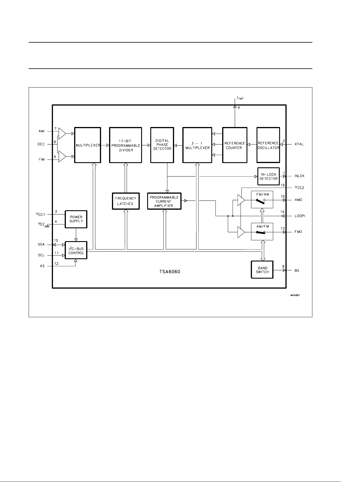
BLOCK DIAGRAM
TSA6060
Fig.1 Block diagram.
1995 Nov 23 3
Philips Semiconductors Product specification
Fast radio tuning PLL frequency
synthesizer
PINNING
SYMBOL PIN DESCRIPTION
INCLK 1 in-lock detector output
XTAL 2 crystal reference oscillator input
V
CC1
V
EE
FM
I
DEC 6 prescaler decoupling
AM
I
BS 8 band switch output
f
ref
SDA 10 serial data input (I
SCL 11 serial clock input (I
AS 12 address select input (I
FM
O
LOOP
I
AM
O
V
CC2
3 supply voltage (PLL supply 1)
4 ground
5 FM VCO input
7 AM VCO input
9 40 kHz reference output
2
C-bus)
2
C-bus)
2
C-bus)
13 FM output for external loop filter
14 tuning voltage amplifier input
15 AM output for external loop filter
16 supply voltage (PLL supply 2)
TSA6060
Fig.2 Pin configuration.
FUNCTIONAL DESCRIPTION
The TSA6060 contains the following parts:
• Separate input amplifiers for the AM and FM VCO
signals.
• A 17-bit programmable counter.
• A digital memory phase detector.
• A reference frequency channel which contains a 4 MHz
or 8 MHz crystal oscillator which is followed by a
reference counter. The reference frequency can be
either 1, 5, 10 or 50 kHz and is applied to the digital
memory phase detector. The reference counter can also
output a 40 kHz reference frequency to pin 9 for
communication between the FM/IF system and the
microcontroller-based tuning interface IC (TEA6100).
• A programmable current amplifier (charge pump) which
consists of a 25 mA and a 500 mA current source. This
allows adjustment of the loop gain thereby providing
high-current high-speed tuning and low-current stable
tuning.
• A one-input-two-output tuning voltage amplifier. One
output is connected to the external AM loop filter and the
other output to the external FM loop filter. Under
software control, the AM output is switched to a low
impedance to ground by the FM/AM switch in the FM
position. The FM output is switched to a low impedance
to ground by the AM/FM switch in the AM position. The
outputs can deliver a tuning voltage of up to 10.5 V.
2
C-bus interface with data latches and control logic.
• An I
The I2C-bus is intended for communication between
microcontrollers and different ICs or modules. Detailed
information concerning the I2C-bus specification is
available on request.
• A software controlled band switch output.
Controls
The TSA6060 is controlled via the 2-wire I
2
C-bus.
For programming there is one module address, a logic 0
(R/W bit) and four data bytes. The module address
contains an address select bit (AS) which enables two
TSA6060s to be operated in one system.
The auto-increment facility of the I2C-bus allows
programming of the TSA6060 within one transmission
(address + 4 data bytes).
The TSA6060 can also be partially programmed.
Transmission must then be ended by a STOP condition.
1995 Nov 23 4
Philips Semiconductors Product specification
Fast radio tuning PLL frequency
TSA6060
synthesizer
The bit organization of the 4 data bytes is shown in Fig.3. Further information is given in Tables 2, 3, 4 and 5.
The bits S0 to S16 (DB0: D7 to D1; DB1: D7 to D0; DB2: D1 to D0) together with bit FM/AM (DB2: D5) are used to set
the divider of the input frequency at inputs AMI (pin 7) or FMI (pin 5). If the system is in-lock the following is valid, as
shown in Table 1.
Table 1 System-in-lock (note 1).
FM/AM INPUT FREQUENCY (fi) INPUT
0
0 (S2 × 2
1 (S0 × 2
Note
1. The minimum dividing ratio for the AM mode is 2
Table 2 Bit CP is used to control the charge pump
current (DB0: D0).
CP CURRENT
0 LOW
1 HIGH
+S3×21..... + S15 × 213+ S16 × 214) × f
0
+S1×21..... + S15 × 215+ S16 × 216) × f
ref
ref
6
= 64 and for the FM mode is 28= 256.
Table 5 Bit BS controls the open-collector band switch
output (DB2: D2).
BS BAND SWITCH OUTPUT
1 sink current
0 floating
AM
FM
Table 3 Bits REF1 and REF2 are used to set the
reference frequency applied to the phase
detector (DB2: D7 to D6).
REF1 REF2
00 1
01 10
10 25
11 50
Table 4 Bit
FM/AM
OPERATIONAL
AMPLIFIER
FM/AM OPAMP controls the switch AM/FM,
FM/AM in the tuning voltage amplifier circuits
(DB2: D4).
1 closed open
0 open closed
FM/AM AM/FM
REFERENCE
FREQUENCY (kHZ)
SWITCH
The bit 8/4 MHz controls a divide-by-1/divide-by-2 divider
cell in the reference oscillator section. This allows the use
of a 4 MHz or 8 MHz crystal.
Table 6 Test mode.
T3 T2 T1 FUNCTION
0 X 0 normal
1 0 1 CP source
0 1 1 CP sink
1 1 1 CP 3-state
0 0 1 CP sink + source
1 1 X BS = main divider output
1 0 X BS = reference divider output
The data byte DB3 must be set to 0.....0. It is also used for
test purposes (see Fig.3)).
1995 Nov 23 5
 Loading...