

Philips tsa6057 DATASHEETS

INTEGRATED CIRCUITS
DATA SH EET
TSA6057
TSA6057T
Radio tuning PLL frequency
synthesizer
Product specification
File under Integrated Circuits, IC01
August 1988

Philips Semiconductors Product specification
Radio tuning PLL frequency synthesizer
FEA TURES
• On-chip AM and FM prescalers with high input
sensitivity
• On-chip high performance one input (two output) tuning
voltage amplifier for the AM and FM loop filters
• On-chip 2-level current amplifier (charge pump) to
adjust the loop gain
• Only one reference oscillator (4 MHz) for both AM and
FM
• High speed tuning due to a powerful digital memory
phase detector
• 40 kHz output reference frequency for co-operation with
the FM/IF system and microcomputer-based tuning
interface IC (TEA6100)
• Oscillator frequency ranges of: 512 kHz to 30 MHz and
30 MHz to 150 MHz
• Three selectable reference frequencies of 1 kHz, 10 kHz
or 25 kHz for both tuning ranges
• Serial 2-wire I2C-bus interface to a microcomputer and
one programmable address input
• Software controlled bandswitch output.
TSA6057
TSA6057T
GENERAL DESCRIPTION
The TSA6057/6057T is a bipolar single chip frequency
synthesizer manufactured in SUBILO-N technology
(components laterally separated by oxide). It performs all
the tuning functions of a PLL radio tuning system. The IC
is designed for application in all types of radio receivers.
PACKAGE OUTLINES
TSA6057: 16-lead DIL; plastic (SOT38);
SOT38-1; 1996 August 07.
TSA6057T: 16-lead minipack; plastic (SO16L; SOT162A);
SOT162-1; 1996 August 07.
QUICK REFERENCE DATA
PARAMETER CONDITIONS SYMBOL MIN. TYP. MAX. UNIT
Supply voltage
pin 3 V
pin 16 V
Supply current no outputs loaded
pin 3 I
pin 16 I
Max. input frequency on AM
Min. input frequency on AM
Max. input frequency on FM
Min. input frequency on FM
Input voltage on AM
I
l
l
I
I
V
= 0 V
iFM
(RMS value) V
V
Input voltage on FM
I
iAM
= 0 V
(RMS value) V
Total power dissipation P
Operating ambient
temperature range T
CC1
CC2
3
16
f
iAM
f
iAM
f
iFM
f
iFM
iAM(rms)
iFM(rms)
tot
amb
= V
3-4
= V
16-4VCC1
4.5 5.0 5.5 V
8.5 12 V
12 20 28 mA
0.7 1.0 1.3 mA
30 −−MHz
−−0.512 MHz
150 −−MHz
−−30 MHz
30 − 500 mV
20 − 300 mV
− 0.14 − W
−30 −+ 85 °C
August 1988 2
Philips Semiconductors Product specification
Radio tuning PLL frequency synthesizer
TSA6057
TSA6057T
August 1988 3
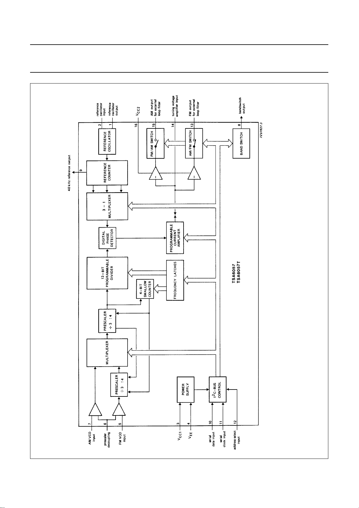
Fig.1 Block diagram.
Philips Semiconductors Product specification
Radio tuning PLL frequency synthesizer
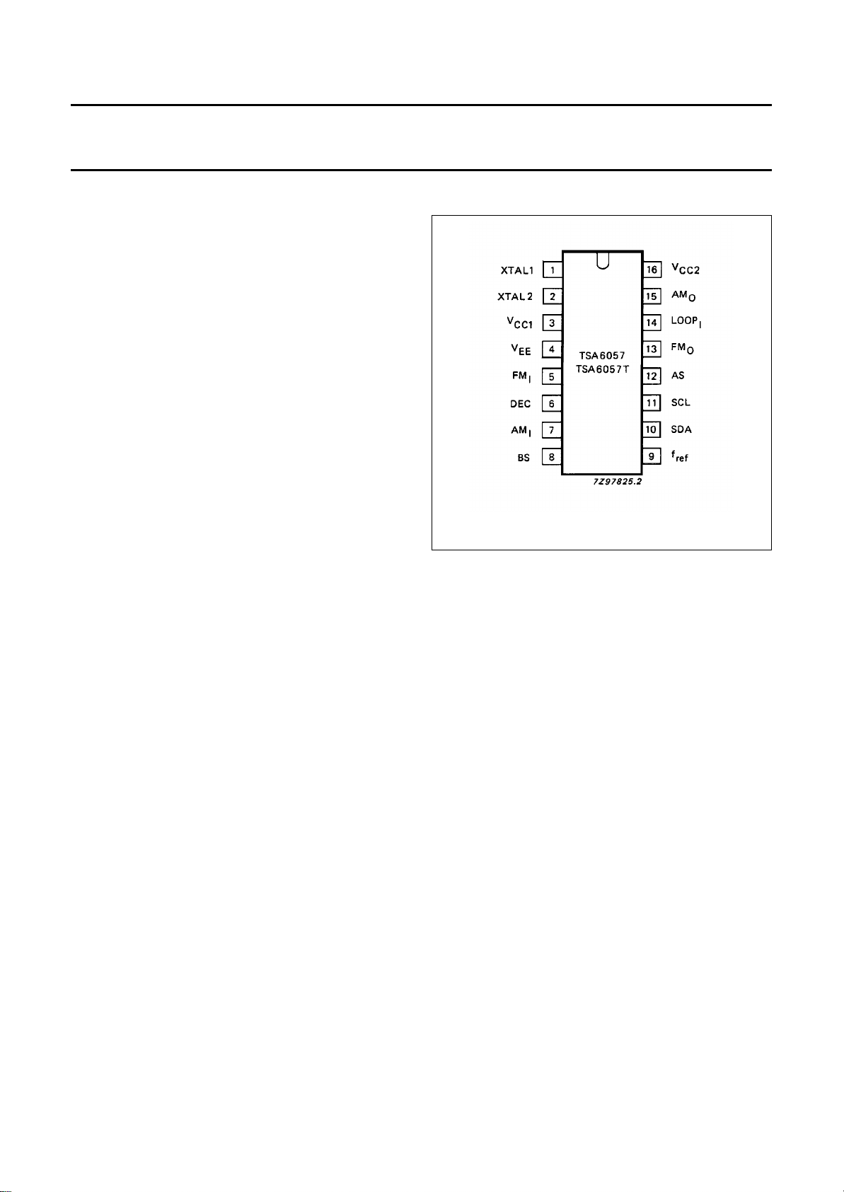
PINNING
1 XTAL1 reference oscillator output
2 XTAL2 reference oscillator input
3V
CC1
4V
EE
5FM
6 DEC prescaler decoupling
7AM
8 BS bandswitch output
9f
ref
10 SDA serial data input; I
11 SCL serial clock input; I
12 AS address select input; I
13 FM
14 LOOP
15 AM
16 V
CC2
positive supply voltage
ground
FM VCO input
I
AM VCO input
I
40 kHz reference output
FM output for external loop filter
O
tuning voltage amplifier input
I
AM output for external loop filter
O
positive supply voltage
2
C-bus
2
C-bus
2
C-bus
TSA6057
TSA6057T
Fig.2 Pinning diagram.
FUNCTIONAL DESCRIPTION
The TSA6057/6057T contains the following parts and facilities:
• Separate input amplifiers for the AM and FM VCO-signals.
• A prescaler with the divisors 3:4 on AM and 15:16 on FM, a multiplexer to select AM or FM and a 4-bit programmable
swallow counter.
• A 13-bit programmable counter.
• A digital memory phase detector.
• A reference frequency channel comprised of a 4 MHz crystal oscillator followed by a reference counter. The reference
frequency can be 1 kHz, 10 kHz or 25 kHz and is applied to the digital memory phase detector. The reference counter
also outputs a 40 kHz reference frequency to pin 9 for co-operation with the FM/IF system and microcomputer-based
tuning interface IC (TEA6100).
• A programmable current amplifier (charge pump) which consists of a 5 µA and a 450 µA current source. This allows
adjustment of loop gain, thus providing high current-high speed tuning and low current-stable tuning.
• A one input − two output tuning voltage amplifier. One output is connected to the external AM loop filter and the other
output to the external FM loop filter. Under software control, the AM output is switched to a high impedance state by
the FM/AM switch in the FM position and the FM output is switched to a high impedance state by the AM/FM switch in
the AM position. The outputs can deliver a tuning voltage of up to 10.5 V.
• An I2C-bus interface with data latches and control logic. The I2C-bus is intended for communication between
microcontrollers and different ICs or modules. Detailed information on the I2C-bus specification is available on request.
• A software-controlled bandswitch output.
August 1988 4

Philips Semiconductors Product specification
Radio tuning PLL frequency synthesizer
TSA6057
TSA6057T
Controls
The TSA6057/6057T is controlled via the 2-wire I2C-bus. For programming there is one module address, a logic 0 R/W
bit, a subaddress byte and four data bytes. The subaddress determines which one of the four data bytes is transmitted
first. The module address contains a programmable address bit (D1) which with address select input AS (pin 12) makes
it possible to operate two TSA6057s in one system.
The auto increment facility of the I2C-bus allows programming of the TSA6057/6057T within one transmission
(address + subaddress + 4 data bytes).
• The TSA6057/6057T can also be partially programmed. Transmission must then be ended by a stop condition.
The bit organization of the 4 data bytes is shown in Fig.3 and are described in sections (a) to (f).
(a) The bits S0 to S16 (DB0: D7-D1; DB1: D7-D0; DB2: D1-D0) together with bit FM/AM (DB2: D5) are used to set the
divisor of the input frequency at inputs AMI (pin 7) or FMI (pin 5). If the system is in lock the following is valid:
FM/AM INPUT FREQUENCY (FI) INPUT
0
0 (S0 × 2
1 (S0 × 20+ S1 × 21..... + S15 × 215+ S16 × 216) × f
Where
The minimum dividing ratio for AM mode is 2
The minimum dividing ratio for FM mode is 28 = 256
+ S1 × 21..... + S13 × 213+ S14 × 214) × f
6
= 64
ref
ref
AM
FM
l
I
(b) The bit CP is used to control the charge pump current (DB0: D0).
CP CURRENT
0 low
1 high
(c) The bits REF1 and REF2 are used to set the reference frequency applied to the phase detector (DB2: D7-D6).
REF1 REF2
00 1
01 10
10 25
1 1 none
(d) The bit
FM/AM OPAMP SWITCH FM/AM SWITCH AM/FM
1 closed open
0 open closed
FM/AM OPAMP controls the switch AM/FM; FM/AM in the tuning voltage amplifier output circuitry (DB2: D4).
FREQUENCY
(kHZ)
August 1988 5
 Loading...