

Philips TSA5527M-C1, TSA5527AM-C2, TSA5526T-C2-M1, TSA5526T-C2, TSA5526T-C1-M1 Datasheet
...
DATA SH EET
Product specification
Supersedes data of 1995 Mar 22
File under Integrated Circuits, IC02
1996 Sep 24
INTEGRATED CIRCUITS
TSA5526; TSA5527
1.3 GHz universal bus-controlled
TV synthesizers
1996 Sep 24 2
Philips Semiconductors Product specification
1.3 GHz universal bus-controlled
TV synthesizers
TSA5526; TSA5527
FEATURES
• Complete 1.3 GHz single chip system
• Four PNP band switch buffers (40 mA)
• 33 V output tuning voltage
• In-lock detector
• 5-step ADC
• 15-bit programmable divider
• Programmable reference divider ratio
(512, 640 or 1024)
• Programmable charge-pump current (60 or 280 µA)
• Programmable automatic charge-pump current switch
• Varicap drive disable
• Universal bus protocol I
2
C-bus or 3-wire bus:
– bus protocol for 18 or 19 bits transmission
(3-wire bus)
– extra protocol for 27 bits for test and features
(3-wire bus)
– address plus 4 data bytes transmission (I2C-bus write
mode)
– address plus 1 status byte transmission (I2C-bus
read mode)
– three independent I2C-bus addresses
• Low power and low radiation.
APPLICATIONS
• TV tuners and front ends
• VCR tuners.
ORDERING INFORMATION
TYPE NUMBER
PACKAGE
NAME DESCRIPTION VERSION
TSA5526M SSOP16 plastic shrink small outline package; 16 leads; body width 4.4 mm SOT369-1
TSA5526T SO16 plastic small outline package; 16 leads; body width 3.9 mm SOT109-1
TSA5527M SSOP16 plastic shrink small outline package; 16 leads; body width 4.4 mm SOT369-1
TSA5527T SO16 plastic small outline package; 16 leads; body width 3.9 mm SOT109-1
TSA5526AM SSOP16 plastic shrink small outline package; 16 leads; body width 4.4 mm SOT369-1
TSA5526AT SO16 plastic small outline package; 16 leads; body width 3.9 mm SOT109-1
TSA5527AM SSOP16 plastic shrink small outline package; 16 leads; body width 4.4 mm SOT369-1
TSA5527AT SO16 plastic small outline package; 16 leads; body width 3.9 mm SOT109-1
1996 Sep 24 3
Philips Semiconductors Product specification
1.3 GHz universal bus-controlled
TV synthesizers
TSA5526; TSA5527
QUICK REFERENCE DATA
Notes
1. One band switch buffer ON, I
o
= 40 mA.
2. One band switch buffer ON, Io= 40 mA; two buffers ON, maximum sum of Io=50mA.
3. The power dissipation is calculated as follows:
kΩ.
SYMBOL PARAMETER CONDITIONS MIN. TYP. MAX. UNIT
V
CC1
supply voltage (+5 V) 4.5 − 5.5 V
V
CC2
band switch supply voltage (12 V) V
CC1
12 13.5 V
I
CC1
supply current − 20 25 mA
I
CC2
band switch supply current note 1 − 50 55 mA
f
RF
RF input frequency 64 − 1300 MHz
V
i(RF)
RF input voltage fi= 80 to 150 MHz −25 − 3 dBm
f
i
= 150 to 1000 MHz −28 − 3 dBm
f
i
= 1000 to 1300 MHz −15 − 3 dBm
f
xtal
crystal oscillator input frequency 3.2 4.0 4.48 MHz
I
o(PNP)
PNP band switch buffers output
current
note 2 4 − 50 mA
P
tot
total power dissipation note 3 − 250 400 mW
T
stg
storage temperature −40 − +150 °C
T
amb
operating ambient temperature −20 − +85 °C
P
D
V
CC1ICC1VCC2ICC2Io
–()I
o
V
CE satPNP()
V33 2⁄()
2
27⁄+×+×+×=
1996 Sep 24 4
Philips Semiconductors Product specification
1.3 GHz universal bus-controlled
TV synthesizers
TSA5526; TSA5527
GENERAL DESCRIPTION
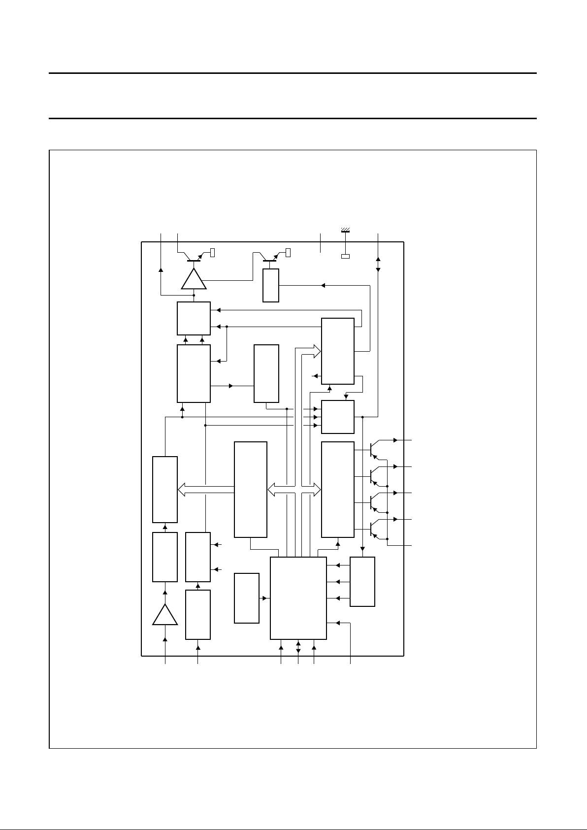
The device is a single-chip PLL frequency synthesizer
designed for TV and VCR tuning systems. The circuit
consists of a divide-by-eight prescaler with its own
preamplifier, a 15-bit programmable divider, a crystal
oscillator and its programmable reference divider and a
phase/frequency detector combined with a charge-pump
which drives the tuning amplifier and the 33 V output.
Four high-current PNP band switch buffers are provided
for band switching. Two PNP buffers can be switched on
simultaneously. The sum of the collector currents is limited
to 50 mA.
Depending on the reference divider ratio (512, 640 or
1024), the phase comparator operates at 3.90625 kHz,
6.25 kHz or 7.8125 kHz using a 4 MHz crystal.
The device can be controlled in accordance with the
I
2
C-bus format or the 3-wire bus format depending on the
voltage applied to the SW input (see Table 2). In the 3-wire
bus mode (SW = HIGH) pin 12 is the LOCK output.
The lock output is LOW when the PLL loop is locked. In the
I2C-bus mode (SW = LOW) the LOCK detector bit FL is set
to logic 1 when the loop is locked and is read on the SDA
line (status byte) during a read operation. The ADC input
is available on pin 12 for AFC control in the I2C-bus mode
only. The ADC code is read during a read operation on the
I2C-bus. In the test mode pin 12 is used as a test output for
f
ref
and1⁄2f
div
in the I2C-bus mode and the 3-wire bus mode
(see Table 6).
When the automatic charge-pump current switch mode is
activated, depending on the device given in Table 6, and
when the loop is phase-locked, the charge-pump current
value is automatically switched to LOW.
This action is taken to improve the carrier-to-noise ratio.
The status of this feature can be read in the ACPS flag
during a read operation on the I
2
C-bus (see Table 8).
I
2
C-bus format (SW = LOW)
Five serial bytes (including address byte) are required to
address the device, select the VCO frequency, program
the four PNP band switch buffers, set the charge-pump
current and the reference divider ratio.
The device has three independent I2C-bus addresses
which can be selected by applying a specific voltage on the
CE input (see Table 5). The general address C2 is always
valid. When the I2C-bus format is fully used, TSA5526 and
TSA5527 are equal.
3-wire bus format (SW = V
CC1
or open-circuit)
Data is transmitted to the device during a HIGH level on
the CE input (enable line pin 15). The device is compatible
with 18-bit and 19-bit data formats. The first four bits are
used to program the PNP band switch buffers and the
remaining bits are used to control the programmable
divider. A 27-bit data format may also be used to set the
charge-pump current, the reference divider ratio and for
test purposes. The differences between TSA5526 and
TSA5527 are given in Table 1.
When the 27-bit format is used, the TSA5526 and
TSA5527 are equal and the reference divider is controlled
by the RSA and RSB bits (see Table 7 and
Figs 3, 4 and 5).
Table 1 Differences between TSA5526 and TSA5527
Notes
1. The selection of the reference divider is given by an automatic identification of the data word length.
2. The reference divider is set to 640 at power-on reset.
TYPE NUMBER DATA WORD REFERENCE DIVIDER FREQUENCY STEP (kHz)
TSA5526 18-bit 512
(1)
62.5
TSA5526 19-bit 1024
(1)
31.25
TSA5527 19-bit 640
(2)
50
1996 Sep 24 5
Philips Semiconductors Product specification
1.3 GHz universal bus-controlled
TV synthesizers
TSA5526; TSA5527
BLOCK DIAGRAM
Fig.1 Block diagram.
handbook, full pagewidth
MBE327
8
BS1
7
BS2
6
BS3
5
BS4
4-BIT BAND SWITCH
REGISTER
GATE
7-BIT CONTROL
REGISTER
15-BIT FREQUENCY
REGISTER
IN-LOCK
DETECTOR
lock
DIGITAL
PHASE
COMPARATOR
RSA,RSB
T2,T1,T0
5-LEVEL
ADC
11
15
14
13
SCL
SDA
CE
I C/3-WIRE BUS
TRANSCEIVER
2
T2,T1,T0
AMP
CHARGE
PUMP
9
10
LOGIC
V
CC1
V
EE
3
2
12
LOCK/
ADC
4
V
CC2
SW
POWER-ON
RESET
XTAL
OSCILLATOR
DIVIDER
512/640/1024
RSA RSB
XTAL
16
OS
CP
CP
PRESCALER
DIVIDE-BY-8
1
RF
15-BIT
PROGRAMMABLE
DIVIDER
f
div
f
ref
TSA5526
TSA5527
V
tune
1996 Sep 24 6
Philips Semiconductors Product specification
1.3 GHz universal bus-controlled
TV synthesizers
TSA5526; TSA5527
PINNING
SYMBOL PIN DESCRIPTION
RF 1 RF signal input
V
EE
2 ground
V
CC1
3 supply voltage (+5 V)
V
CC2
4 band switch supply voltage (+12 V)
BS4 5 PNP band switch buffer output 4
BS3 6 PNP band switch buffer output 3
BS2 7 PNP band switch buffer output 2
BS1 8 PNP band switch buffer output 1
CP 9 charge-pump output
V
tune
10 tuning voltage output
SW 11 bus format selection input, I
2
C-bus
or 3-wire
LOCK/ADC 12 lock detector output (3-wire bus/
ADC input (I
2
C-bus)
SCL 13 serial clock input
SDA 14 serial data input/output
CE 15 chip enable/address selection input
XTAL 16 crystal oscillator input
Fig.2 Pin configuration.
handbook, halfpage
TSA5526
TSA5527
MBE326
1
2
3
4
5
6
7
8
16
15
14
13
12
11
10
9
RF
V
V
V
BS4
BS3
BS2
BS1
CP
SW
LOCK/ADC
SCL
SDA
CE
XTAL
EE
CC1
CC2
V
tune
FUNCTIONAL DESCRIPTION
The device is controlled via the I2C-bus or the 3-wire bus
depending on the voltage applied to the SW input (pin 11).
A HIGH level on the SW input enables the 3-wire bus
inputs which are CE (Chip Enable), SDA (serial data input)
and SCL (serial clock input). A LOW level on the SW input
enables the I2C-bus inputs which are AS (Address
Selection input), SDA (serial data input/output) and SCL
(serial clock input). The bus format selection is given in
Table 2.
I
2
C-bus mode (SW = LOW); see Table 3
W
RITE MODE (R/W = 0)
Data bytes can be sent to the device after the address
transmission (first byte). Four data bytes are required to
fully program the device. The bus transceiver has an
auto-increment facility which permits the programming of
the device within one single transmission
(address + 4 data bytes).
The device can also be partially programmed providing
that the first data byte following the address is Divider
Byte 1 (DB1) or the Control Byte (CB). The bits in the data
bytes are defined in Table 3.
The first bit of the first data byte transmitted indicates
whether frequency data (first bit = logic 0) or control and
band switch data (first bit = logic 1) will follow. Until an
I
2
C-bus STOP command is sent by the controller,
additional data bytes can be entered without the need to
readdress the device. The frequency register is loaded
after the 8th clock pulse of the second Divider Byte (DB2),
the control register is loaded after the 8th clock pulse of the
Control Byte (CB) and the band switch register is loaded
after the 8th clock pulse of the Band switch Byte (BB).
I
2
C-BUS ADDRESS SELECTION
The module address contains programmable address bits
(MA1 and MA0) which offer the possibility of having
several synthesizers (up to 3) in one system by applying a
specific voltage to the CE input.
The relationship between MA1 and MA0 and the input
voltage applied to the CE input is given in Table 5.
1996 Sep 24 7
Philips Semiconductors Product specification
1.3 GHz universal bus-controlled
TV synthesizers
TSA5526; TSA5527
Table 2 Bus format selection
Table 3 I
2
C-bus data format
Table 4 Description of Table 3
Table 5 I
2
C-bus address selection
PIN NAME 3-WIRE BUS MODE I
2
C-BUS MODE
11 SW OPEN or HIGH LOW
12 LOCK/ADC LOCK/TEST output ADC input/TEST output
13 SCL clock input SCL input
14 SDA data input SDA input/output
15 CE chip enable input address selection input
BYTE MSB DATA BYTE LSB
SLAVE
ANSWER
Address Byte (ADB) 1 1000MA1MA0R/W=0 A
Divider Byte 1 (DB1) 0 N14 N13 N12 N11 N10 N9 N8 A
Divider Byte 2 (DB2) N7 N6 N5 N4 N3 N2 N1 N0 A
Control Byte (CB) 1 CP T2 T1 T0 RSA RSB OS A
Band switch Byte (BB) X X X X BS4 BS3 BS2 BS1 A
SYMBOL DESCRIPTION
A acknowledge
MA1 and MA0 programmable address bits (see Table 5)
N14 to N0 programmable divider bits; N = N14 × 2
14
+ N13 × 213+...+N1×2+N0
CP charge-pump current; CP = 0 = 60 µA; CP = 1 = 280 µA (default)
T2 to T0 test bits (see Table 6); for normal operation T2 = 0, T1 = 0 and T0 = 1 (default)
RSA and RSB reference divider ratio select bits (see Table 7)
OS tuning amplifier control bit; for normal operation OS = 0 and tuning voltage is ON (default);
when OS = 1 tuning voltage is OFF (high impedance)
BS4 to BS1 PNP band switch buffers control bits; when BS
n
= 0 buffer n is OFF; when BSn= 1 buffer n
is ON
X don’t care
VOLTAGE APPLIED TO THE CE INPUT (SW = LOW) MA1 MA0
0 V to 0.1V
CC1
00
Always valid 0 1
0.4V
CC1
to 0.6V
CC1
10
0.9V
CC1
to V
CC1
11
1996 Sep 24 8
Philips Semiconductors Product specification
1.3 GHz universal bus-controlled
TV synthesizers
TSA5526; TSA5527
Table 6 Test bits
T2 T1 T0 TSA5526; TSA5527 TSA5526A; TSA5527A REMARKS
0 0 0 normal operation with automatic
charge-pump switch ON
automatic charge-pump switch OFF
0 0 1 normal operation with automatic
charge-pump switch OFF
automatic charge-pump switch ON status at POR
0 1 X charge-pump is OFF charge-pump is OFF
1 1 0 charge-pump is sinking current charge-pump is sinking current
1 1 1 charge-pump is sourcing current charge-pump is sourcing current
100f
ref
is available at LOCK output f
ref
is available at LOCK output the ADC cannot be used
when test mode is active
101
1
⁄2f
div
is available at LOCK output
1
⁄2f
div
is available at LOCK output the ADC cannot be used
when test mode is active
Table 7 Ratio select bits
R
EAD MODE (R/W = LOGIC 1); see Table 8
Data can be read from the device by setting the R/W bit to
logic 1. After the slave address has been recognized, the
device generates an acknowledge pulse and the first data
byte (status byte) is transferred on the SDA line (MSB
first). Data is valid on the SDA line during a HIGH level of
the SCL clock signal. A second data byte can be read from
the device if the microcontroller generates an
acknowledge on the SDA line (master acknowledge).
End of transmission will occur if no master acknowledge
occurs.
RSA RSB REFERENCE DIVIDER
X 0 640
0 1 1024
1 1 512
The device will then release the data line to allow the
microcontroller to generate a stop condition. The POR flag
is set to logic 1 at power-on. The flag is reset when an
end-of-data is detected by the device (end of a read
sequence). Control of the loop is made possible with the
in-lock flag (FL) which indicates when the loop is locked
(FL = logic 1).
The Automatic Charge-Pump Switch flag (ACPS) is LOW
when the automatic charge-pump switch mode is ON and
the loop is locked. In other conditions ACPS = logic 1.
When ACPS = logic 0, the charge-pump current is forced
to the LOW value.
A built-in ADC is available at pin 12 (I2C-bus only).
This converter can be used to apply AFC information to the
microcontroller from the IF section of the television.
The relationship between the bits A2 to A0 is given in
Table 9.
Table 8 Read data format
Notes
1. A = acknowledge.
2. POR = power-on reset flag (POR = logic 1 at power-on).
3. FL = in-lock flag (FL = logic 1 when the loop is locked).
4. ACPS = automatic charge-pump switch flag (active ACPS = logic 0; non-active ACPS = logic 1).
5. A2 to A0 = digital outputs of the 5-level ADC.
BYTE MSB DATA BYTE LSB
SLAVE
ANSWER
Address Byte (ADB) 1 1 0 0 0 MA1 MA0 R/W = 1 A
(1)
Status Byte (SB) POR
(2)
FL
(3)
ACPS
(4)
11A2
(5)
A1
(5)
A0
(5)
−
1996 Sep 24 9
Philips Semiconductors Product specification
1.3 GHz universal bus-controlled
TV synthesizers
TSA5526; TSA5527
Table 9 ADC levels
Note
1. Accuracy is ±0.03V
CC1
.
3-wire bus mode (SW = open-circuit or V
CC1
);
see Figs 3, 4 and 5
During a HIGH level on the CE input, the data is clocked
into the data register at the HIGH-to-LOW transition of the
clock pulse. The first four bits control the band switch
buffers and are loaded into the internal band switch
register on the 5th rising edge of the clock pulse.
The frequency bits are loaded into the frequency register
at the HIGH-to-LOW transition of the chip enable line when
an 18-bit or 19-bit data word is transmitted.
At power-on the charge-pump current is set to 280 µA, the
tuning voltage output is disabled (V
tune
= 33 V in
VOLTAGE APPLIED
AT ADC INPUT
(1)
A2 A1 A0
0.6V
CC1
to V
CC1
100
0.45V
CC1
to 0.6V
CC1
011
0.3V
CC1
to 0.45V
CC1
010
0.15V
CC1
to 0.3V
CC1
001
0 to 0.15V
CC1
000
application; see Fig.12), the test bits T2, T1 and T0 are set
to the 0 0 1 state in the normal mode with ACPS OFF for
TSA55226; TSA5527 and ACPS ON for TSA5526A;
TSA5527A. RSB is set to logic 1 (TSA5526) or logic 0
(TSA5527). When an 18-bit data word is transmitted, the
most significant bit of the divider N14 is internally set to
logic 0 and bit RSA is set to logic 1. When a 19-bit data
word is transmitted, bit RSA is set to logic 0.
When a 27-bit word is transmitted, the frequency bits are
loaded into the frequency register on the 20th rising edge
of the clock pulse and the control bits at the HIGH-to-LOW
transition of the chip enable line. In this mode, the
reference divider is given by the RSA and RSB bits
(see Table 7). The test bits T2, T1 and T0, the
charge-pump bit CP, the ratio select bit RSB and the
OS bit can only be selected or changed with a 27-bit
transmission. They remain programmed if an 18-bit or a
19-bit transmission occurs. Only RSA is controlled by the
transmission length when the 18-bit or 19-bit format is
used.
A data word of less than 18 bits will not affect the
frequency register of the device. The definition of the bits
is unchanged compared to the I2C-bus mode.
The power-on detection threshold voltage V
POR
is fixed to
V
CC1
= 2 V at room temperature. Below this threshold, the
device is reset to the power-on state previously described.
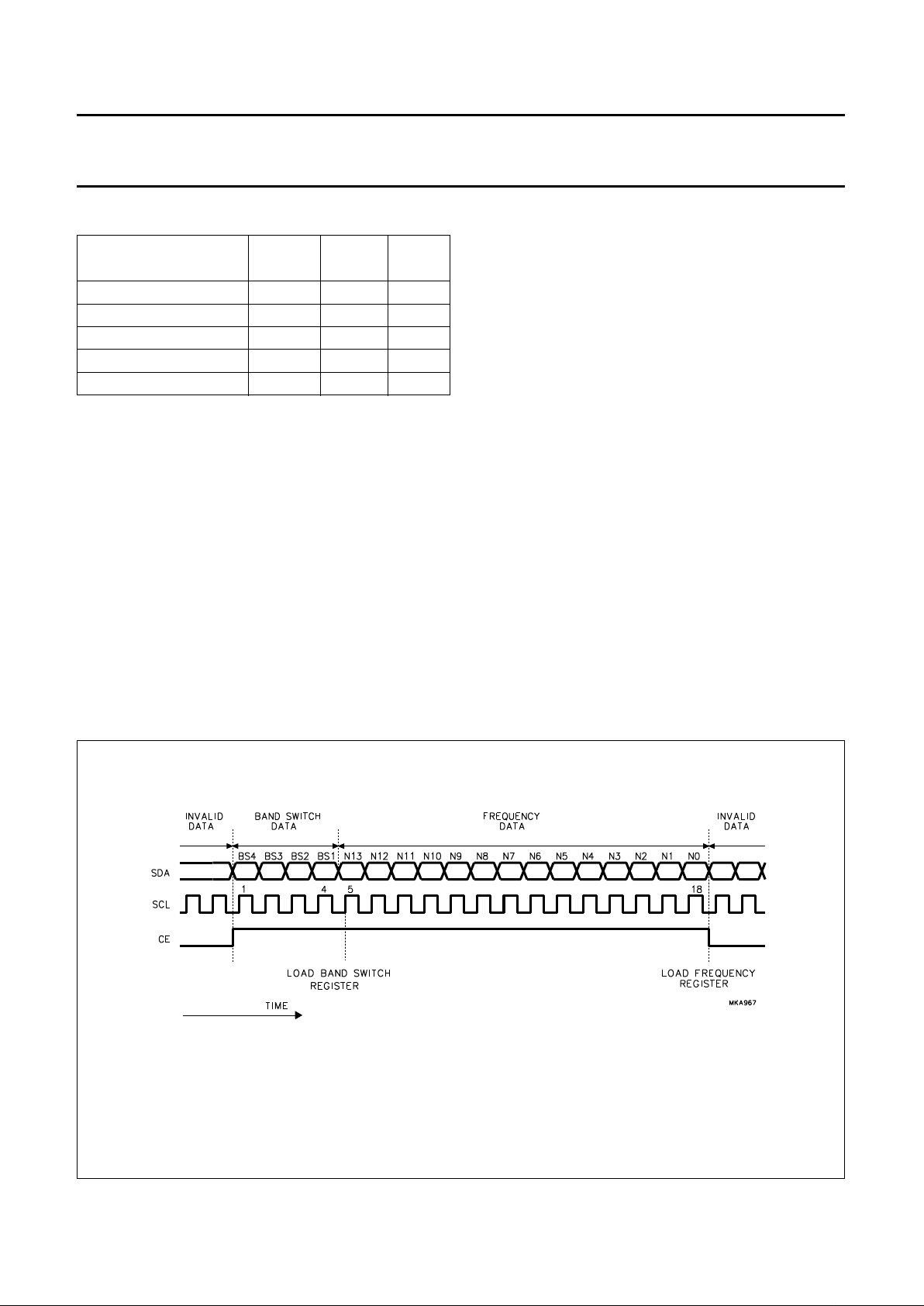
Fig.3 Normal mode; 18-bit data format (RSA = 1).
For TSA5526 bit RSB =logic 1 at power-on; the reference divider is 512 or 1024.
For TSA5527 bit RSB =logic 0 at power-on; the reference divider is 640.
For TSA5526 and TSA5527 the value of RSB can also be programmed by using the 27-bit data format. When returning to the normal mode, bit RSB
remains as programmed with the 27-bit data word.
 Loading...