

Philips TSA5522T-C1 Datasheet

DATA SH EET
Product specification
Supersedes data of 1995 Mar 22
File under Integrated Circuits, IC02
1996 Jan 23
INTEGRATED CIRCUITS
TSA5522
1.4 GHz I
2
C-bus controlled
synthesizer
1996 Jan 23 2
Philips Semiconductors Product specification
1.4 GHz I2C-bus controlled synthesizer
TSA5522
FEATURES
• Complete 1.4 GHz single chip system
• Three PNP band switch buffers (20 mA)
• Four bus-controlled bidirectional ports (NPN
open-collector outputs); only one port in 16-pin version
• 33 V tuning voltage output
• In-lock detector
• 5-step ADC
• Mixer-Oscillator (M/O) band switch output
• 15-bit programmable divider
• Programmable reference divider ratio (512, 640
or 1024)
• Programmable charge-pump current (50 or 250 µA)
• Varicap drive disable
• I
2
C-bus format
– address plus 4 data bytes transmission (write mode)
– address plus 1 status byte transmission (read mode)
– three independent addresses
• Low power and low radiation.
APPLICATIONS
• TV tuners and front-ends
• VCR tuners.
ORDERING INFORMATION
TYPE NUMBER
PACKAGE
NAME DESCRIPTION VERSION
TSA5522M SSOP20 plastic shrink small outline package; 20 leads; body width 4.4 mm SOT266-1
TSA5522T SO16 plastic small outline package; 16 leads; body width 3.9 mm SOT109-1
1996 Jan 23 3
Philips Semiconductors Product specification
1.4 GHz I2C-bus controlled synthesizer
TSA5522
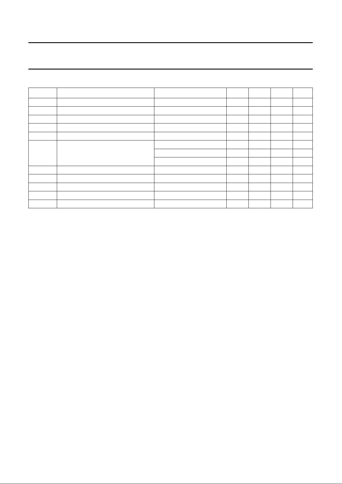
QUICK REFERENCE DATA
Note
1. One band switch buffer ON; I
o
= 20 mA.
SYMBOL PARAMETER CONDITIONS MIN. TYP. MAX. UNIT
V
CC1
supply voltage (+5 V) 4.5 − 5.5 V
V
CC2
band switch supply voltage (+12 V) V
CC1
12 13.5 V
I
CC1
supply current − 22 30 mA
I
CC2
band switch supply current note 1 − 27 32 mA
f
RF
RF input frequency 64 − 1400 MHz
V
i(RF)
RF input voltage fi= 80 to 150 MHz − 25 − 3 dBm
f
i
= 150 to 1000 MHz − 28 − 3 dBm
f
i
= 1000 to 1400 MHz − 26 − 3 dBm
f
xtal
crystal oscillator input frequency − 4 − MHz
I
o(PNP)
PNP band switch buffers output current − 20 25 mA
I
o(NPN)
NPN open-collector output current − 20 25 mA
T
amb
operating ambient temperature −20 − +85 °C
T
stg
storage temperature (IC) −40 − +150 °C
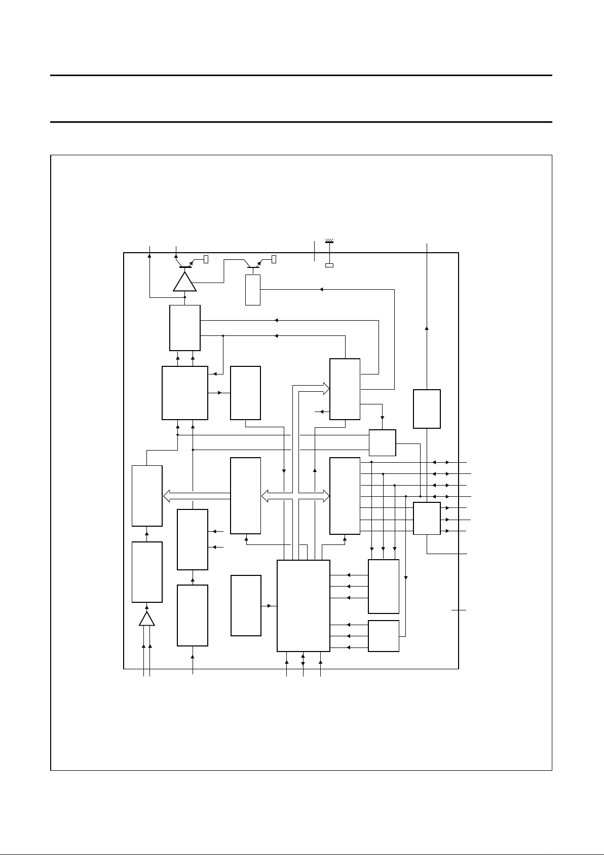
GENERAL DESCRIPTION (see Fig.1)
The device is a single chip PLL frequency synthesizer
designed for TV and VCR tuning systems. The circuit
consists of a divide-by-eight prescaler with its own
preamplifier, a 15-bit programmable divider, a crystal
oscillator and its programmable reference divider and a
phase/frequency detector combined with a charge-pump
which drives the tuning amplifier, including 33 V output.
Three high-current PNP band switch buffers are provided
for band switching together with four open-collector NPN
outputs (only one open-collector output on 16-pin
devices). These ports can also be used as input ports [one
Analog-to Digital Converter (ADC) and three general
purpose I/O ports (not available on 16-pin devices)]. An
output is provided to control a Philips mixer/oscillator IC in
combination with the PNP buffers state.
Depending on the reference divider ratio (512, 640
or 1024), the phase comparator operates at 3.90625 kHz,
6.25 kHz or 7.8125 kHz with a 4 MHz crystal. The LOCK
detector bit FL is set to logic 1 when the loop is locked and
is read on the SDA line (status byte) during a read
operation.
The ADC is available for digital AFC control. The ADC
code is read during a read operation on the I
2
C-bus. The
ADC input is combined with the port P6. In the TEST
mode, this port is also used as a TEST output for f
ref
and
1
⁄2f
div
(see Table 4).
I
2
C-bus format
Five serial bytes (including address byte) are required to
address the device, select the VCO frequency, program
the ports, set the charge-pump current and the reference
divider ratio. The device has three independent I2C-bus
addresses selected by applying a specific voltage on AS
input (see Table 3). The general address C2 is always
valid.
1996 Jan 23 4
Philips Semiconductors Product specification
1.4 GHz I2C-bus controlled synthesizer
TSA5522
BLOCK DIAGRAM
Fig.1 Block diagram (SSOP20).
handbook, full pagewidth
PRESCALER
DIVIDE-BY-8
DIVIDER
512/640/1024
XTAL
OSCILLATOR
POWER-ON
RESET
15-BIT
PROGRAMMABLE
DIVIDER
15-BIT
FREQUENCY
REGISTER
7-BIT PORTS
REGISTER
7-BIT CONTROL
REGISTER
DIGITAL
PHASE
COMPARATOR
IN-LOCK
DETECTOR
CHARGE
PUMP
I C -BUS
TRANSCEIVER
2
ADC COMPARATORS
PNP
BUFFERS
BAND
SWITCH
P0n.c. V
P1
P2
P6
P4
P5
P7
LOGIC
OS
CP
BS
CC1
V
GATE
RSA RSB
RSA,RSB
67 10 9 8 13161514
2
3
28
17
SCL
SDA
AS
18
19
XTAL
RF2
RF1
ref
div
11
CP
12
1
5
4
T2,T1,T0
T2,T1,T0
EE
LOCK
TSA5522
MLD226
CC2
V
f
f
AMP
V
tune
1996 Jan 23 5
Philips Semiconductors Product specification
1.4 GHz I2C-bus controlled synthesizer
TSA5522
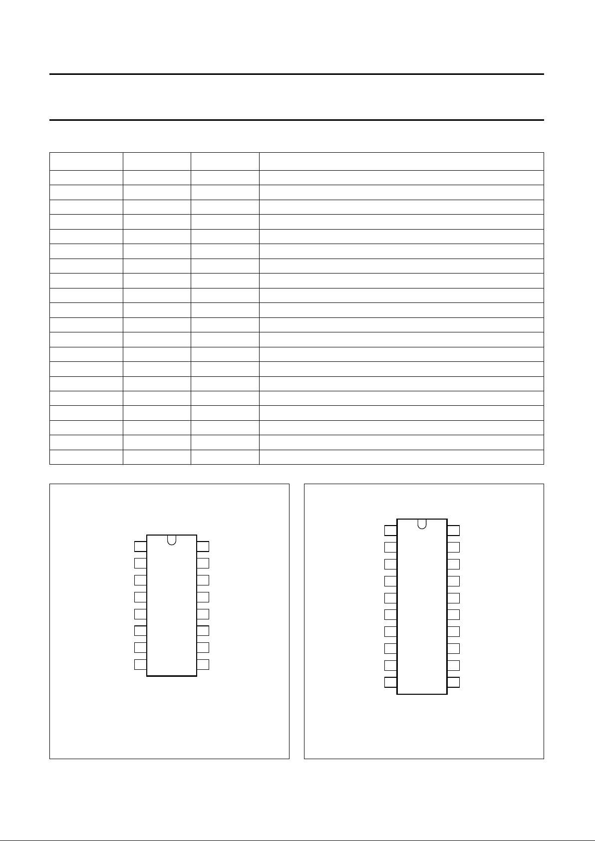
PINNING
SYMBOL SO16 SSOP20 DESCRIPTION
V
CC1
1 1 voltage supply (+5 V)
RF1 2 2 RF signal input 1
RF2 3 3 RF signal input 2
BS 4 4 band switch output to mixer/oscillator drive
V
EE
5 5 ground
V
CC2
6 6 voltage supply (+12 V)
n.c. − 7 not connected
P2 7 8 PNP band switch buffer output 2
P1 8 9 PNP band switch buffer output 1
P0 9 10 PNP band switch buffer output 0
CP 10 11 charge-pump output
V
tune
11 12 tuning voltage output
P6 12 13 NPN open-collector output/ADC input
P7 − 14 NPN open-collector output/comparator input
P5 − 15 NPN open-collector output/comparator input
P4 − 16 NPN open-collector output/comparator input
SCL 13 17 serial clock input
SDA 14 18 serial data input/output
AS 15 19 address selection input
XTAL 16 20 crystal oscillator input
Fig.2 Pin configuration (SO16).
handbook, halfpage
MLD225
TSA5522T
1
2
3
4
5
6
7
8
16
15
14
13
12
11
10
9
V
RF1
RF2
BS
V
P2
P1
EE
XTAL
AS
SDA
SCL
V
CP
PO
P6
CC1
V
CC2
tune
Fig.3 Pin configuration (SSOP20).
handbook, halfpage
TSA5522M
MLD230
1
2
3
4
5
6
7
8
9
10
20
19
18
17
16
15
14
13
12
11
XTAL
AS
SDA
SCL
P4
P5
P7
P6
CP
RF1
RF2
BS
CC2
V
CC1
V
EE
V
n.c.
P2
P1
P0
V
tune
1996 Jan 23 6
Philips Semiconductors Product specification
1.4 GHz I2C-bus controlled synthesizer
TSA5522
FUNCTIONAL DESCRIPTION
The device is controlled via the two-wire I2C-bus. For
programming, there is one module address (7 bits) and the
R/W bit for selecting the READ or the WRITE mode.
I
2
C-bus mode
W
RITE MODE (R/W = 0); see Table 1
Data bytes can be sent to the device after the address
transmission (first byte). Four data bytes are required to
fully program the device. The bus transceiver has an
auto-increment facility which permits the programming of
the device within one single transmission
(address + 4 data bytes).
The device can also be partially programmed providing
that the first data byte following the address is divider
byte 1 (DB1) or control byte (CB). The bits in the data
bytes are defined in Table 1. The first bit of the first data
byte transmitted indicates whether frequency data
(first bit = 0) or control and ports data (first bit = 1) will
follow. Until an I
2
C-bus STOP command is sent by the
controller, additional data bytes can be entered without the
need to re-address the device. The frequency register is
loaded after the 8th clock pulse of the second divider
byte (DB2), the control register is loaded after the 8th clock
pulse of the control byte (CB) and the ports register is
loaded after the 8th clock pulse of the ports byte (PB).
I
2
C-BUS ADDRESS SELECTION
The module address contains programmable address bits
(MA1 and MA0) which offer the possibility of having
several synthesizers (up to 3) in one system by applying a
specific voltage on the AS input.
The relationship between MA1 and MA0 and the input
voltage on the AS input is given in Table 3.
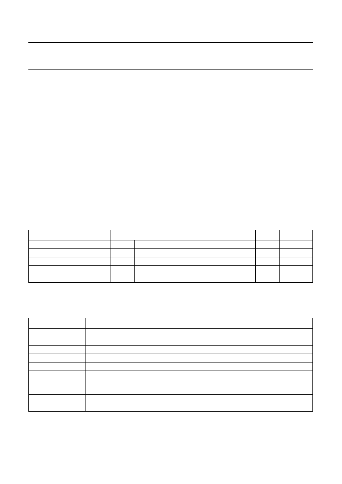
Table 1 I2C-bus data format
Note
1. Not available on 16-pin devices.
Table 2 Description of Table 1
BYTE MSB DATA BYTE LSB COMMAND
Address byte (ADB) 1 1 0 0 0 MA1 MA0 0 A
Divider byte 1 (DB1) 0 N14 N13 N12 N11 N10 N9 N8 A
Divider byte 2 (DB2) N7 N6 N5 N4 N3 N2 N1 N0 A
Control byte (CB) 1 CP T2 T1 T0 RSA RSB OS A
Ports byte (PB) P7
(1)
P6 P5
(1)
P4
(1)
XP2P1P0 A
SYMBOL DESCRIPTION
MA1, MA0 programmable address bits (see Table 3)
N14 to N0 programmable divider bits N = N14 × 2
14
+ N13 × 213+ ... + N1 × 2 + N0
CP charge-pump current; CP = 0 = 50 µA; CP = 1 = 250 µA
T2 to T0 test bits (see Table 4). For normal operation T2 = 0; T1 = 0; T0 = 1
RSA, RSB reference divider ratio select bits (see Table 5)
OS tuning amplifier control bit; for normal operation OS = 0 and tuning voltage is ON; when
OS = 1 tuning voltage is OFF (high impedance)
P2 to P0 PNP band switch buffers control bits
P7 to P4 NPN open collector control bits when P
n
= 0 output n is OFF; when Pn= 1 output n is ON
X don’t care
 Loading...