

Philips TEA1620P Technical data

查询TEA1620P供应商查询TEA1620P供应商
TEA1620P
STARplug
Rev. 01 — 17 March 2004 Product data sheet
1. General description
The TEA1620P is a Switched Mode Power Supply (SMPS) controller IC that operates
directly from the rectified universal mains. It is implemented in the high voltage EZ-HV™
SOI process, combined with a low voltage BICMOS process.
The device includes a high voltagepower switch and a circuit forstart-up directly from the
rectified mains voltage. A dedicated circuit for valley switching is built in, which makes a
very efficient slim-line electronic power-plug concept possible.
In its most basic version of application, the TEA1620P acts as a voltage source. Here, no
additional secondary electronicsarerequired. A combined voltageand current source can
be realized with minimum costs for external components. Implementation of the
TEA1620P renders an efficient and low cost power supply system.
2. Features
■ Designed for general purpose supplies
■ Integrated power switch: 48 Ω and 650 V
■ Operates from universal AC mains supplies: 80 V to 276 V
■ Adjustable frequency for flexible design
■ RC oscillator for load insensitive regulation loop constant
■ Valley switching for minimum switch-on loss
■ Frequency reduction at low power output for low standby power: <100 mW
■ Adjustable overcurrent protection
■ Undervoltage protection
■ Temperature protection
■ Short winding protection
■ Safe restart mode for system fault conditions
■ Simple application with both primary and secondary (opto) feedback
■ Available in 8-pin DIP package.
TM
3. Applications
■ Chargers
■ Adapters
■ TV and monitor standby supplies
■ PC peripherals.

Philips Semiconductors
4. Quick reference data
Table 1: Quick reference data
Symbol Parameter Conditions Min Typ Max Unit
V
CC(max)
V
DRAIN(max)
I
DRAIN
R
DSon
f
osc
T
amb
5. Ordering information
TEA1620P
STARplug
maximum supply voltage - - 40 V
maximum voltage at pin
DRAIN
supply current drawn from
pin DRAIN
drain-source on-state
resistance
oscillator frequency range 10 - 200 kHz
ambient temperature −20 - +85 °C
Tj>0°C - - 650 V
no auxiliary supply - 0.5 - mA
I
SOURCE
= −0.06 A
=25°C - 48 55.2 Ω
T
j
= 100 °C - 68 78.2 Ω
T
j
TM
Table 2: Ordering information
Type number Package
Name Description Version
TEA1620P DIP8 plastic dual in-line package; 8 leads (300 mil) SOT97-1
9397 750 12577 © Koninklijke Philips Electronics N.V. 2004. All rights reserved.
Product data sheet Rev. 01 — 17 March 2004 2 of 16
Philips Semiconductors
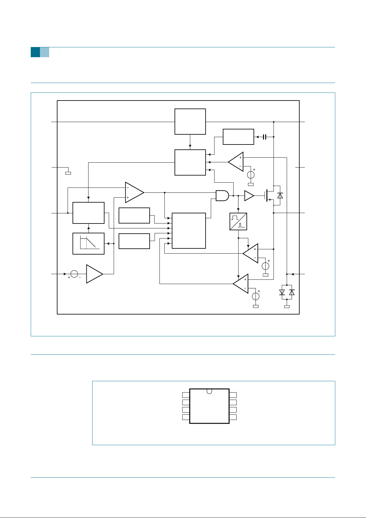
6. Block diagram
TEA1620P
STARplug
TM
V
CC
GND
RC
REG
1
2
stop
3
OSCILLATOR
low frequency
f
2.5 V
4
1.8 U
10x
TEA1620P
PWM
THERMAL
SHUTDOWN
POWER-UP
RESET
SUPPLY
LOGIC
PROTECTION
LOGIC
overcurrent
short winding
VALLEY
blank
100 mV
0.5 V
8
7
6
5
DRAIN
n.c.
SOURCE
AUX
0.75 V
col006
Fig 1. Block diagram.
7. Pinning information
7.1 Pinning
V
1
CC
GND n.c.
2
3
4
TEA1620P
001aaa308
RC SOURCE
REG AUX
Fig 2. Pin configuration.
9397 750 12577 © Koninklijke Philips Electronics N.V. 2004. All rights reserved.
Product data sheet Rev. 01 — 17 March 2004 3 of 16
8
7
6
5
DRAIN

Philips Semiconductors
7.2 Pin description
Table 3: Pin description
Symbol Pin Description
V
CC
GND 2 ground
RC 3 frequency setting
REG 4 regulation input
AUX 5 input for voltage from auxiliary winding for timing (demagnetization)
SOURCE 6 source of internal MOS switch
n.c. 7 not connected
DRAIN 8 drain of internal MOS switch; input for start-up current and valley sensing
1 supply voltage
8. Functional description
The TEA1620P is the heart of a compact flyback converter, with the IC placed at the
primary side. The auxiliary winding of the transformer can be used for indirect feedback to
control the isolated output. This additional winding also powers the IC. A more accurate
control of the output voltage and/or current can be implemented with an additional
secondary sensing circuit and optocoupler feedback.
TEA1620P
STARplug
TM
The TEA1620P uses voltage mode control. The frequency is determined by the maximum
transformer demagnetizing time and the time of the oscillator. In the first case, the
converter operates in the Self Oscillating PowerSupply (SOPS) mode. In the latter case, it
operates at a constant frequency, which can be adjusted with external components R
and CRC. This mode is called Pulse Width Modulation (PWM). Furthermore, a primary
stroke is started only in a valley of the secondary ringing. This valley switching principle
minimizes capacitive switch-on losses.
8.1 Start-up and undervoltage lock-out
Initially, the IC is self supplying from the rectified mains voltage. The IC starts switching as
soon as the voltage on pin VCCpasses the V
CC(start)
level. The supply is taken over by the
auxiliary winding of the transformer as soon as VCC is high enough and the supply from
the line is stopped for high efficiency operation.
As soon as the voltage on pin VCC drops below the V
CC(stop)
level, the IC stops switching
and restarts from the rectified mains voltage.
8.2 Oscillator
The frequency of the oscillator is set by the external resistor and capacitor on pin RC. The
external capacitor is charged rapidly to the V
stroke, it discharges to the V
level. Because the discharge is exponential, the
RC(min)
RC(max)
relative sensitivity of the duty factor to the regulation voltage at low duty factor is almost
equal to the sensitivity at high duty factors. This results in a more constant gain over the
duty factor range compared to PWM systems with a linear sawtooth oscillator. Stable
operation at low duty factors is easily realized. For high efficiency, the frequency is
reduced as soon as the duty factor drops below a certain value. This is accomplished by
increasing the oscillator charge time.
leveland, starting from a new primary
RC
9397 750 12577 © Koninklijke Philips Electronics N.V. 2004. All rights reserved.
Product data sheet Rev. 01 — 17 March 2004 4 of 16

Philips Semiconductors
To ensure that the capacitor can be charged within the charge time, the value of the
oscillator capacitor should be limited to approximately 1 nF.
8.3 Duty factor control
The duty factor is controlled by the internal regulation voltage and the oscillator signal on
pin RC. The internal regulation voltage is equal to the external regulation voltage (minus
2.5 V) multiplied by the gain of the error amplifier (typical 20 dB or 10 ×).
The minimum duty factor of the switched mode power supply is 0 %. The maximum duty
factor is set to 75 % (typical value at 100 kHz oscillation frequency).
8.4 Valley switching
A new cycle is started at the primary stroke when the switch is switched on (see Figure 3).
After a certain time (determined by the RC oscillator voltage and the internal regulation
level), the switch is turned off and the secondary stroke starts. The internal regulation
level is determined by the voltage on pin REG. After the secondary stroke, the drain
voltage shows an oscillation with a frequency of approximately
Where:
TEA1620P
STARplug
1
------------------------------
2π LpC
×
p
TM
Lp is the primary self inductance on the drain node
Cp is the parasitic capacitance on the drain node.
As soon as the oscillator voltage is high again and the secondary stroke has ended, the
circuit waits for a low drain voltage before starting a new primary stroke.
The primary stroke starts some time before the actual valley at low ringing frequencies,
and some time after the actual valley at high ringing frequencies. Figure 4 shows a typical
curve for a reflected voltage N × Vo of 80 V. This voltage is the output voltage Vo (see
Figure 5) transferred to the primary side of the transformer with the factor N (determined
by the turns ratio of the transformer). Figure 4 shows that the system switches exactly at
minimum drain voltage for ringing frequencies of 480 kHz, thus reducing the switch-on
losses to a minimum. At 200 kHz, the next primary stroke is started at 33° before the
valley. The switch-on losses are still reduced significantly.
9397 750 12577 © Koninklijke Philips Electronics N.V. 2004. All rights reserved.
Product data sheet Rev. 01 — 17 March 2004 5 of 16
 Loading...