


INTEGRATED CIRCUITS
DATA SH EET
TEA1620P
TM
STARplug
Preliminary specification
File under Integrated Circuits, IC11
2003 June 18

Philips Semiconductors Preliminary specification
STARplug
FEATURES
• Designed for general purpose supplies up to 50 W
• Integrated power switch:
– TEA1620: 48 Ω; 650 V
• Operates from universal AC mains supplies
(80 to 276 V)
• Adjustable frequency for flexible design
• RC oscillator for load insensitive regulation loop
constant
• Valley switching for minimum switch-on loss
• Frequency reduction at low power output makes low
standby power possible (<100 mW)
• Adjustable overcurrent protection
• Under voltage protection
• Temperature protection
• Short circuit winding protection
• Simple application with both primary and secondary
(opto) feedback
• Available in 8-pin DIP package.
TM
TEA1620P
Initsmostbasic version of application, the TEA1620P acts
as a voltage source. Here, no additional secondary
electronics are required. A combined voltage and current
source can be realized with minimum costs for external
components.ImplementationoftheTEA1620Prenders an
efficient and low cost power supply system.
APPLICATIONS
Typical application areas for the STARplugTM are:
• Chargers
• Adapters
• STB (Set Top Box)
• DVD
• CD(R)
• TV/monitor standby supplies
• PC peripherals
• PC Silverbox standby SMPS
• Microcontroller supplies in home applications and small
portable equipment, etc.
GENERAL DESCRIPTION
The TEA1620P is a Switched Mode Power
Supply (SMPS) controller IC that operates directly from
the rectified universal mains.Itis implemented in the high
voltage EZ-HV SOI process, combined with a low voltage
BICMOS process. The device includes a high voltage
power switch and a circuit for start-up directly from the
rectified mains voltage.
A dedicated circuit for valley switching is built in, which
makes a very efficient slim-line electronic powerplug
concept possible.
2003 June 18 2
Philips Semiconductors Preliminary specification
STARplug
TM
TEA1620P
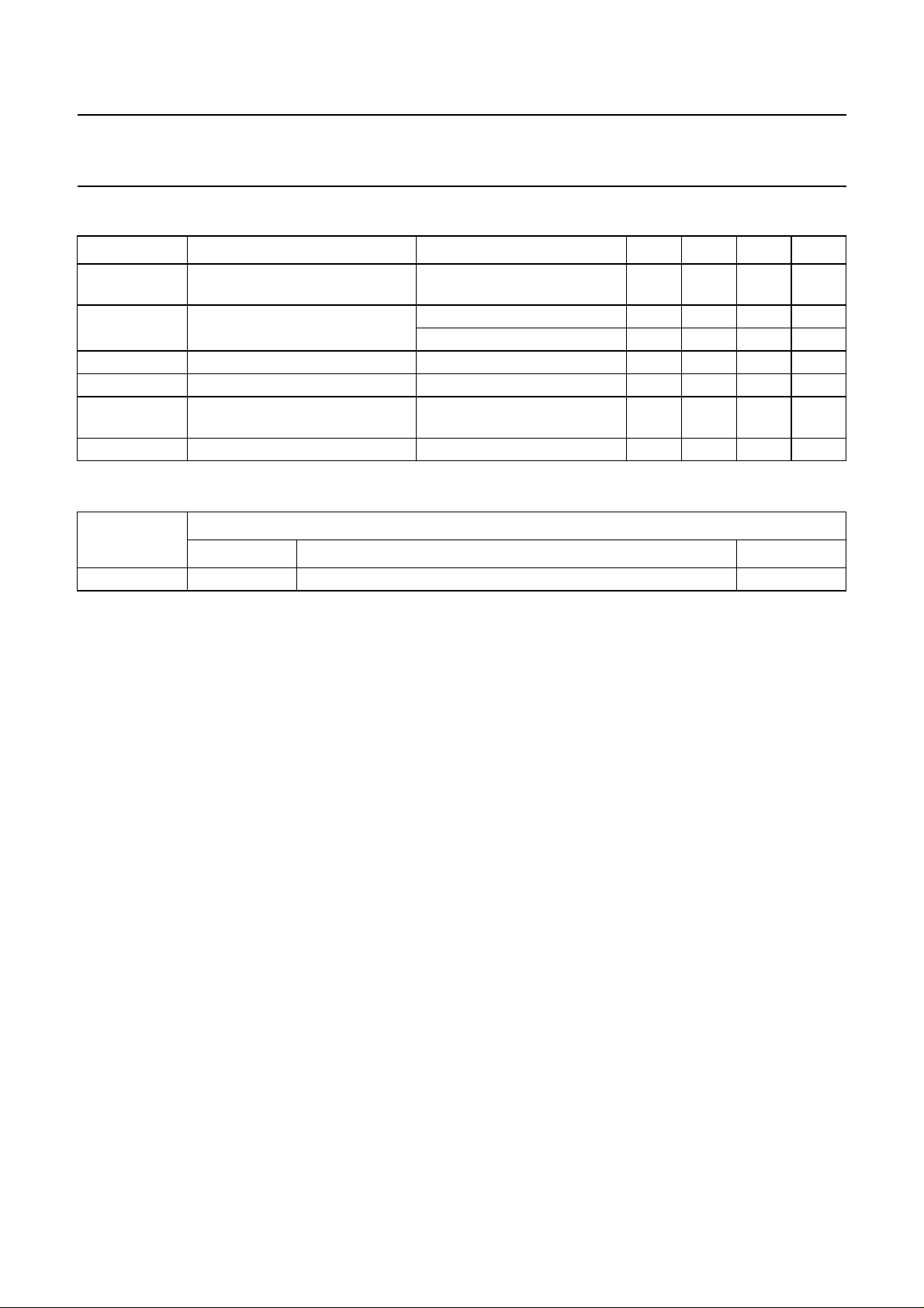
QUICK REFERENCE DATA
SYMBOL PARAMETER CONDITIONS MIN. TYP. MAX. UNIT
V
drain(max)
maximum voltage at the DRAIN
Tj>0°C −−650 V
pin
R
DS(on)
V
CC(max)
f
osc
I
drain
drain-source on-state resistance
of TEA1620
Tj=25°C; I
Tj= 100 °C; I
= −0.06 A − 48 55.2 Ω
source
= −0.06 A − 68 78.2 Ω
source
maximum supply voltage −−40 V
frequency range of oscillator 10 − 200 kHz
supply current drawn from DRAIN
no auxiliary supply − 0.5 − mA
pin
T
amb
ambient temperature −20 − +85 °C
ORDERING INFORMATION
TYPE
NUMBER
NAME DESCRIPTION VERSION
PACKAGE
TEA1620P DIP8 plastic dual in-line package; 8 leads (300 mil) SOT97-1
2003 June 18 3
Philips Semiconductors Preliminary specification
STARplug
BLOCK DIAGRAM
handbook, full pagewidth
CC
1
2
V
GND
TM
TEA152x
TEA1620P
SUPPLY
LOGIC
VALLEY
100 mV
TEA1620P
8
DRAIN
7
n.c.
RC
REG
3
4
stop
OSCILLATOR
low freq
F
1.8 U
2.5 V
10x
PWM
THERMAL
SHUTDOWN
POWER-UP
RESET
PROTECTION
LOGIC
overcurrent
short circuit winding
blank
0.5 V
0.75 V
MGT419
6
5
SOURCE
AUX
Fig.1 Block diagram.
2003 June 18 4

Philips Semiconductors Preliminary specification
STARplug
TM
PINNING
PIN
SYMBOL
DESCRIPTION
TEA1620P
V
CC
1 supply voltage
GND 2 ground
RC 3 frequency setting
REG 4 regulation input
AUX
5
input for voltage from auxiliary winding for timing
(demagnetization)
SOURCE 6 source of internal MOS switch
n.c. 7 not connected
DRAIN
8
drain of internal MOS switch; input for start-up current
and valley sensing
TEA1620P
handbook, halfpage
Fig.2 Pin configuration of TEA1620P.
V
CC
RC
REG
1
2
TEA152xP
TEA1620P
3
4
MGT420
DRAIN
8
n.c.GND
7
SOURCE
6
AUX
5
2003 June 18 5

Philips Semiconductors Preliminary specification
STARplug
TM
FUNCTIONAL DESCRIPTION
The TEA1620P is the heart of a compact flyback
converter, with the IC placed at the primary side. The
auxiliary winding of the transformer can be used for
indirect feedback to control the isolated output. This
additional winding also powers the IC. A more accurate
control of the output voltage and/or current can be
implemented with an additional secondary sensing circuit
and optocoupler feedback.
The TEA1620P uses voltage modecontrol. The frequency
isdeterminedbythemaximum transformer demagnetizing
time and the time of the oscillator. In the first case, the
converter operates in the Self Oscillating Power Supply
(SOPS) mode. In the latter case, it operates at a constant
frequency, which can be adjusted with external
components RRC and CRC. This mode is called Pulse
WidthModulation(PWM).Furthermore,aprimarystrokeis
startedonlyinavalleyofthesecondary ringing. This valley
switching principle minimizes capacitive switch-on losses.
Start-up and under voltage lock-out
Initially, the IC is self supplying from the rectified mains
voltage. The IC starts switching as soon as the voltage on
pin VCC passes the V
level. The supply is taken
CC(start)
over by the auxiliary winding of the transformer as soon as
VCCis high enough and the supply from the line is stopped
for high efficiency operation.
As soon as the voltage on pin VCC drops below the
V
CC(stop)
level, the IC stops switching and restarts from the
rectified mains voltage.
Oscillator
The frequency of the oscillator is set by the external
resistor and capacitor on pin RC. The external capacitor is
charged rapidly to the V
new primary stroke, it discharges to the V
level and, starting from a
RC(max)
RC(min)
level.
Because the discharge is exponential, the relative
sensitivity of the duty factor to the regulationvoltage at low
duty factor is almost equal to the sensitivity at high duty
factors. This results in a more constant gain over the duty
factor range compared to PWM systems with a linear
sawtooth oscillator. Stable operation at low duty factors is
easily realized. For high efficiency, the frequency is
reduced as soon as the duty factor drops below a certain
value. This is accomplished by increasing the oscillator
charge time.
TEA1620P
regulation voltage is equal to the external regulation
voltage (minus 2.5 V) multiplied by the gain of the error
amplifier (typical 20 dB (10 ×)).
Valley switching
A new cycle is started when the primary switch is switched
on (see Fig.3). After a certain time (determined by the
oscillator voltage RC and the internal regulation level), the
switch is turned off and the secondary stroke starts. The
internal regulation level is determined by the voltage on
pin REG. After the secondary stroke, the drain voltage
shows an oscillation with a frequency of approximately
---------------------------------------------------2 π× LpCp×()×()
where L
parasitic capacitance on the drain node.
As soon as the oscillator voltage is high again and the
secondary stroke has ended, the circuit waits for a low
drain voltage before starting a new primary stroke.
Figure 3 shows the drain voltage together with the valley
signal, the signal indicating the secondary stroke and the
RC voltage.
The primary stroke starts some time before the actual
valley at low ringing frequencies, and some time after the
actual valley at high ringing frequencies. Figure 4 shows a
typical curve for a reflected output voltage N × V
This voltage is the output voltage Vo (see Fig.5)
transferred to the primary side of the transformer with the
factor N (determined by the turns ratio of the transformer).
Figure 4 shows that the system switches exactly at
minimum drain voltage for ringing frequencies of 480 kHz,
thus reducing the switch-on losses to a minimum.
At 200 kHz,the next primary stroke is started at 33°before
the valley. The switch-on losses are still reduced
significantly.
Demagnetization
Thesystemoperatesindiscontinuousconductionmodeall
the time. As long as the secondary stroke has not ended,
the oscillator will not start a new primarystroke. During the
first t
suppressed. This suppression may be necessary in
applications where the transformer has a large leakage
inductance and at low output voltages.
1
is the primary self inductance and Cp is the
p
seconds, demagnetization recognition is
suppr
of 80 V.
o
Duty factor control
The duty factor is controlled by the internal regulation
voltage and the oscillator signal on pin RC. The internal
2003 June 18 6
 Loading...