


查询TEA1566供应商
INTEGRATED CIRCUITS
DATA SH EET
TEA1566
GreenChip; SMPS module
Preliminary specification
File under Integrated Circuits, IC11
1999 Apr 20
Philips Semiconductors Preliminary specification
GreenChip; SMPS module TEA1566
FEATURES
Distinctive features
• High level of integration results in 20 to 50 fewer
components compared to a power supply with discrete
components
• On-chip 600 V MOSFET
• On/off function replaces expensive mains switch with
functional switch
• Direct off-line operation (90 to 276 VAC)
• On-chip 5% accurate oscillator.
Green features
• Low power consumption in off-mode (<100 mW)
• On-chip efficient start-up current source giving fast
start-up
• Burst mode stand-by (<2 W) for overall improved
system efficiency
• Low power operation mode with lower frequency to
reduce switching losses.
Protection features
APPLICATIONS
mains
TEA1566
9
8
7
6
5
4
3
2
1
output
Vin
NC
OOB
Dem
Gnd
Vctrl
Iref
Vaux
Isense
• Demagnetization protection
• Cycle by cycle current limitation with programmable
current trip level
• Over voltage protection
• Over temperature protection
• Safe-restart mode with reduced power for system fault
conditions.
Highly versatile
• Usable in Buck and flyback topology
• Interfaces both primary and secondary side feedback.
MGR691
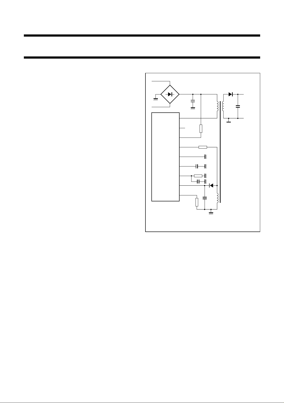
Fig.1 Typical flyback application.
GENERAL DESCRIPTION
The GreenChip, intended for off-line 90 to 276 VAC
power supply applications, is a monolithic high voltage
family of ICs that combines analog and digital circuits to
implement all necessary control functions for a switched
mode power supply. The functions include integrated high
voltage start-up current source, voltage mode PWM
control, 5% accurate trimmed oscillator, band gap derived
reference voltages, comprehensive fault protection, and
leading edge blanking. High level of integration leads to
cost effective power supplies that are compact, weigh less,
and at the same time give higher efficiency, are more
reliable and simple to design. Efficient green features lead
to very low power operation modes and a novel on/off
function helps replace the expensive mains switch with a
low cost functional switch.
1999 Apr 20 2
Philips Semiconductors Preliminary specification
GreenChip; SMPS module TEA1566
ORDERING INFORMATION
TYPE NUMBER
PACKAGE
NAME DESCRIPTION VERSION
TEA1566S SIL9P plastic single in-line power package; 9 leads SOT131-2
TEA1566J DBS9P plastic DIL-bent-SIL power package; 9 leads (lead length12 mm) SOT157-2
BLOCK DIAGRAM
handbook, full pagewidth
OOB
Vaux
VAUX
ON/OFF
1 kΩ
7
MANAGEMENT
CURRENT SOURCE
START-UP
TEA1566
VinIref
923
Vctrl
Dem
4
6
5.5 V
SAMPLE
AND
HOLD1
DEMAGNETIZATION
NEGATIVE
CLAMP
burst mode
stand-by
TEMPERATURE
MANAGEMENT
OVER
PROTECTION
SAMPLE
AND
HOLD2
amplifier
OSCILLATOR
Fig.2 Block diagram.
error
5
Gnd
PWM
comparator
R
Q
S
OVER CURRENT
PROTECTION
LEADING EDGE
BLANKING
FREQUENCY
CONTROL
81
NC
driver
stage
power
MOSFET
6 Ω
MGR692
Isense
1999 Apr 20 3
Philips Semiconductors Preliminary specification
GreenChip; SMPS module TEA1566
PINNING
SYMBOL PIN DESCRIPTION
Isense 1 programmable current sense
resistor
Vaux 2 IC supply capacitor
Iref 3 reference resistor for setting
internal reference currents
Vctrl 4 feedback voltage for duty cycle
control
Gnd 5 ground
Dem 6 demagnetization input signal from
primary side auxiliary winding
OOB 7 on/off/burst mode input signal
NC 8 not connected
Vin 9 MOSFET drain connection
handbook, halfpage
Isense
Vaux
Iref
Vctrl
Gnd
Dem
OOB
NC
Vin
1
2
3
4
5
6
7
8
9
TEA1566
MGR693
Fig.3 Pin configuration.
FUNCTIONAL DESCRIPTION
The GreenChip family of ICs are highly integrated, with
most common PWM functions like error amplifier,
oscillator, bias current generator, and band gap based
reference voltage circuits fully integrated in the ICs.
High level of integration leads to easy and cost effective
design of power supplies.The ICs have been fabricated in
a Philips proprietary high voltage BCDMOS process that
enables devices of up to 720 V to be fabricated on the
same chip with low voltage circuitry.
An efficient on-chip start-up circuit enables fast start-up
and dissipates negligible power after start up. On-chip
accurate oscillator generates a saw tooth waveform which
is used by the voltage mode feedback control circuitry to
generate a pulse width modulated signal for driving the
gate of the power MOSFET. A novel regulation scheme is
used to implement both primary and secondary side
regulation to minimize external component count.
Protection features like over voltage, over current, over
temperature, and demagnetization protection, give
comprehensive safety against system fault conditions.
The GreenChip offers some advanced features that
greatly enhance the efficiency of the overall system.
Off-mode reduces the power consumption of the IC below
100 mW. Burst mode stand-by reduces the power
consumption of the system to below 2 W. Low power
operation mode reduces the operating frequency of the
system, when the system is working under low load
conditions, to reduce the switching losses.
Start-up current source and Vaux management
A versatile on-chip start-up current source makes an
external, highly dissipating, trickle-charge circuit
unnecessary. See Fig.2 for the block diagram of the IC.
The start-up current source derives power from the mains
via pin Vin (drain). It supplies current (see symbols
‘Istart-low’ and ‘Istart-high’ of Chapter “Characteristics”) to
charge the Vaux (IC supply) capacitor and at the same
time provides current to the control circuitry of the IC. Once
the Vaux capacitor is charged to its start-up voltage level
(11 V), the on-chip oscillator starts oscillating and the IC
starts switching the power MOSFET. Power is then
supplied to the load capacitor via the secondary winding.
Figure 1 shows a typical flyback application diagram.
The Vaux capacitor is also supplied by an auxiliary
winding on the primary side. This winding is coupled to the
secondary side winding supplying the output capacitor.
As the output capacitor voltage increases and approaches
its nominal value, the re-supply of the Vaux capacitor is
done by the auxiliary winding. Figure 4 shows relevant
waveforms at start-up. For successful take over of supply
of Vaux capacitor by the auxiliary winding, it is important
that the re-supply of Vaux capacitor starts before its
voltage drops to its Under Voltage Lockout (UVLO) level of
8.05 V of the system and stops delivering power to the
output.
1999 Apr 20 4
Philips Semiconductors Preliminary specification
GreenChip; SMPS module TEA1566
In case of output short circuit, the Vaux capacitor is no
longer supplied by the auxiliary winding and its voltage
drops till it reaches the UVLO level. If the output is an open
circuit, the output voltage will rise till it reaches the Over
Voltage Protection (OVP) level. The IC will detect this state
and stop switching.
In absence of switching of the power device, the Vaux
capacitor will not be re-supplied and its voltage will drop till
it reaches UVLO level. Once the Vaux voltage drops to
UVLO level, the start-up current source is re-activated and
it charges the Vaux capacitor to its start level and the
system goes through a cycle similar to the start-up cycle.
Figure 5 shows the relevant waveforms during safe-restart
mode. The charging current (see symbol ‘Irestart-prot’ in
Chapter “Characteristics”) from the start-up circuit during
the safe-restart mode is lower than the normal start-up
current (see symbol ‘Istart-high’ in
Chapter “Characteristics”) in order to implement a low
“hiccup” duty cycle. This helps insure devices on the
output secondary winding do not get destroyed during
output short circuit, violating safety conditions.
The start-up current source also plays a key role in
implementation of burst mode stand-by (see symbol
‘Irestart-stby’ in Chapter “Characteristics”), which will be
explained later.
Vaux
Vout
Vgate
(1) Start-up current charges capacitor V
(2) Charging of capacitor V
11 V
(2)
8.05 V
(1)
switchingoff
.
is taken-over by the auxiliary winding.
aux
aux
Fig.4 Normal start-up waveforms.
t
t
t
MGR694
handbook, full pagewidth
(1) Start-up current source charges capacitor V
Vaux
Vgate
normal operation
.
aux
fault condition
(1)
switching off
Fig.5 Safe-start mode waveforms.
1999 Apr 20 5
MGR695
t
t
Philips Semiconductors Preliminary specification
GreenChip; SMPS module TEA1566
Reference
All reference voltages are derived from a temperature
compensated, on-chip, band gap. The band gap reference
voltage is also used, together with an external resistor
connected at pin Iref, to generate accurate, temperature
independent, bias currents in the chip:
V
REF
I
REF
=
------------- R
REF
[A]
The frequency of the controller is also set by the reference
resistor Rref (also see Section “Oscillator”).
Sample and hold
GreenChip ICs employ voltage mode feedback for
regulating the output voltage. In primary feedback mode, a
novel sample and hold circuit is used. The sample and
hold circuit works by sampling the current into pin Dem,
which is related to the output voltage via Rdem, during the
time that the secondary current is flowing:
a × V
V
dem+
out=Iref
× R
dem+Vdem+
where:
is specified in chapter “Characteristics”
a = a constant determined by turn ratio of the
transformer.
This sampled current information is stored on the external
capacitor connected to pin Vctrl. The pulse width
modulator uses this voltage information to set the duty
cycle of operation for the power MOSFET. In secondary
feedback, the feedback voltage is provided by an
opto-coupler.
Oscillator
The oscillator is used to set the switching duty cycle by
comparing the oscillator ramp to the output of the error
amplifier in the pulse width modulator circuit.The oscillator
is fully integrated and works by charging and discharging
an internal capacitor between two voltage levels to create
a sawtooth waveform with a rising edge which is 80% of
the oscillator cycle. This ratio is used to set a maximum
switching duty cycle of 80% for the IC. The oscillator is
internally trimmed to 5% accuracy. The oscillator
frequency can be adjusted between 50 to 100 kHz
(see symbol f
osc-h-range
in Chapter “Characteristics”) by
changing the external reference resistor (see symbol Rref
in Chapter “Characteristics”) that sets the chip bias
currents. This gives additional flexibility to the power
supply designer in the choice of his system
components.The frequency is correlated with the value of
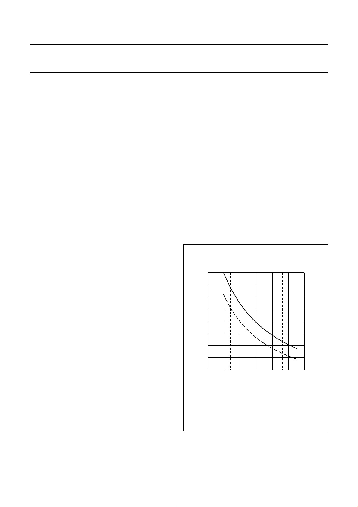
the reference resistor Rref (see Fig.6).
In Chapter “Characteristics” f
osc-typical
osc-l
and f
osc-h
and
, f
the Rref operating resistor range are specified.
MGR936
110
handbook, halfpage
high
frequency
(kHz)
90
55
low
frequency
(kHz)
45
Pulse width modulator
The pulse width modulator, which is made up of an
inverting error amplifier and a comparator (see Fig.2),
drives the power MOSFET with a duty cycle which is
inversely proportional to the voltage on pin Vctrl.
In primary feedback mode, this is the voltage on the
sample and hold capacitor and in secondary feedback
mode, this voltage is provided by an opto-coupler. A signal
from the oscillator sets a latch that turns on the power
MOSFET. The latch is reset by the signal from the pulse
width modulator or by the duty cycle limiting circuit.
The latching PWM mode of operation prevents multiple
switching of the power switch. The maximum duty cycle is
set internally at 80%.
Figure 7 shows the normal switching operation of the IC.
1999 Apr 20 6
70
50
30
10 20 30 40
(1) High frequency mode.
(2) Low frequency mode.
(1)
(2)
Fig.6 Frequency as function of the R
R
REF
(kΩ)
REF
35
25
15
value.

Philips Semiconductors Preliminary specification
GreenChip; SMPS module TEA1566
Multi frequency control
The oscillator is also capable of working at a lower
frequency (see f
in Chapter “Characteristics”). A ratio
osc-l
of 1 : 2.5 is maintained between high and low frequency of
the oscillator. Low frequency operation is invoked if the
power supply is working at or below one ninth of its peak
power. By working at a lower frequency, the switching
losses in the power supply are reduced. A novel scheme
is used to ensure that the transfer of high to low frequency
and vice versa has no effect on the regulation of the output
voltage.
Gate driver
The gate driver has a totem-pole output stage that has
current sourcing capability of 120 mA and a current sink
capability of 550 mA. This is to enable fast turn on and turn
off of the power device for efficient operation.
A lower driver source current has been chosen in order to
limit the ∆V/∆t at switch-on. This is advantageous for EMI
(ElectroMagnetic Interference) and reduces the current
spike across Rsense.
Demagnetization protection
This feature guarantees discontinuous conduction mode
operation for the power supply which simplifies the design
of feedback control and gives faster transient response.
Demagnetization protection is an additional protection
feature that protects against saturation of the
transformer/inductor. Demagnetization protection also
protects the power supply components against excessive
stresses at start-up, when all energy storage components
are completely discharged. The converter is cycle by cycle
protected during shorted output system fault condition due
to the demagnetization protection. The value of the
demagnetization resistor (R
) can be calculated with the
dem
formula given in Section “Sample and hold”.
Negative clamp
The negative clamp circuit does not let the voltage on
pin Dem go below −0.4 V, when the auxiliary winding
voltage goes negative during the time that the power
device is turned on, to ensure correct operation of the IC.
Over voltage protection
An Over Voltage Protection (OVP) mode has been
implemented in the GreenChip series. This circuit works
by sensing the Vaux voltage. If the output voltage exceeds
the preset voltage limit, the OVP circuit turns off the power
MOSFET. With no switching of the power device, the Vaux
capacitor is not re-supplied and discharges to UVLO level
and the system goes into the low dissipation safe-restart
mode described earlier. The system recovers from the
safe-restart mode only if the OVP condition is removed.
Over current protection
Cycle by cycle Over Current Protection (OCP) is provided
by sensing the voltage on an external resistor which is
connected to the source of the power MOSFET.
The voltage on the current sense resistor, which reflects
the amplitude of the primary current, is compared
internally with a reference voltage using a high speed
comparator. This threshold voltage is specified as V
th(Imax)
in the chapter “Characteristics”. The maximum primary
V
(protection) current is therefore: [A]
I
prot
th Imax()
=
-----------------------R
sense
If the power device current exceeds the current limit, the
comparator trips and turns off the power device.
The power device is typically turned off in 210 ns
(see tDin Chapter “Characteristics”).
The availability of the current sense resistor off-chip for
programming the OCP trip level increases design flexibility
for the power supply designer. An off-chip current sense
resistor also reduces the risk of an OCP condition being
sensed incorrectly. At power MOSFET turn-on the
∆V/∆t limiters capacitance discharge current does not
have to flow through the sense resistor, because this
capacitor can be connected between drain and source of
the power MOSFET directly.
The Leading Edge Blanking (LEB) circuit works together
with the OCP circuit and inhibits the operation of the OCP
comparator for a short duration (see t
LEB
in
Chapter “Characteristics”) when the power device is
turned on. This ensures that the power device is not turned
off prematurely due to false sensing of an OCP condition
because of current spikes caused by discharge of
primary-side snubber and parasitic capacitances.
LEB time is not fixed and it tracks the oscillator frequency.
1999 Apr 20 7

Philips Semiconductors Preliminary specification
GreenChip; SMPS module TEA1566
Over temperature protection
Protection against excessive temperature is provided by
an analog temperature sensing circuit that turns off the
power device when the temperature exceeds typically
140 °C.
On/off mode
The expensive mains switch can be replaced by an
in-expensive functional switch by using the on/off mode.
Figure 13 shows a flyback converter configured to use the
on/off mode. Depending upon the position of switch S1,
either voltage close to ground or a voltage of greater than
typical 2.5 V exists on pin OOB.
The difference between these voltages is detected
internally by the IC. The IC goes into the off-mode if the
voltage is low, where it consumes a current of typical
350 µA (see Iin-off in Chapter “Characteristics”). If the
voltage on pin OOB is typically 2.5 V (see Von/off in
Chapter “Characteristics”), the IC goes through the
start-up sequence and commences normal operation.
In Fig.14 a Mains Under Voltage Lock Out (MUVLO)
function has been created using 3 resistors. Assuming that
R3 is chosen very high ohmic, the GreenChip™ starts
operating if:
V
MAINS
R1
------- R2
V
OOB
R1 R2»()×≈
Burst mode stand-by
Pin OOB is also used to implement the burst mode
stand-by. In burst mode stand-by, the power supply goes
into a special low dissipation state where it typically
consumes less than 2 W of power. Figure 14 shows a
flyback converter using the burst mode stand-by feature.
The system enters burst mode when the microcontroller
closes switches S2 and S3 on the secondary side.
Switch S2 shorts the output capacitor to the voltage level
of the microcontroller capacitor. The output secondary
winding now supplies the microcontroller capacitor. When
the voltage on the microcontroller capacitor exceeds the
zener voltage (V
) the opto-coupler is activated which
z
sends a signal to pin OOB. In response to this signal, the
IC stops switching and goes into a “hiccup” mode.
Figure 7 shows the burst-mode operation graphically.
The hiccup mode during burst mode operation differs from
the hiccup in safe-restart mode during system fault. For
safe restart mode, the power has to be reduced. For burst
mode, sufficient power to supply the microcontroller has to
be delivered. To prevent transformer rattle, the
transformer peak current is reduced by a factor of 3.
Burst mode stand-by operation continues till the
microcontroller opens switches S2 and S3. The system
then goes through the start-up sequence and commences
normal switching behaviour.
In this way it is assured that the power supply only starts
working above a Vmains of e.g. 80 V. The bleeder current
through R1 should be low (e.g. 30 µA at 300 V).
1999 Apr 20 8
 Loading...