

Philips TEA1533P, TEA1533AP DATA SHEET

INTEGRATED CIRCUITS
DATA SH EET
TEA1533P; TEA1533AP
GreenChip
Product specification
Supersedes data of 2002 May 31
TM
II SMPS control IC
2002 Aug 23

Philips Semiconductors Product specification
GreenChipTMII SMPS control IC
FEATURES
Distinctive features
• Universal mains supply operation (70 to 276 V AC)
• High level of integration, giving a very low external
component count.
Green features
• Valley or zero voltage switching for minimum switching
losses
• Efficient quasi-resonant operation at high power levels
• Frequency reductionat low power standby for improved
system efficiency (<3 W)
• Cycle skipping mode at very low loads. Pi <300 mW at
no-load operation for a typical adapter application
• On-chip start-up current source.
Protection features
• Safe restart mode for system fault conditions
• Continuous mode protection by means of
demagnetization detection (zero switch-on current)
• Accurateand adjustable overvoltage protection(latched
in TEA1533P, safe restart in TEA1533AP)
• Short winding protection
• Undervoltage protection (foldback during overload)
• Overtemperatureprotection (latched in TEA1533P,safe
restart in TEA1533AP)
• Low and adjustable overcurrent protection trip level
• Soft (re)start
• Mains voltage-dependent operation enabling level.
TEA1533P; TEA1533AP
APPLICATIONS
Besides typical application areas, i.e. adapters and
chargers, the device can be used in TV and monitor
supplies and all applications that demand an efficient and
cost-effective solution up to 250 W.
1
2
TEA1533P
TEA1533AP
3
4
8
7
6
5
MGU505
2002 Aug 23 2
Fig.1 Basic application diagram.

Philips Semiconductors Product specification
GreenChipTMII SMPS control IC
GENERAL DESCRIPTION
The GreenChip
Switched Mode Power Supply (SMPS) control ICs
operatingdirectly from the rectified universalmains.A high
level of integration leads to a cost effective power supply
with a very low number of external components.
The special built-in green functions allow the efficiency to
be optimum at all power levels. This holds for
quasi-resonant operation at high power levels, as well as
fixed frequency operation with valley switching at medium
power levels. At low power (standby) levels, the system
operates at a reduced frequency and with valley detection.
(1) GreenChip is a trademark of Koninklijke Philips
Electronics N.V.
ORDERING INFORMATION
TYPE NUMBER
TEA1533P DIP8 plastic dual in-line package; 8 leads (300 mil) SOT97-1
TEA1533AP
(1)
II is the second generation of green
NAME DESCRIPTION VERSION
The proprietary high voltage BCD800 process makes
direct start-up possible from the rectified mains voltage in
an effective and green way. A second low voltage
BICMOS IC is used for accurate, high-speed protection
functions and control.
Highly efficient and reliable supplies can easily be
designed using the GreenChipII control IC.
PACKAGE
TEA1533P; TEA1533AP
2002 Aug 23 3
This text is here in white to force landscape pages to be rotated correctly when browsing through the pdf in the Acrobat reader.This text is here in
b
_white to force landscape pages to be rotated correctly when browsing through the pdf in the Acrobat reader.This text is here inThis text is here in
white to force landscape pages to be rotated correctly when browsing through the pdf in the Acrobat reader. white to force landscape pages to be ...
2002 Aug 23 4
ook, full pagewidth
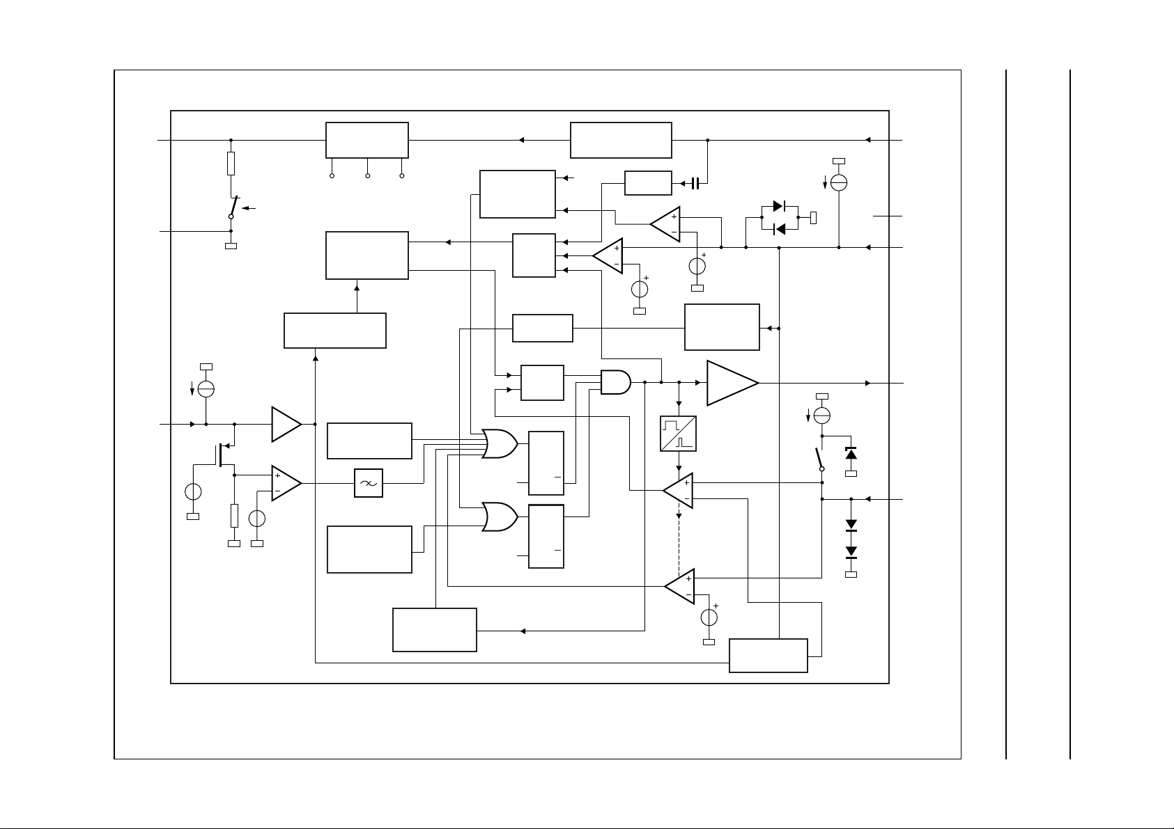
BLOCK DIAGRAM
Philips Semiconductors Product specification
GreenChip
V
CC
GND
CTRL
1
I
prot(CTRL)
M-level
−1
burst
detect
S1
2
3
2.5 V
SUPPLY
MANAGEMENT
internal
FREQUENCY
UVLO start
supply
VOLTAGE
CONTROLLED
OSCILLATOR
CONTROL
POWER-ON
RESET
OVER-
TEMPERATURE
PROTECTION
DEMAG
SHORT
PROTECTION
UVLO
V
< 4.5 V
CC
or UVLO
(TEA1533AP)
LOGIC
UP/DOWN
COUNTER
LOGIC
SQ
R
Q
SQ
R
Q
START-UP
CURRENT SOURCE
OCP
VALLEY
100
mV
50
mV
VOLTAGE
PROTECTION
LEB
blank
OCP
OVER-
DRIVER
I
prot(DEM)
clamp
soft
start
S2
8
DRAIN
TM
HVS
7
n.c.
4
DEM
6
DRIVER
I
ss
0.5 V
5
I
sense
II SMPS control IC
TEA1533P; TEA1533AP
TEA1533P
TEA1533AP
MAXIMUM
ON-TIME
PROTECTION
Fig.2 Block diagram.
short
winding
0.88 V
OVERPOWER
PROTECTION
MGU506
Philips Semiconductors Product specification
GreenChipTMII SMPS control IC
TEA1533P; TEA1533AP
PINNING FUNCTIONAL DESCRIPTION
SYMBOL PIN DESCRIPTION
V
CC
1 supply voltage
GND 2 ground
CTRL 3 control input
The TEA1533 is the controller of a compact flyback
converter, and is situated at the primary side. An auxiliary
winding of the transformer provides demagnetization
detection and powers the IC after start-up.
The TEA1533 can operate in multi modes (see Fig.4).
DEM 4 input from auxiliary winding for
demagnetization timing, overvoltage
and overpower protection
I
sense
DRIVER 6 gate driver output
HVS 7 high voltage safety spacer, not
5 programmable current sense input
handbook, halfpage
(kHz)
f
VCO fixed quasi resonant
175
connected
DRAIN 8 drain of external MOS switch, input for
start-up current and valley sensing
25
MGU508
P (W)
handbook, halfpage
V
1
CC
GND
2
TEA1533P
CTRL
DEM
TEA1533AP
3
4
MGU507
Fig.3 Pin configuration.
8
7
6
5
DRAIN
HVS
DRIVER
I
sense
Fig.4 Multi modes operation.
The next converter stroke is started only after
demagnetization of the transformer current (zero current
switching), while the drain voltage has reached the lowest
voltage to prevent switching losses (green function). The
primary resonant circuit of the primary inductance and
draincapacitorensuresthis quasi-resonant operation. The
design can be optimized in such a way that zero voltage
switching can be reached over almost the universal mains
range.
To prevent very high frequency operation at lower loads,
the quasi-resonant operation changes smoothly in fixed
frequency PWM control.
At very low power (standby) levels, the frequency is
controlled down, via the VCO, to a minimum frequency of
approximately 25 kHz.
Start-up, mains enabling operation level and
undervoltage lock-out
Initially, the IC is self supplying from the rectified mains
voltage via pin DRAIN (see Figs 11 and 12). Supply
capacitor C
is charged by the internal start-up current
VCC
source to approximately 4 V or higher, depending on the
voltage on pin DRAIN.
2002 Aug 23 5

Philips Semiconductors Product specification
GreenChipTMII SMPS control IC
Once the drain voltage exceeds the M-level
(mains-dependent operation-enabling level), the start-up
current source will continue charging capacitor C
(switch S1 will be opened); see Fig.2. The IC will activate
the converter as soon as the voltage on pin VCC passes
the V
CC(start)
level.
The IC supply is taken over by the auxiliary winding as
soon as the output voltage reaches its intended level and
the IC supply from the mains voltage is subsequently
stopped for high efficiency operation (green function).
The moment the voltage on pin VCC drops below the
undervoltage lock-out level, the IC stops switching and
enters a safe restart from the rectified mains voltage.
Inhibiting the auxiliary supply by external means causes
the converter to operate in a stable, well defined burst
mode.
Supply management
All (internal) reference voltages are derived from a
temperature compensated, on-chip band gap circuit.
VCC
V
handbook, halfpage
sense(max)
Fig.5 V
handbook, halfpage
(kHz)
TEA1533P; TEA1533AP
0.52 V
sense(max)
f
175
1 V
(typ)
voltage as function of V
1.5 V
(typ)
175 kHz
V
MGU509
MGU233
CTRL
CTRL
.
Current mode control
Current mode control is used for its good line regulation
behaviour.
The ‘on-time’ iscontrolled by theinternally inverted control
voltage, which is compared with the primary current
information. The primary current is sensed across an
external resistor. The driver output is latched in the logic,
preventing multiple switch-on.
The internal control voltage is inverselyproportional to the
external control pin voltage, with an offset of 1.5 V. This
means that a voltage range from 1 to 1.5 V on pin CTRL
will result in an internal control voltage range from
0.5 to 0 V (a high external control voltage results in a low
duty cycle).
Oscillator
The maximum fixed frequency of the oscillator isset by an
internal current source and capacitor. The maximum
frequency is reduced once the control voltage enters the
VCO control window. Then, the maximum frequency
changeslinearly with thecontrol voltage untilthe minimum
frequency is reached (see Figs 5 and 6).
25
V
VCO
VCO
2
level
Fig.6 VCO frequency as function of V
level
sense(max) (V)
1
sense(max)
Cycle skipping
At very low power levels, a cycle skipping mode will be
activated. A high control voltage will reduce the switching
frequency to a minimum of 25 kHz. If the voltage on the
control pin is raised even more, switch-on of the external
power MOSFET will be inhibited until the voltage on the
control pin has dropped to a lower value again (see Fig.7).
For system accuracy, it is not the absolute voltage on the
control pin that will trigger the cycle skipping mode, but a
signal derived from the internal VCO will be used.
Remark 1:If the no-loadrequirementof the systemissuch
that the output voltage can be regulated to its intended
level at a switching frequency of 25 kHz or above, the
cycle skipping mode will not be activated.
Remark 2: As switching will stop when the voltage on the
control pin is raised above a certain level, the burst mode
has to beactivated by amicrocontroller or any other circuit
sending a 30 µs, 16 mA pulse to the control input
(pin CTRL) of the IC.
2002 Aug 23 6
Philips Semiconductors Product specification
GreenChipTMII SMPS control IC
handbook, full pagewidth
CTRL
1.5 V − V
CTRL
X2
V
x
150 mV
current
comparator
V
I
DRIVER
OSCILLATOR
DRIVER
I
sense
TEA1533P; TEA1533AP
f
osc
f
max
f
min
cycle
skipping
1
0
dV
2
dV
1
150
Vx (mV)
MGU510
Vx (mV)
The voltage levels dV1 and dV2 are fixed in the IC to 50 mV (typical) and 18 mV (typical) respectively.
Fig.7 The cycle skipping circuitry.
Demagnetization
The system will be in discontinuous conduction mode all
the time. The oscillator will not start a new primary stroke
until the secondary stroke has ended.
Demagnetization features a cycle-by-cycle output
short-circuit protection by immediately lowering the
frequency (longer off-time), thereby reducing the power
Minimum and maximum ‘on-time’
The minimum ‘on-time’ of the SMPS is determined by the
Leading Edge Blanking (LEB) time. The IC limits the
‘on-time’ to 50 µs. When the system desires an ‘on-time’
longer than 50 µs, a fault condition is assumed (e.g.
removed Ciin Fig.11), the IC will stop switching and enter
the safe restart mode.
level.
Demagnetizationrecognition is suppressedduringthe first
t
time. This suppression may be necessary in
suppr
applications where the transformer has a large leakage
inductance, at low output voltages and at start-up.
If pin DEM is open-circuit or not connected, a fault
condition is assumed and the converter will stop operating
immediately. Operation will recommence as soon as the
fault condition is removed.
If pin DEM is shorted to ground, again a fault condition is
assumed and the converter will stop operating after the
first stroke. The converter will subsequently enter the safe
restart mode. This situation will persist until the
short-circuit is removed.
2002 Aug 23 7

Philips Semiconductors Product specification
GreenChipTMII SMPS control IC
OverVoltage Protection (OVP)
An OVP mode is implemented in the GreenChip series.
This works for the TEA1533 by sensing the auxiliary
voltage via the current flowing into pin DEM during the
secondary stroke. The auxiliary winding voltage is a
well-defined replica of the output voltage. Any voltage
spikes are averaged by an internal filter.
Ifthe output voltage exceedstheOVP trip level, aninternal
counter starts counting subsequent OVP events. The
counter has been added to prevent incorrect OVP
detections which might occur during ESD or lightning
events. If the output voltage exceeds the OVP trip level a
fewtimes and notagain in asubsequent cycle, theinternal
counter will count down with twice the speed compared
with counting-up. However, when typical 10 cycles of
subsequent OVP events are detected, the IC assumes a
true OVP and the OVP circuit switches the power
MOSFET off. Next, the controller waits until the UVLO
level is reached on pin VCC. When VCC drops to UVLO,
capacitor C
Regarding the TEA1533P, this IC will not start switching
again. Subsequently, VCC will drop again to the UVLO
level, etc. Operation only recommences when the V
voltage drops below a level of approximately 4.5 V
(practically when V
period).
will be recharged to the V
VCC
has been disconnectedfor a short
mains
start
level.
CC
TEA1533P; TEA1533AP
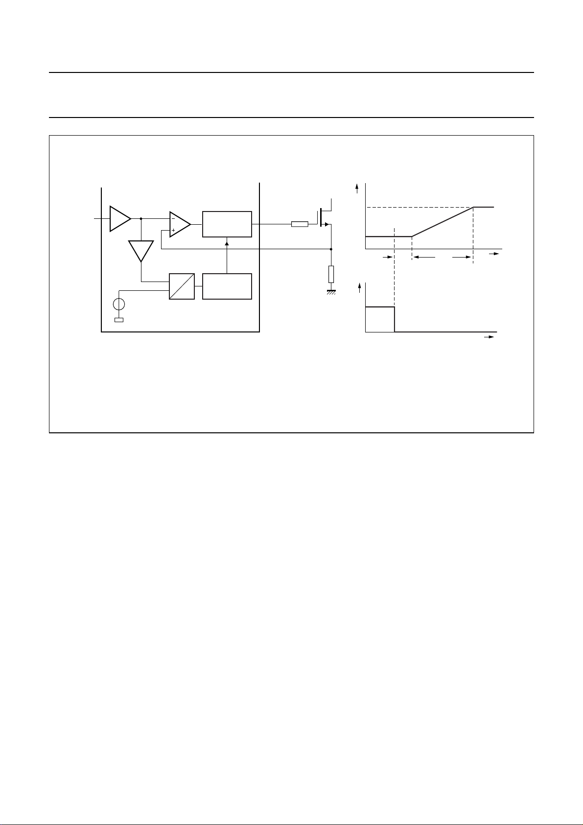
Valley switching
A new cycle starts when the power MOSFET is switched
on (see Fig.8). After the ‘on-time’ (which is determined by
the ‘sense’ voltage and the internal control voltage), the
switchis opened andthesecondary stroke starts.Afterthe
secondary stroke, the drain voltage shows an oscillation
with a frequency of approximately
----------------------------------------------2π×L
where L
is the primary self inductance of the transformer
p
and Cd is the capacitance on the drain node.
As soon as the oscillator voltage is high again and the
secondary stroke has ended, the circuit waits for the
lowest drain voltage before starting a new primary stroke.
This method is called valley detection. Figure 8 shows the
drain voltage together with the valley signal, the signal
indicating the secondary stroke and the oscillator signal.
In an optimum design, the reflected secondary voltage on
the primary side will force the drain voltage to zero. Thus,
zero voltage switching is very possible, preventing large
1
capacitive switching losses and
P
-- -
2
allowing high frequency operation, which results in small
and cost effective inductors.
1
C
×()×
p
d
2
CV
× f××=
Regarding the TEA1533AP, switching starts again (safe
restart mode) when the V
level is reached. This
start
process is repeated as long as the OVP condition exists.
Theoutput voltage V
can be set by the demagnetization resistor, R
V
N
----------N
=
o OVP()
s
I
(OVP)(DEM)RDEM
aux
× V
where Nsis the number of secondary turnsand N
atwhich the OVPfunctiontrips,
o(OVP)
:
DEM
+{}
clamp(DEM)(pos)
is the
aux
number of auxiliary turns of the transformer.
Current I
(OVP)(DEM)
The value of R
is internally trimmed.
can be adjusted to the turns ratio of the
DEM
transformer, thus making an accurate OVP possible.
2002 Aug 23 8
 Loading...