


查询TEA1532供应商查询TEA1532供应商
TEA1532
GreenChipII SMPS control IC
Rev. 01 — 28 May 2004 Preliminary data sheet
1. General description
The GreenChip™II is the second generation of green Switched Mode Power Supply
(SMPS) controller ICs. Its high level of integration allows the design of a cost effective
power supply with a very low number of external components.
The TEA1532 can also be used in fixed frequency, Continuous Conduction Mode (CCM)
converter designs for low voltage, high current applications. At low power (standby)levels,
the system operates in cycle skipping mode which minimizes the switching losses during
standby.
The special built-in green functions allow the efficiency to be optimum at all power levels.
This holds for quasi-resonant operation at high power levels, as well as fixed frequency
operation with valley switching at medium power levels. At low power (standby) levels,the
system operates in cycle skipping mode with valley detection.
2. Features
2.1 Distinctive features
2.2 Green features
2.3 Protection features
The proprietary high voltage BCD800 process makes direct start-up possible from the
rectified universal mains voltage in an effective and green way. A second low voltage
BICMOS IC is used for accurate, high speed protection functions and control.
The TEA1532 enables highly efficient and reliable supplies to be designed easily.
■ Universal mains supply operation (70 V to 276 VAC)
■ High level of integration, resulting in a very low external component count
■ Fixed frequency Continuous Conduction Mode (CCM) operation capability
■ Quasi-Resonant (QR) Discontinuous Conduction Mode (DCM) operation capability.
■ Valley or zero voltage switching for minimum switching losses in QR operation
■ Cycle skipping mode at very low loads; input power <300 mW at no-load operation for
a typical adapter application
■ On-chip start-up current source.
■ Safe restart mode for system fault conditions
■ Zero current switch-on in QR mode
■ Undervoltage protection (foldback during overload)

Philips Semiconductors
■ IC overtemperature protection (latched)
■ Low and adjustable overcurrent protection trip level
■ Soft (re)start
■ Mains voltage-dependent operation-enabling level
■ General purpose input for latched or safe restart protection and timing, e.g. to be used
for overvoltage protection (OVP), output short-circuit protection or system
overtemperature protection
■ Brown-out protection.
3. Applications
■ Printer adapters and chargers. The device can also be used in all applications that
demand an efficient and cost-effective solution up to 250 W.
4. Ordering information
Table 1: Ordering information
Type number Package
TEA1532T SO8 plastic small outline package; 8 leads; body
TEA1532P DIP8 plastic dual in-line package; 8 leads (300 mil) SOT97-1
TEA1532
GreenChipII SMPS control IC
Name Description Version
SOT96-1
width 3.9 mm
9397 750 13113 © Koninklijke Philips Electronics N.V. 2004. All rights reserved.
Preliminary data sheet Rev. 01 — 28 May 2004 2 of 27
Philips Semiconductors
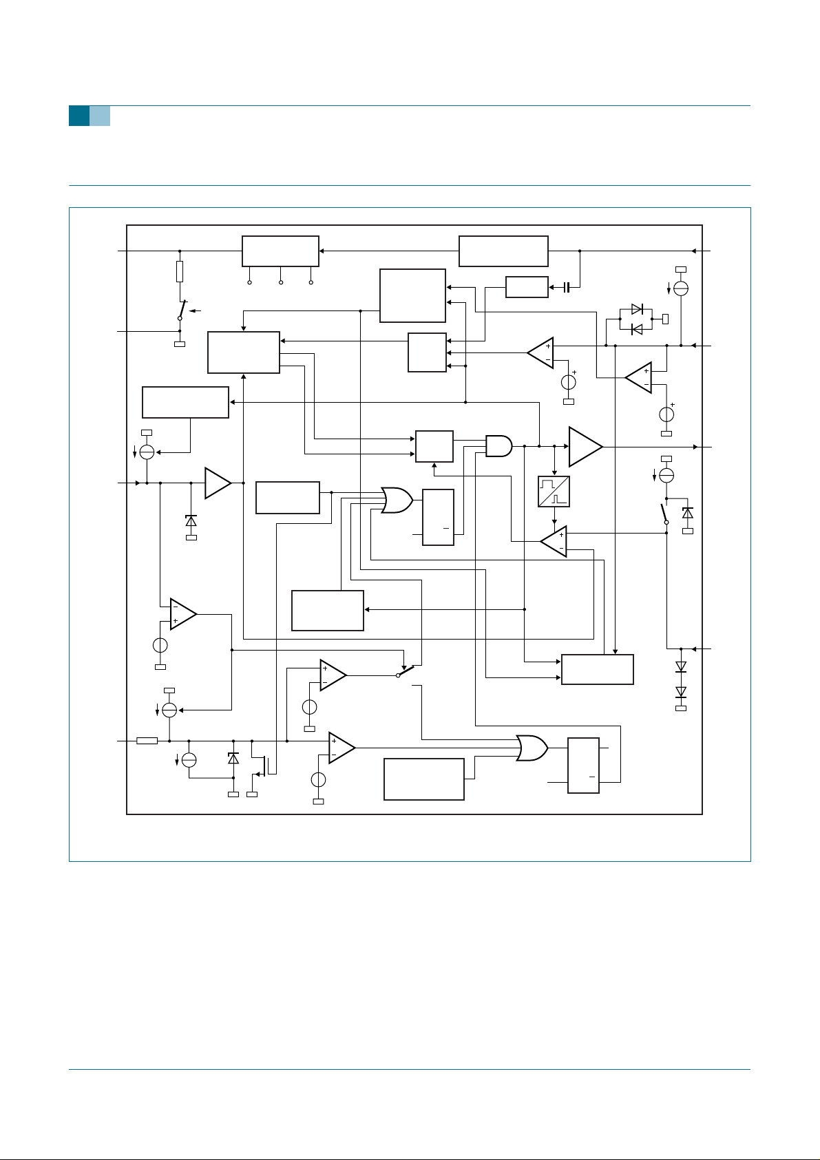
5. Block diagram
TEA1532
GreenChipII SMPS control IC
V
CC
GND
CTRL
1
S1
2
SLOPE
COMPENSATION
I
slopecomp
4
0.63 V
V
m
OSCILLATOR
−1
5.6 V
control
detect
SUPPLY
MANAGEMENT
internal
UVLO start
supply
POWER-ON
RESET
MAXIMUM
ON-TIME
PROTECTION
DETECTION
Osc_Rdy
Duty_Max
UVLO
DCM
AND
CCM
LOGIC
CURRENT SOURCE
LOGIC
SQ
R
Q
S3
START-UP
VALLEY
DCM and CCM
80
mV
DRIVER
LEB
blank
OCP
BROWN-OUT
PROTECTION
I
prot(dem)
clamp
soft
start
S2
−50
mV
I
ss
0.5 V
8
5
7
6
DRAIN
DEM
DRIVER
SENSE
2.5 V
I
PROTECT
3
300 Ω
I
discharge
charge
5.6 V
3 V
protect
detect
OVER-
TEMPERATURE
PROTECTION
SQ
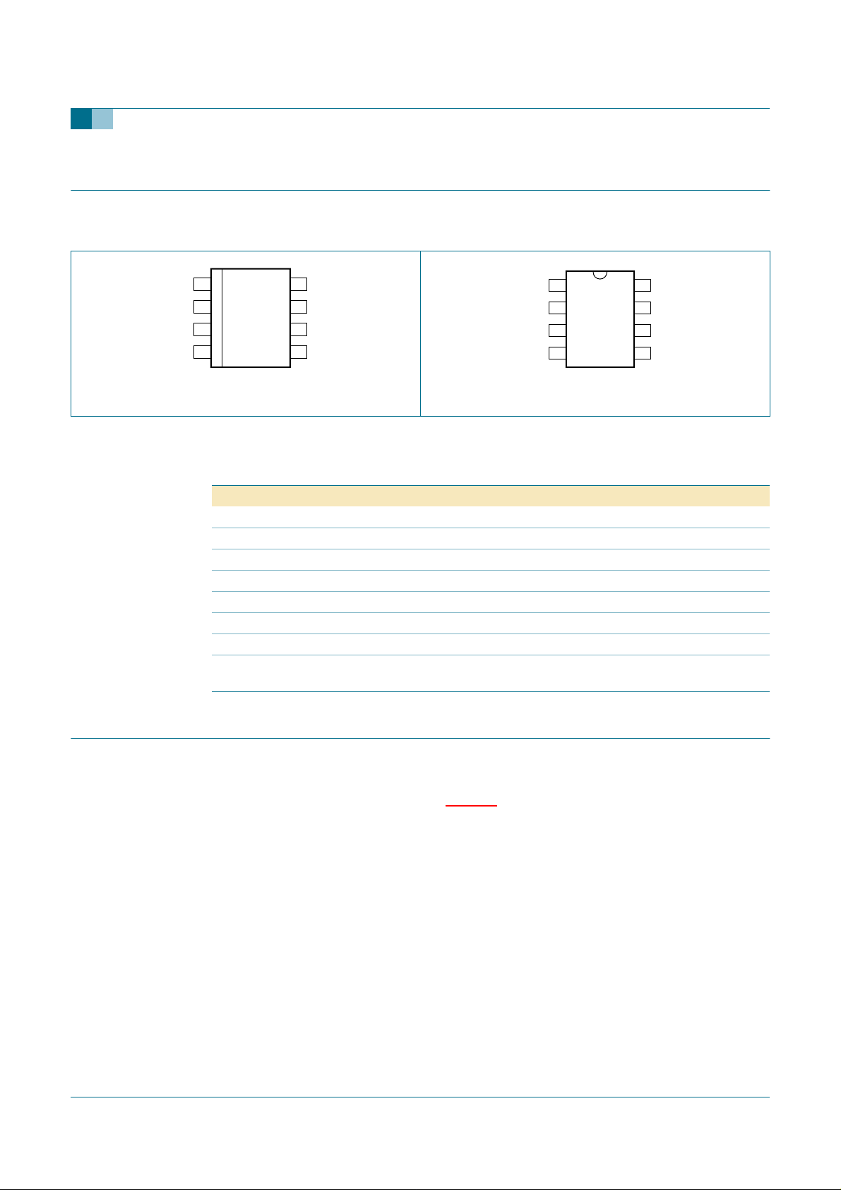
TEA1532T
TEA1532P
R
V
< 4.5 V
CC
Q
coa014
Fig 1. Block diagram.
9397 750 13113 © Koninklijke Philips Electronics N.V. 2004. All rights reserved.
Preliminary data sheet Rev. 01 — 28 May 2004 3 of 27
Philips Semiconductors
6. Pinning information
6.1 Pinning
TEA1532
GreenChipII SMPS control IC
1
V
CC
2
GND DRIVER
PROTECT SENSE
CTRL DEM
3
4
TEA1532T
001aaa829
8
7
6
5
DRAIN
1
V
CC
2
GND DRIVER
PROTECT SENSE
CTRL DEM
TEA1532P
3
4
001aaa828
8
7
6
5
DRAIN
Fig 2. Pin configuration: TEA1532T (SOT96-1). Fig 3. Pin configuration: TEA1532P (SOT97-1).
6.2 Pin description
Table 2: Pin description
Symbol Pin Description
V
CC
GND 2 ground
PROTECT 3 protection and timing input
CTRL 4 control input
DEM 5 input from auxiliary winding for demagnetization timing
SENSE 6 programmable current sense input
DRIVER 7 MOSFET Gate driver output
DRAIN 8 connected to drain of external MOS switch, input for start-up
1 supply voltage
current compensation and valley sensing
7. Functional description
The TEA1532 is the controller of a compact flyback converter, with the IC situated at the
primary side. An auxiliary winding of the transformer provides demagnetization detection
and powers the IC after start-up; see Figure 4.
9397 750 13113 © Koninklijke Philips Electronics N.V. 2004. All rights reserved.
Preliminary data sheet Rev. 01 — 28 May 2004 4 of 27
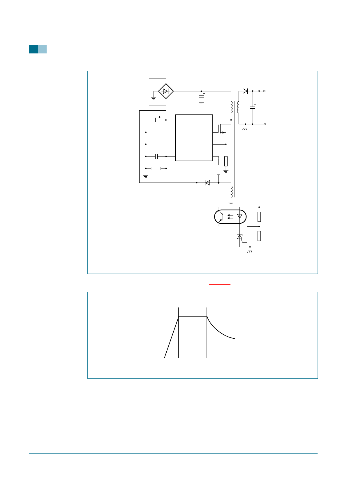
Philips Semiconductors
TEA1532
GreenChipII SMPS control IC
V
i
C
VCC
1
2
TEA1532T
TEA1532P
3
4
8
7
6
5
coa015
Fig 4. Typical configuration
The TEA1532 can operate in multi modes; see Figure 5.
f
(kHz)
63
Cycle
skip
fixed
coa017
FF-CCM
QR
P (W)
Fig 5. Multi mode and FF-CCM operation.
In QR mode, the next converter stroke is started only after demagnetization of the
transformer current (zero current switching), while the drain voltage has reached the
lowest voltage to minimize switching losses (green function). The primary resonant circuit
of primary inductance and drain capacitor ensures this quasi-resonant operation. The
design can be optimizedinsuchaway that zero voltageswitchingcan extend over most of
the universal mains range.
To prevent very high frequency operation at lower loads, the quasi-resonant operation
changes smoothly in fixed frequency Pulse Width Modulation (PWM) control.
9397 750 13113 © Koninklijke Philips Electronics N.V. 2004. All rights reserved.
Preliminary data sheet Rev. 01 — 28 May 2004 5 of 27

Philips Semiconductors
In fixed frequency continuous conduction mode, the internal oscillator determines the start
of the next converter stroke.
In both operating modes, a cycle skipping mode is activated at very low power (standby)
levels.
7.1 Start-up, mains enabling operation level and undervoltage lock out
Refer to Figure 10 and Figure 11. Initially, the IC is self supplying from the rectified mains
voltage via pin DRAIN. Supply capacitor C
current source to a level of about 4 V or higher, depending on the drain voltage. Once the
drain voltage exceeds the Vm (mains-dependent operation-enabling level), the start-up
current source will continue charging capacitor C
Figure 1. The IC will activate the power converter as soon as the voltage on pin V
passes the V
output voltage reaches its intended level and the IC supply from the mains voltage is
subsequently stopped for high efficiency operation (green function).
TEA1532
GreenChipII SMPS control IC
(at pin 1) is charged by the internal start-up
VCC
(switch S1 will be opened); see
VCC
level.The IC supply is taken over by the auxiliary winding as soon as the
start
CC
The moment the voltage on pin VCC drops below V
(undervoltage lock out), the IC
UVLO
stops switching and enters a safe restart from the rectified mains voltage. Inhibiting the
auxiliary supply by external means causes the converter to operate in a stable,
well-defined burst mode.
7.2 Supply management
All (internal) reference voltages are derived from a temperature compensated, on-chip
band gap circuit.
7.3 Current control mode
Current control mode is used for its good line regulation behavior.
The on-time is controlled by the internally inverted pin CTRL voltage, which is compared
with the primary current information. The primary current is sensed across an external
resistor. The driver output is latched in the logic, preventing multiple switch-on.
The internal control voltage is inversely proportional to the external pin CTRL voltage, with
an offset of 1.5 V. This means that a voltage range from 1 V to approximately 1.5 V on
pin CTRL will result in an internal control voltage range from 0.5 V to 0 V (a high external
control voltage results in a low duty cycle).
V
sense(max)
coa016
0.52 V
Cycle
skip
active
25 mV
1 V
(typ)
Fig 6. The V
9397 750 13113 © Koninklijke Philips Electronics N.V. 2004. All rights reserved.
Preliminary data sheet Rev. 01 — 28 May 2004 6 of 27
sense(max)
voltage as a function of V
1.5 V
CTRL
(typ)
.
V
CTRL

Philips Semiconductors
7.4 Oscillator
The fixed frequency of the oscillator is set by an internal current source and capacitor.
7.5 Cycle skipping
At very low power levels, a cycle skipping mode activates. An internal control voltage
(V
sense(max)
this voltage increases to a higher value; see Figure 6.
7.6 Demagnetization (QR operation)
The system will be in Discontinuous Conduction Mode (DCM) (QR operation) when
resistor R
secondary stroke has ended.
Demagnetization features a cycle-by-cycle output short-circuit protection which
immediately reduces the frequency (longer off-time), thereby reducing the power level.
TEA1532
GreenChipII SMPS control IC
) lower than 25 mV will inhibit switch-on of the external power MOSFET until
is applied. The oscillator will not start a new primary stroke until the
DEM
Demagnetization recognition is suppressed during the first t
may be necessary in applications where the transformer has a large leakage inductance
and at low output voltages or start-up.
time. This suppression
supp
7.7 Continuous Conduction Mode (CCM)
It is also possible to operate the IC in the so-called Fixed Frequency Continuous
Conduction Mode (FF CCM). This mode is activated by connecting pin DEM to ground
and connecting pin DRAIN to the rectified constant Vi voltage; see Figure 13.
7.8 Overcurrent Protection (OCP)
The current in the transformer primary is measured accurately by the internal
cycle-by-cycle source current limit circuit using the external sense resistor R
The accuracy of the current limit circuit allows the transformer core to have a minimum
specification forthe output power required. The OCP circuit limits the ‘sense’ voltage to an
internal level, and is activated after the leading edge blanking period, t
Leading Edge Blanking (LEB) circuit.
generated by the
leb
7.9 Control pin protection
If pin CTRL becomes open-circuit or is disconnected, a fault condition is assumed and the
converter will stop operating immediately. Operation recommences when the fault
condition is removed.
sense
.
7.10 Adjustable slope compensation
A slope compensation function has been added at pin CTRL; see Figure 7. The slope
compensation function prevents sub-harmonic oscillation in CCM at duty cycles over
50 %. The CTRL voltage is modulated by sourcing a (non-constant) current out of
pin CTRL and adding a series resistor R
proportionally with the on-time, which therefore limits the OCP level. Thus, a longer
on-time results in a higher CTRL voltage, however, this increase in CTRL voltage will
actually decrease the on-time. Slope compensation can be adjusted by changing the
9397 750 13113 © Koninklijke Philips Electronics N.V. 2004. All rights reserved.
Preliminary data sheet Rev. 01 — 28 May 2004 7 of 27
slopecomp
. This increases the CTRL voltage

Philips Semiconductors
TEA1532
GreenChipII SMPS control IC
value of R
slopecomp
. Slope compensation prevents modulation of the on-time (duty cycle)
while operating in FF CCM. A possible drawback of sub-harmonic oscillation can be
output voltage ripple.
TEA1532
Slope compensation
current
R
R
CTRL
Fig 7. Slope compensation.
slopecomp
CTRL
4
−1
5.6 V
control
detect
0.63 V
001aaa830
7.11 Minimum and maximum on-time
The minimum on-time of the SMPS is determined by the LEB time. The IC limits the
on-time to a maximum time which is dependent on the mode of operation:
QR mode: When the system requires an ‘on-time’ of more than 25 µs, a fault condition is
assumed (e.g. C
removed), the IC stops switching and enters the safe restart mode.
VCC
CCM: The driver duty cycle is limited to 70 %. So the maximum on-time is correlated to
the oscillator time which results in an accurate limit of the minimum input voltage of the
flyback converter.
7.12 PROTECT and timing input
The PROTECT input (pin 3) is a multi-purpose (high-impedance) input, which can be used
to switch off the IC and create a relatively long timing function. As soon as the voltage on
this pin rises above 2.5 V, switching stops immediately. For the timing function, a current of
typically 50 µA flows out of pin PROTECT and charges an external capacitor until the
activation level of 2.5 V is reached. This current source however, is only activated when
the converter is not in regulation, which is detected by the voltage on pin CTRL
(V
capacitor is not charged, for example, by spikes, and a MOSFET switch is added to
ensure a defined start situation. The voltage on pin CTRL determines whether the IC
enters latched protection mode, or safe restart protection mode:
< 0.63 V). A (small) discharge current is also implemented to ensure that the
CTRL
9397 750 13113 © Koninklijke Philips Electronics N.V. 2004. All rights reserved.
Preliminary data sheet Rev. 01 — 28 May 2004 8 of 27

Philips Semiconductors
p
--
• When the voltage on pin CTRL is below 0.63 V, the IC is assumed to be out of
regulation (e.g. the control loop is open). In this case activating pin PROTECT
(V
V
UVLO
repeated until the fault condition is removed (safe restart mode)
• Whenthe voltage on pin CTRL is above 0.63 V, the IC is assumed to be in regulation.
In this case activating pin PROTECT(V
the IC: The voltage on pin VCC will cycle between V
start switching again until the latch function is reset. The latch is reset as soon as V
drops below 4.5 V (typical value). The internal overtemperature protection will also
trigger this latch; see also Figure 1.
A voltagehigher than 3 V on pin PROTECTwill always latch the IC. This is independent of
the state of the IC.
7.13 Valley switching
Refer to Figure 8. A new cycle starts when the power switch is activated. After the on-time
(determined by the sense voltage and the internal control voltage), the switch is opened
and the secondary stroke starts. After the secondary stroke, the drain voltage shows an
oscillation with a frequency of approximately
PROTECT
, capacitor C
TEA1532
GreenChipII SMPS control IC
> 2.5 V) will cause the converter to stop switching. Once VCC drops below
will be recharged and the supply will restart. This cycle will be
VCC
PROTECT
> 2.5 V), by external means, will latch
and V
start
-----------------------------------------------
2 π× L
1
Cd×()×(
, but the IC will not
UVLO
CC
where Lp is the primary self inductance of the transformer and Cd is the capacitance on
the drain node.
As soon as the oscillator voltage is high again and the secondary stroke has ended, the
circuit waits for the lowest drain voltage before starting a new primary stroke. This method
is called valley detection. Figure 8 shows the drain voltage, valley signal, secondary stroke
signal and the oscillator signal.
In an optimum design, the reflected secondary voltage on the primary side will force the
drain voltage to zero. Thus, zero voltage switching is possible, preventing large capacitive
1
switching losses , and allowing high frequency operation, which
P
-- -
2
2
CV
× f××=
results in small and cost effective magnetics.
9397 750 13113 © Koninklijke Philips Electronics N.V. 2004. All rights reserved.
Preliminary data sheet Rev. 01 — 28 May 2004 9 of 27
 Loading...