

Philips TEA1506 Service Manual

INTEGRATED CIRCUITS
DATA SH EET
TEA1506P;TEA1506T
GreenChip
Preliminary specification
File under Integrated Circuits, IC11
TM
II SMPS control IC
2002 Sep 04
Philips Semiconductors Preliminary specification
GreenChipTMII SMPS control IC
FEATURES
Distinctive features
• Universal mains supply operation (70 to 276 V AC)
• High level of integration, giving a low external
component count.
Green features
• Valley or zero voltage switching for minimum switching
losses
• Efficient quasi-resonant operation at high power levels
• Frequency reductionat low power standby for improved
system efficiency (<3 W)
• Cycle skipping mode at very low loads.
Protection features
• Safe restart mode for system fault conditions
• Continuous mode protection by means of
demagnetization detection (zero switch-on current)
• Accurate and adjustable overvoltage protection
• Short winding protection
• Undervoltage protection (foldback during overload)
• Overtemperature protection
• Low and adjustable overcurrent protection trip level
• Soft (re)start
TEA1506P;TEA1506T
APPLICATIONS
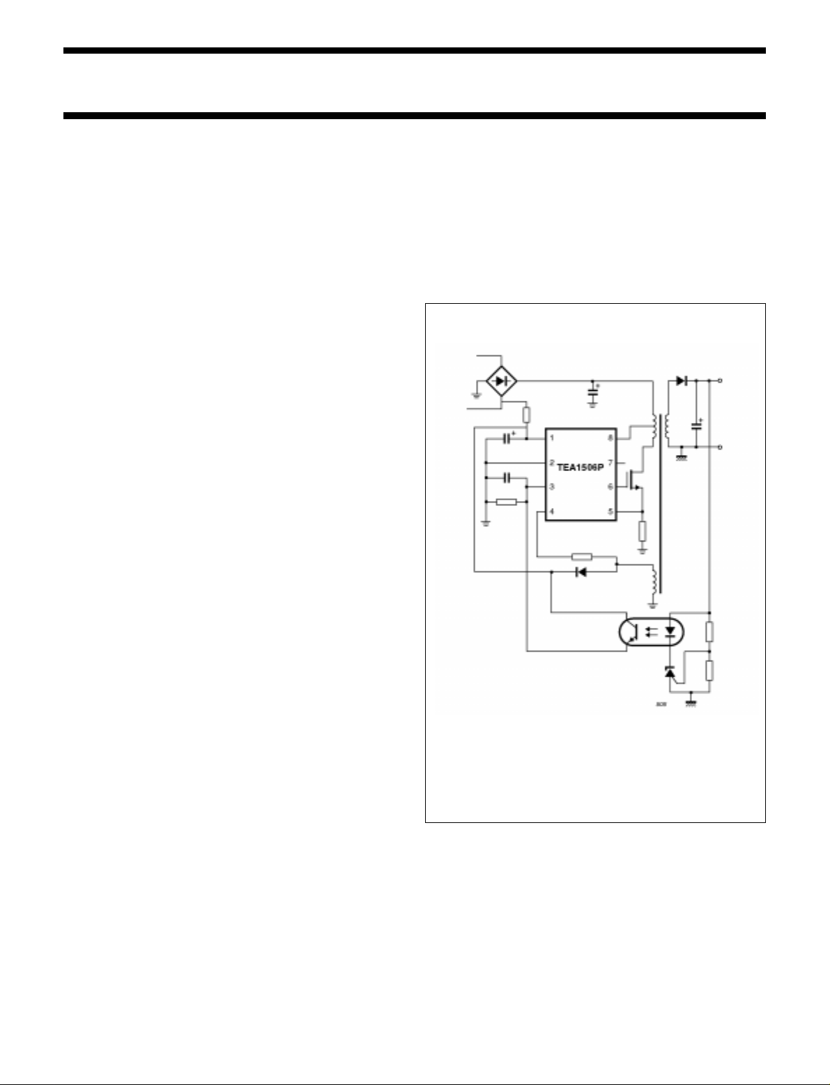
Besides typical application areas, i.e. TV and monitor
supplies,the device canbe used in adaptersand chargers
and all applications that demand an efficient and
cost-effective solution up to 150 W. Unlike the other
GreenchipTMII control ICs, the TEA1506 has no internal
high voltage start-up source and needs to be started by
means of an external bleeder resistor.
2002 Sep 04 2
Fig.1 Basic application diagram.
Philips Semiconductors Preliminary specification
GreenChipTMII SMPS control IC
GENERAL DESCRIPTION
The GreenChip
Switched Mode Power Supply (SMPS) control ICs. A high
level of integration leads to a cost effective power supply
with a low number of external components.
The special built-in green functions allow a high efficiency
atall power levels.This holds forquasi-resonant operation
at high power levels, as well as fixed frequency operation
withvalleyswitching at medium powerlevels.Atlow power
(standby) levels, the system operates at a reduced
frequency and with valley detection.
(1) GreenChip is a trademark of Koninklijke Philips
Electronics N.V.
ORDERING INFORMATION
TYPE NUMBER
TEA1506P DIP8 plastic dual in-line package; 8 leads (300 mil) SOT97-1
TEA1506T SO14 plastic small outline package; 14 leads SOT108
(1)
II is the second generation of green
NAME DESCRIPTION VERSION
Highly efficient and reliable supplies can easily be
designed using the GreenChipII control IC.
PACKAGE
TEA1506P;TEA1506T
2002 Sep 04 3
This text is here in white to force landscape pages to be rotated correctly when browsing through the pdf in the Acrobat reader.This text is here in
_white to force landscape pages to be rotated correctly when browsing through the pdf in the Acrobat reader.This text is here inThis text is here in
white to force landscape pages to be rotated correctly when browsing through the pdf in the Acrobat reader. white to force landscape pages to be ...
2002 Sep 04 4
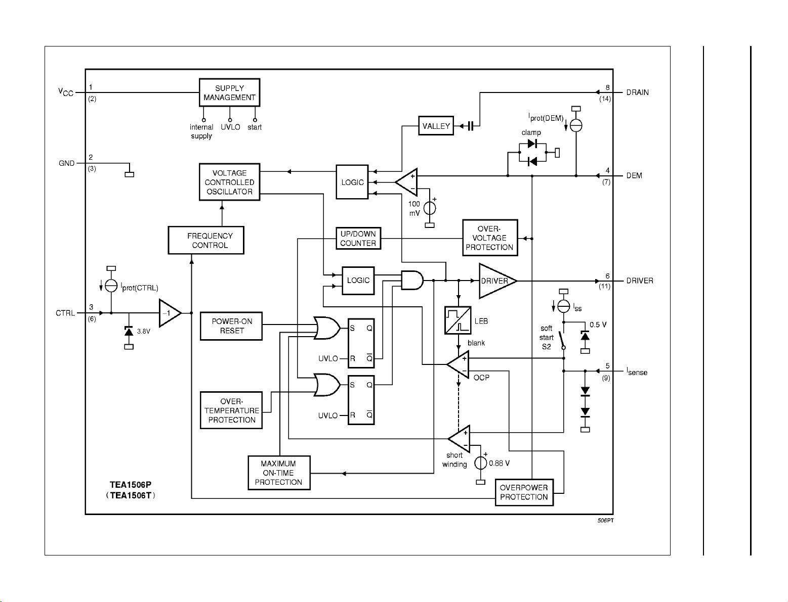
BLOCK DIAGRAM
Philips Semiconductors Preliminary specification
GreenChip
TM
II SMPS control IC
Fig.2 Block diagram.
TEA1506P;TEA1506T
Philips Semiconductors Preliminary specification
GreenChipTMII SMPS control IC
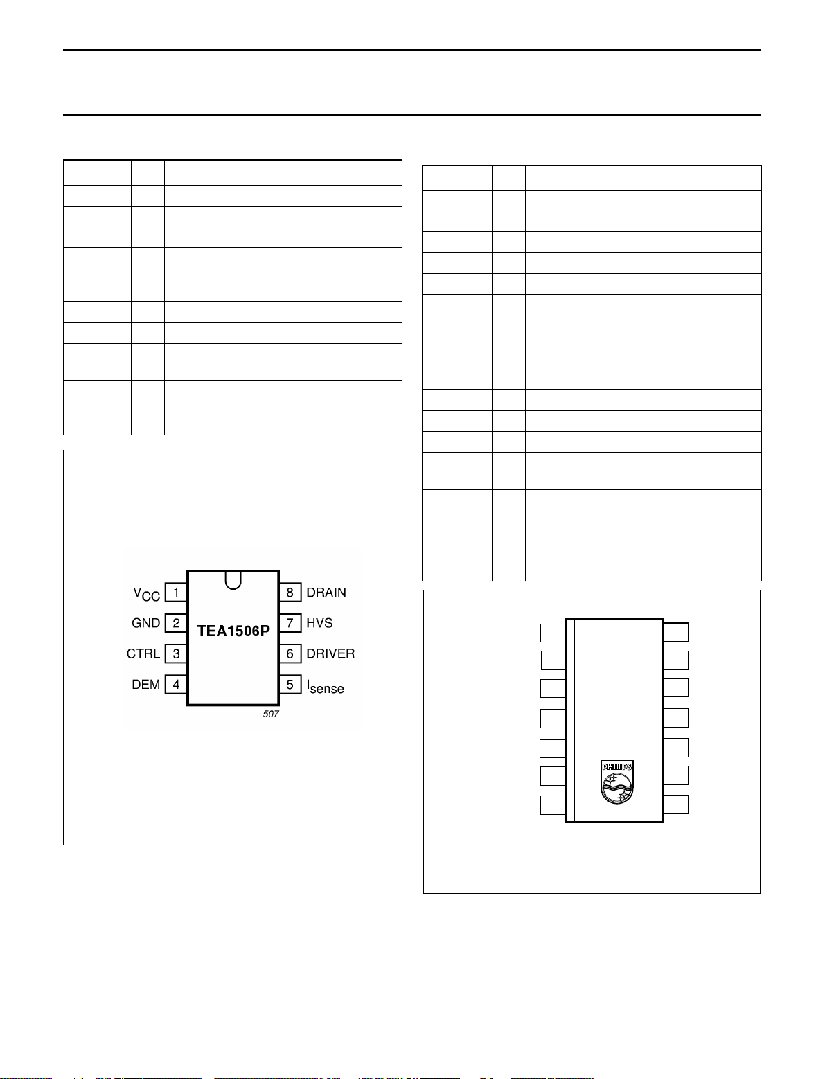
PINNING (DIP-8) PINNING (SO-14)
SYMBOL PIN DESCRIPTION
V
CC
GND 2 Ground
Ctrl 3 Control input
Dem 4 Input from auxiliary winding for
I
sense
Driver 6 Gate driver output
HVS 7 High voltage safety spacer, not
Drain 8 Drainof external MOS switch, input for
1 Supply voltage
demagnetization timing, overvoltage
and overpower protection
5 Programmable current sense input
connected
valley sensing and initial internal
supply
SYMBOL PIN DESCRIPTION
Nc 1 Not Connected
Vcc 2 Supply voltage
GND 3 Ground
Nc 4 Not Connected
Nc 5 Not Connected
Ctrl 6 Control input
Dem 7 Input from auxiliary winding for
Nc 8 Not Connected
I
sense
Nc 10 Not Connected
Driver 11 Gate driver output
HVS 12 High Voltage safety Spacer, not
HVS 13 High Voltage safety Spacer, not
Drain 14 Drain of external MOS switch,input for
9 Programmable current sense input
TEA1506P;TEA1506T
demagnetization timing, overvoltage
and overpower protection
connected
connected
valley sensing and initial internal
supply
Fig.3 Pin configuration.
Nc
1
Vcc
Gnd
Nc
Nc
Ctrl
Dem
Fig.4 Pin configuration SO-14
2
3
4
5
6
7
TEA1506T
14
13
12
11
10
9
8
Drain
HVS
HVS
Driver
Nc
Isense
Nc
2002 Sep 04 5
Philips Semiconductors Preliminary specification
GreenChipTMII SMPS control IC
FUNCTIONAL DESCRIPTION
The TEA1506 is the controller of a compact flyback
converter, and is situated at the primary side. An auxiliary
winding of the transformer provides demagnetization
detection and powers the IC after start-up.
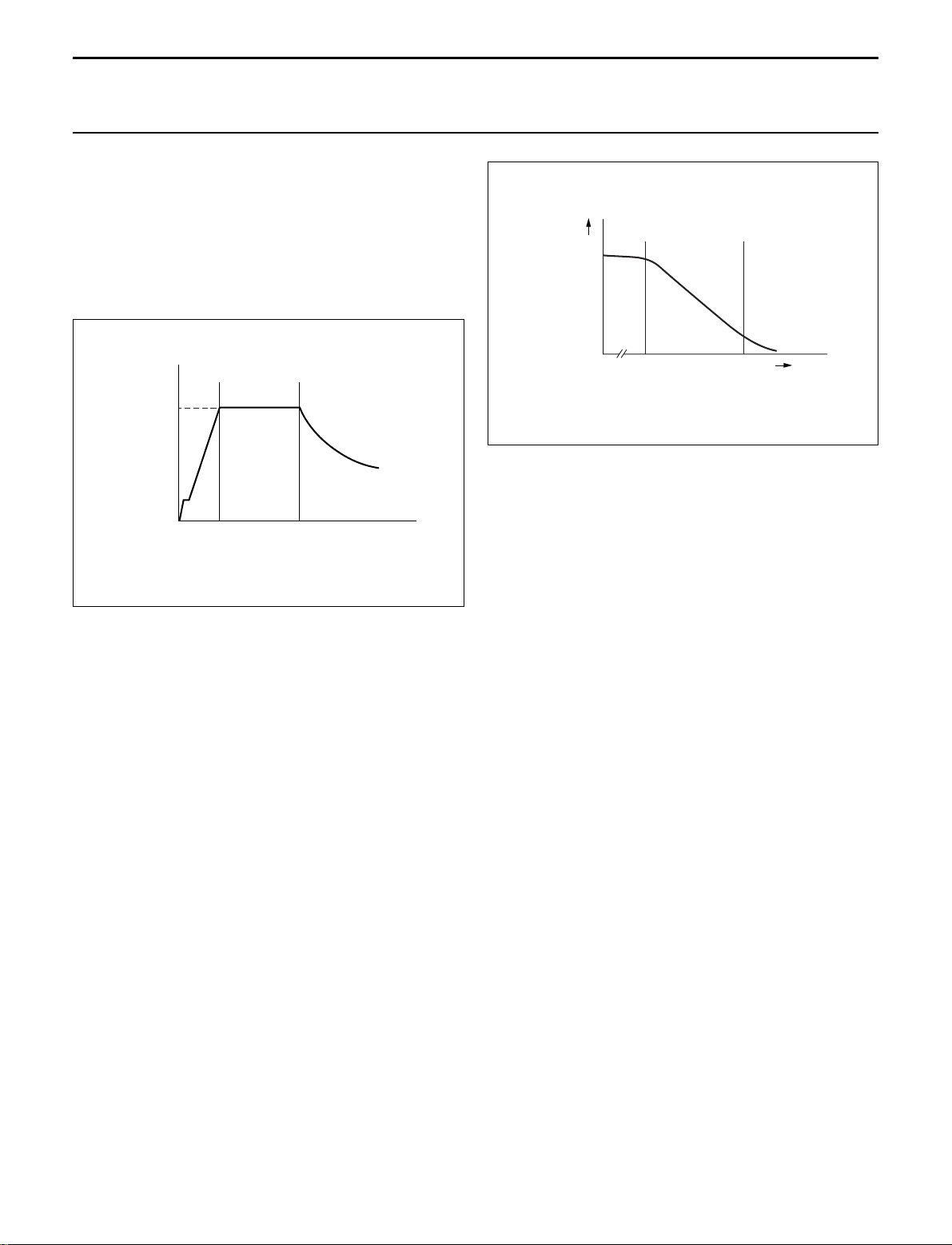
The TEA1506 can operate in multi modes (see Fig.5).
handbook, halfpage
(kHz)
f
VCO fixed quasi resonant
175
25
MGU508
P (W)
TEA1506P;TEA1506T
V
handbook, halfpage
sense(max)
Fig.6 V
0.5 V
sense(max)
1 V
(typ)
1.5 V
(typ)
voltage as function of V
The moment the voltage on pin VCC drops below the
undervoltage lock-out level, the IC stops switching and
re-enters the safe restart mode.
Supply management
MGU233
V
CTRL
CTRL
.
Fig.5 Multi modes operation.
The next converter stroke is started only after
demagnetization of the transformer current (zero current
switching), while the drain voltage has reached the lowest
voltage to prevent switching losses (green function). The
primary resonant circuit of the primary inductance and
draincapacitorensuresthis quasi-resonant operation. The
design can be optimized in such a way that zero voltage
switching can be reached over almost the universal mains
range.
To prevent very high frequency operation at lower loads,
the quasi-resonant operation changes smoothly in fixed
frequency PWM control.
At very low power (standby) levels, the frequency is
controlled down, via the VCO, to a minimum frequency of
approximately 25 kHz.
Start-up and undervoltage lock-out
Initially the IC is in the save restart mode. As long as V
is below the V
level, the supply current is nearly
CC(start)
CC
zero.
TheIC will activate theconverteras soon as thevoltageon
pin VCC passes the V
CC(start)
level.
The IC supply is taken over by the auxiliary winding as
soon as the output voltage reaches its intended level.
All (internal) reference voltages are derived from a
temperature compensated, on-chip band gap circuit.
Current mode control
Current mode control is used for its good line regulation
behaviour.
The ‘on-time’ iscontrolled by theinternally inverted control
voltage, which is compared with the primary current
information. The primary current is sensed across an
external resistor. The driver output is latched in the logic,
preventing multiple switch-on.
The internal control voltage is inverselyproportional to the
external control pin voltage, with an offset of 1.5 V. This
means that a voltage range from 1 to 1.5 V on pin CTRL
will result in an internal control voltage range from
0.5 to 0 V (a high external control voltage results in a low
duty cycle).
Oscillator
The maximum fixed frequency of the oscillator isset by an
internal current source and capacitor. The maximum
frequency is reduced once the control voltage enters the
VCO control window. Then, the maximum frequency
changeslinearly with thecontrol voltage untilthe minimum
frequency is reached (see Figs 6 and 7).
2002 Sep 04 6
Philips Semiconductors Preliminary specification
GreenChipTMII SMPS control IC
handbook, halfpage
f
(kHz)
175
25
VCO
level
VCO
1
2
level
Fig.7 VCO frequency as function of V
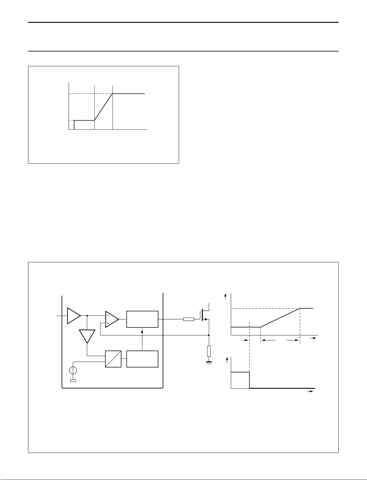
Cycle skipping
At very low power levels, a cycle skipping mode will be
activated. A high control voltage will reduce the switching
frequency to a minimum of 25 kHz. If the voltage on the
control pin is raised even more, switch-on of the external
power MOSFET will be inhibited until the voltage on the
control pin has dropped to a lower value again (see Fig.8).
MGU509
175 kHz
V
sense(max) (V)
sense(max)
TEA1506P;TEA1506T
Remark: If the no-load requirement of the system is such
that the output voltage can be regulated to its intended
level at a switching frequency of 25 kHz or above, the
cycle skipping mode will not be activated.
For system accuracy, it is not the absolute voltage on the
control pin that will trigger the cycle skipping mode, but a
signal derived from the internal VCO will be used.
handbook, full pagewidth
CTRL
1.5 V − V
CTRL
X2
V
x
150 mV
current
comparator
V
I
DRIVER
OSCILLATOR
DRIVER
I
sense
f
osc
f
max
f
min
cycle
skipping
1
0
dV
2
dV
1
150
Vx (mV)
MGU510
Vx (mV)
The voltage levels dV1 and dV2 are fixed in the IC to 50 mV (typical) and 18 mV (typical) respectively.
Fig.8 The cycle skipping circuitry.
2002 Sep 04 7
 Loading...