


INTEGRATED CIRCUITS
DATA SH EET
TEA1504
GreenChip; SMPS control IC
Preliminary specification
File under Integrated Circuits, IC11
1998 Mar 17
Philips Semiconductors Preliminary specification
GreenChip; SMPS control IC TEA1504
PRODUCT HIGHLIGHTS
Distinctive features
• High level of integration leads to 20 to 50 fewer
components compared to power supply with discrete
components
• On-chip efficient startup current source giving fast
startup
• ON/OFF function replaces expensive mains switch with
functional switch
• Direct off-line operation (90 to 276 Vac)
• On-chip 5% accurate oscillator.
Green features
• Low power consumption in off-mode (<100 mW)
• Burst mode stand-by (<2 W) for overall improved
system efficiency
• Low power operation mode with lower frequency to
reduce switching losses.
Protection features
• Demagnetization protection
• Cycle by cycle current limitation with programmable
current trip level
• Accurate over voltage protection which tracks the output
voltage
• Over temperature protection
• Safe-restart mode with reduced power for system fault
conditions.
Highly versatile
• Usable in Buck and Flyback topology
• Interfaces both primary and secondary side feedback.
Output
OOB
14
Dem
13
12
NC
11
Gnd
NC
10
Vctrl
9
Iref
8
Vin
NC
NC
Driver
Isense
Vaux
1
2
3
4
5
6
7
DS
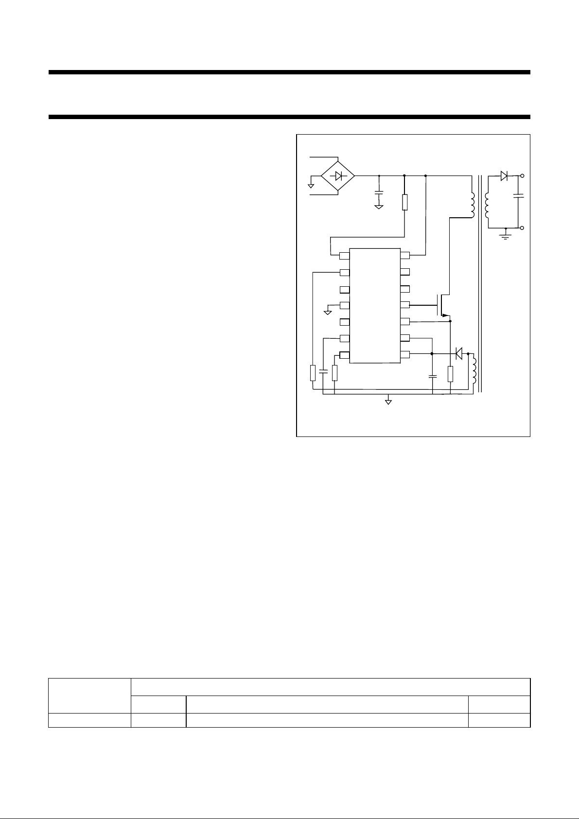
Fig.1 Typical Flyback Application.
GENERAL DESCRIPTION
The GreenChip, intended for off-line 90 to 276 Vac
power supply applications, is a monolithic high voltage
family of ICs that combines analog and digital circuits to
implement all necessary control functions for a switched
mode power supply. The functions include integrated high
voltage startup current source, voltage mode PWM
control, 5% accurate trimmed oscillator, bandgap derived
reference voltages, comprehensive fault protection, and
leading edge blanking. High level of integration leads to
cost effective power supplies that are compact, weigh less,
and at the same time give higher efficiency, are more
reliable and simple to design. Efficient green features lead
to very low power operation modes and a novel ON/OFF
function helps replace the expensive mains switch with a
low cost functional switch.
ORDERING INFORMATION
PACKAGE
TYPE NUMBER
NAME DESCRIPTION VERSION
TEA1504 DIP14 plastic dual in-line package; 14 leads (300 mil) SOT27-1
1998 Mar 17 2

Philips Semiconductors Preliminary specification
GreenChip; SMPS control IC TEA1504
FUNCTIONAL BLOCK DIAGRAM
OOB
14
5.5V
Vctrl
9
Dem
13
On/Off
Iref
-
+
Burst mode
stand-by
Sample &
Hold 1
Demag
Mgmnt
Vaux
8
Vaux management
+
-
Over temp
protection
Sample &
Hold 2
6
Error
Amp.
Oscillator
PWM
Comp.
+
-
Vin
Startup current
source
1
R
S
* Over current
protection
* Leading Edge
blanking
Frequency control
TEA1504
Q
DS
7
Driver
4
Isense
5
Negative
Clamp
Gnd
Fig.2 Functional Block Diagram.
1998 Mar 17 3
11
NC pins: 2, 3, 10 & 12

Philips Semiconductors Preliminary specification
GreenChip; SMPS control IC TEA1504
PINNING
SYMBOL PIN DESCRIPTION
Vin 1 MOSFET Drain connection
HVS 2 High voltage safety spacer
NC 3 Not connected
Driver 4 MOSFET gate driver output
Isense 5 Programmable current
sense resistor
Vaux 6 IC supply capacitor
DS 7 Supply for driver circuit
Iref 8 Reference resistor for
setting internal reference
currents
Vctrl 9 Feedback voltage for duty
cycle control
NC 10 Not connected
Gnd 11 Ground
NC 12 Not connected
Dem 13 Demagnetization input
signal from primary side
auxiliary winding
OOB 14 On/Off/Burst Mode input
signal
Vin
HVS
NC
Driver
Isense
Vaux
DS
1
2
3
TEA1504
4
5
6
7
Fig.3 Pin assignment.
14
13
12
11
10
OOB
Dem
NC
Gnd
NC
Vctrl
9
Iref
8
FUNCTIONAL DESCRIPTION
The GreenChip family of ICs are highly integrated, with
most common PWM functions like error amplifier,
oscillator, bias current generator, and band gap based
reference voltage circuits fully integrated in the ICs.
High level of integration leads to easy and cost effective
design of power supplies. The ICs have been fabricated in
a Philips proprietary high voltage BCDMOS process that
enables devices of up to 650 V to be fabricated on the
same chip with low voltage circuitry.
An efficient on-chip startup circuit enables fast startup and
dissipates negligible power after start up. On-chip
accurate oscillator generates a saw tooth waveform which
is used by the voltage mode feedback control circuitry to
generate a pulse width modulated signal for driving the
gate of the power MOSFET. A novel regulation scheme is
used to implement both primary and secondary side
regulation to minimize external component count.
Protection features like over voltage, over current, over
temperature, and demagnetization protection, give
comprehensive safety against system fault conditions.
The GreenChip offers some advanced features that
greatly enhance the efficiency of the overall system.
Off-mode reduces the power consumption of the IC below
100 mW. Burst mode stand-by reduces the power
consumption of the system to below 2 W. Low power
operation mode reduces the operating frequency of the
system, when the system is working under low load
conditions, to reduce the switching losses.
Startup current source and vaux management
A versatile on-chip startup current source makes an
external, highly dissipative, trickle-charge circuit
unnecessary. Refer to Fig.2 for a block diagram of the IC.
The startup current source derives power from the mains
via the Vin (drain) pin. It supplies current (see Istart-low
and Istart-high in Chapter “Characteristics”) to charge the
Vaux (IC supply) capacitor and at the same time provides
current to the control circuitry of the IC. Once the Vaux
capacitor is charged to its startup voltage level (11 V), the
on chip oscillator starts oscillating and the IC starts
switching the power MOSFET. Power is then supplied to
the load via the secondary winding. Figure 1 shows a
typical flyback application diagram. The Vaux capacitor is
also supplied by an auxiliary winding on the primary side.
This winding is coupled to the secondary side winding
1998 Mar 17 4
Philips Semiconductors Preliminary specification
GreenChip; SMPS control IC TEA1504
supplying the output capacitor. As the output capacitor
voltage increases and approaches its nominal value, the
re-supply of the Vaux capacitor is done by the auxiliary
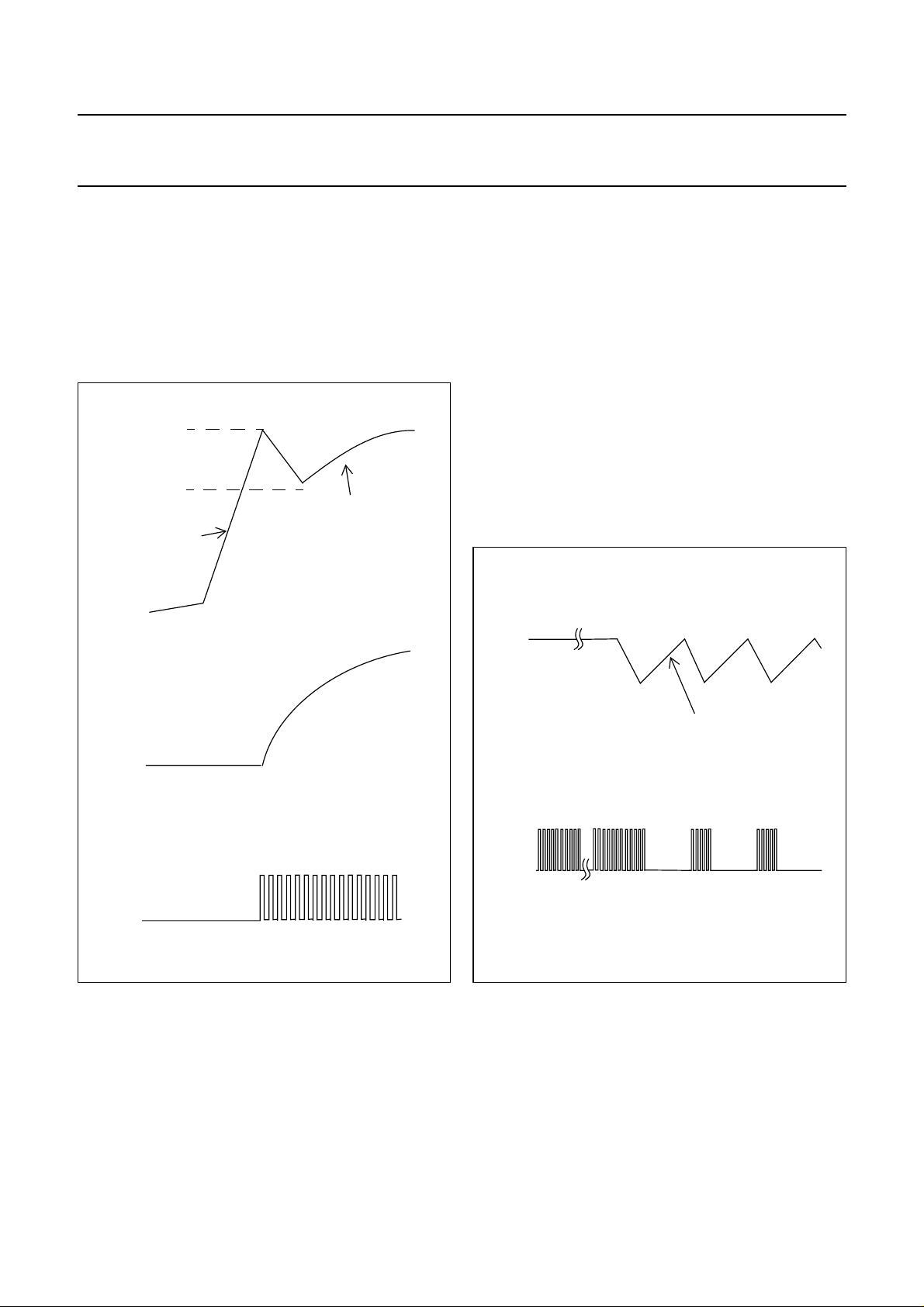
winding. Figure 4 shows relevant waveforms at startup.
For successful take over of supply of Vaux capacitor by the
auxiliary winding, it is important that the re-supply of Vaux
capacitor starts before its voltage drops to its Under
Voltage Lockout (UVLO) level of 8.15 V.
Vaux
11V
8.15V
Istartup charging
Vaux cap
charging of Vaux cap
taken over by Auxiliary
Winding
circuit, the output voltage will rise till it reaches the OVP
level. The IC will detect this state and stop switching.
In absence of switching of the power device, the Vaux
capacitor will not be re-supplied and its voltage will drop till
it reaches UVLO level. Once the Vaux voltage drops to
UVLO level, the startup current source is re-activated and
it charges the Vaux capacitor to its start level and the
system goes through a cycle similar to the startup cycle.
Figure 5 shows the relevant waveforms during safe-restart
mode. The charging current (see Irestart-prot in
Chapter “Characteristics”) from the startup circuit during
the safe-restart mode is lower than the normal startup
current (see Istart-high in Chapter “Characteristics”) in
order to implement a low “hiccup” duty cycle. This helps
insure devices on the output secondary winding do not get
destroyed during output short circuit, violating safety
conditions.
Vaux
Normal operation
Fault condition
Vout
Vgate
Off
Fig.4 Normal startup waveforms.
The startup current source also helps implement the
safe-restart or “hiccup” mode during system fault
conditions like output short circuit, output open circuit, and
Over Voltage Protection (OVP). In all the above fault
situations, the IC reacts by inhibiting the normal operation
of the system and stops delivering power to the output.
In case of output short circuit, the Vaux capacitor is no
longer supplied by the auxiliary winding and its voltage
drops till it reaches the UVLO level. If the output is an open
Switching
Startup current source
charging Vaux capacitor
Vgate
Switching
Off
Fig.5 Safe-restart mode waveforms.
The startup current source also plays a key role in
implementation of burst mode stand-by (see Irestart-stdby
in Chapter “Characteristics”), which will be explained later.
All reference voltages are derived from a temperature
compensated, on-chip, band-gap. The bandgap reference
voltage is also used, together with an external resistor
connected at the Iref pin, to generate accurate,
temperature independent, bias currents in the chip.
1998 Mar 17 5

Philips Semiconductors Preliminary specification
GreenChip; SMPS control IC TEA1504
Sample and Hold
GreenChip ICs employ voltage mode feedback for
regulating the output voltage. In primary feedback mode,
a novel Sample and Hold circuit is used. The Sample and
Hold circuit works by sampling the current into the demag
pin, which is related to the output voltage via Rdem, during
the time that the secondary current is flowing:
V
out=Iref
× R
dem+Vdem+
This sampled current information is stored on the external
capacitor connected to the Vctrl pin. The pulse width
modulator uses this voltage information to set the duty
cycle of operation for the power MOSFET. In secondary
feedback, the feedback voltage is provided by an
opto-coupler.
Pulse Width Modulator
The pulse width modulator, which is made up of an
inverting error amplifier and a comparator (Fig.2), drives
the power MOSFET with a duty cycle which is inversely
proportional to the voltage at the Vctrl pin. In primary
feedback, this is the voltage on the Sample and Hold
capacitor and in secondary feedback, this voltage is
provided by an opto-coupler. A signal from the oscillator
sets a latch that turns on the power MOSFET. The latch is
reset by the signal from the pulse width modulator or by the
duty cycle limiting circuit. The latching PWM mode of
operation prevents multiple switching of the power switch.
The maximum duty cycle is set internally at 80%. Figure 6
shows the normal switching operation of the IC.
Oscillator
The oscillator is used to set the switching duty cycle by
comparing the oscillator ramp to the output of the error
amplifier in the pulse width modulator circuit. The oscillator
is fully integrated and works by charging and discharging
an internal capacitor between two voltage levels to create
a sawtooth waveform with a rising edge which is 80% of
the oscillator cycle. This ratio is used to set a maximum
switching duty cycle of 80% for the IC. The oscillator is
internally trimmed to 5% accuracy. The oscillator
frequency can be adjusted between 49 to 91 kHz
(see f
osc-h-range
in Chapter “Characteristics”) by changing
the external reference resistor (see Rref in
Chapter “Characteristics”) that sets the chip bias currents.
This gives additional flexibility to the power supply
designer in the choice of his system components.
The frequency is correlated with the value of the Rref
resistor:
f
oscfosc typical–
f
osc-typical
and f
osc-h
is specified in Chapter “Characteristics”, f
. The operating Rref resistor range is specified in
24.900
× Hz[]=
-----------------Rref
osc-l
Chapter “Characteristics”, Rref.
Multi Frequency Control
The oscillator is also capable of working at a lower
frequency (see f
in Chapter “Characteristics”). A ratio
osc-l
of 1 : 2.5 is maintained between high and low frequency of
the oscillator. Low frequency operation is invoked if the
power supply is working at or below one ninth of its peak
power. By working at a lower frequency, the switching
losses in the power supply are reduced. A novel scheme
is used to ensure that the transfer of high to low frequency
and vice versa has no effect on the regulation of the output
voltage.
Gate Driver
The gate driver has a totem-pole output stage that has
current sourcing capability of 120 mA and a current sink
capability of 500 mA. This is to enable fast turn on and turn
off of the power device for efficient operation. In the DIL14
controller version, the driver supply and driver output pins
are available separately to the power supply designer.
In this way the power supply designer can control the
source and sink currents of the gate driver circuit with a
minimum of external components.
Demagnetization Protection
This feature guarantees discontinuous conduction mode
operation for the power supply which simplifies the design
of feedback control and gives faster transient response.
Demagnetization protection is an additional protection
feature that protects against saturation of the
transformer/inductor. Demagnetization protection also
protects the power supply components against excessive
stresses at startup, when all energy storage components
are completely discharged, and during shorted output
system fault condition.
Negative Clamp
The negative clamp circuit does not let the voltage at the
demag pin go below −0.4 V, when the auxiliary winding
voltage goes negative during the time that the power
device is turned on, to ensure correct operation of the IC.
1998 Mar 17 6
 Loading...