

Philips TDA8767 User Manual

INTEGRATED CIRCUITS
DATA SH EET
TDA8767
12-bit high-speed Analog-to-Digital
Converter (ADC)
Preliminary specification
Supersedes data of 1997 Jun 27
File under Integrated Circuits, IC02
1999 Feb 16

Philips Semiconductors Preliminary specification
12-bit high-speed Analog-to-Digital
Converter (ADC)
FEATURES
• 12-bit resolution
• Sampling rate up to 30 MHz
•−3 dB bandwidth of 18 MHz
• No missing codes guaranteed
• 5 V power supplies
• Binary or two’s complement CMOS outputs
• In-range CMOS output
• TTL/CMOS compatible static digital inputs
• 3 to 5 V CMOS digital outputs
• TTL compatible clock input
• Power dissipation 335 mW (typ.)
• Low analog input capacitance (typ. 2 pF), no buffer
amplifier required
• No external sample-and-hold circuit required
• Differential or single analog Input
• External amplitude range control
• Voltage controlled regulator included.
TDA8767
APPLICATIONS
• High-speed analog-to-digital conversion for:
– Video signal digitizing
– High Definition TV (HDTV)
– Imaging (camera, scanner)
– Medical imaging
– Telecommunication
– Base-station receiver.
GENERAL DESCRIPTION
The TDA8767 is a bipolar 12-bit Analog-to-Digital
Converter (ADC) for imaging or other applications.
It converts the analog input signal into 12-bit binary coded
digital words at a maximum sampling rate of 30 MHz.
All digital inputs and outputs are CMOS compatible.
QUICK REFERENCE DATA
SYMBOL PARAMETER CONDITIONS MIN. TYP. MAX. UNIT
V
CCA
V
CCD
V
CCO
I
CCA
I
CCD
I
CCO
ILE integral non-linearity f
DLE differential non-linearity f
analog supply voltage 4.75 5.0 5.25 V
digital supply voltage 4.75 5.0 5.25 V
output supply voltage 3.0 3.3 5.25 V
analog supply current − 40 tbf mA
digital supply current − 22 tbf mA
output supply current f
= 4 MHz; fi= 400 kHz − 3.2 tbf mA
clk
= 4 MHz; fi= 400 kHz −±3.0 ±4.0 LSB
clk
= 4 MHz; fi= 400 kHz;
clk
−±0.6 ±1 LSB
no missing codes
f
clk(max)
maximum clock frequency
TDA8767H/1 10 −−MHz
TDA8767H/2 20 −−MHz
TDA8767H/3 30 −−MHz
P
tot
total power dissipation − 335 − mW
1999 Feb 16 2
Philips Semiconductors Preliminary specification
12-bit high-speed Analog-to-Digital
TDA8767
Converter (ADC)
ORDERING INFORMATION
41
PACKAGE
CLK
36
CLOCK DRIVER
V
CCD1
37
LATCHES
V
CCD2
15
SOT307-2
18
CMOS
OUTPUTS
SAMPLING
FREQUENCY (MHz)
OETC
19
D11
21
28
29
32
33
D1022
D923
D824
D725
D626
D527
D4
D3
D230
D131
D0
MSB
data outputs
LSB
V
CCO
TYPE
NUMBER
NAME DESCRIPTION VERSION
TDA8767H/1
TDA8767H/2 20
QFP44
plastic quad flat package; 44 leads
(lead length 1.3 mm); body 10 × 10 × 1.75 mm
TDA8767H/3 30
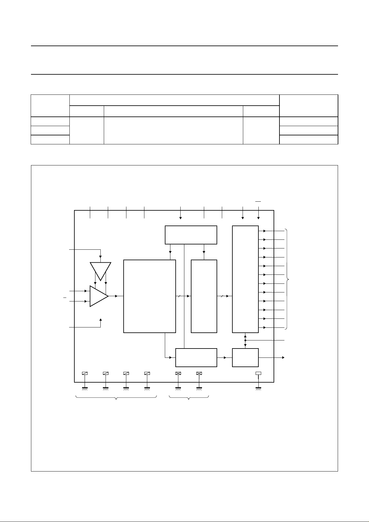
BLOCK DIAGRAM
V
V
V
handbook, full pagewidth
V
ref
V
V
SH
V
CCA1
CCA2
9
2
CCA3
CCA4
3
TDA8767
11
AMP
42
I
43
I
sample-
and-hold
39
ANALOG-TO-DIGITAL
CONVERTER
10
44
AGND1
10
AGND2
analog ground
4
AGND3
40
AGND4
38
DGND1
digital ground
Fig.1 Block diagram.
1999 Feb 16 3
IN-RANGE
LATCH
17
DGND2
CMOS
OUTPUT
OGND
20
34
IR
MBH142

Philips Semiconductors Preliminary specification
12-bit high-speed Analog-to-Digital
Converter (ADC)
PINNING
SYMBOL PIN DESCRIPTION
n.c. 1 not connected
V
CCA1
V
CCA3
AGND3 4 analog ground 3
n.c. 5 not connected
n.c. 6 not connected
n.c. 7 not connected
n.c. 8 not connected
V
CCA2
AGND2 10 analog ground 2
V
ref
n.c. 12 not connected
n.c. 13 not connected
n.c. 14 not connected
V
CCD2
n.c. 16 not connected
DGND2 17 digital ground 2
TC 18 output two’s complement
OE 19 output enable input
IR 20 in-range output
D11 21 data output; bit 11 (MSB)
D10 22 data output; bit 10
2 analog supply voltage 1 (+5 V)
3 analog supply voltage 3 (+5 V)
9 analog supply voltage 2 (+5 V)
11 reference voltage
15 digital supply voltage 2 (+5 V)
(CMOS level; active LOW)
TDA8767
SYMBOL PIN DESCRIPTION
D9 23 data output; bit 9
D8 24 data output; bit 8
D7 25 data output; bit 7
D6 26 data output; bit 6
D5 27 data output; bit 5
D4 28 data output; bit 4
D3 29 data output; bit 3
D2 30 data output; bit 2
D1 31 data output; bit 1
D0 32 data output; bit 0 (LSB)
V
CCO
OGND 34 output ground
n.c. 35 not connected
CLK 36 clock input
V
CCD1
DGND1 38 digital ground 1
SH 39 sample-and-hold enable input
AGND4 40 analog ground 4
V
CCA4
V
I
V
I
AGND1 44 analog ground 1
33 output supply voltage (3 to 5.25 V)
37 digital supply voltage 1 (+5 V)
(CMOS level; active HIGH)
41 analog supply voltage 4 (+5 V)
42 complementary analog input voltage
43 analog input voltage
1999 Feb 16 4

Philips Semiconductors Preliminary specification
12-bit high-speed Analog-to-Digital
Converter (ADC)
handbook, full pagewidth
IVI
V
43
42
n.c.
V
CCA1
V
CCA3
AGND3
n.c.
n.c.
n.c.
n.c.
V
CCA2
AGND2
V
ref
AGND1
44
1
2
3
4
5
6
7
8
9
10
11
CCA4
V
41
AGND4
SH
40
39
TDA8767
DGND1
V
38
37
CCD1
CLK
36
n.c.
35
OGND
34
TDA8767
V
33
CCO
D0
32
31
D1
30
D2
D3
29
28
D4
D5
27
26
D6
D7
25
24
D8
D9
23
12
n.c.
13
14
15
16
17
n.c.
n.c.
CCD2
V
n.c.
DGND2
Fig.2 Pin configuration.
18
TC
19
OE
20
21
IR
D11
22
D10
MBH143
1999 Feb 16 5
Philips Semiconductors Preliminary specification
12-bit high-speed Analog-to-Digital
TDA8767
Converter (ADC)
LIMITING VALUES
In accordance with the Absolute Maximum Rating System (IEC 134).
SYMBOL PARAMETER CONDITIONS MIN. MAX. UNIT
V
V
V
∆V
V
V
I
O
T
T
T
CCA
CCD
CCO
CC
I
i(p-p)
stg
amb
j
analog supply voltage note 1 −0.3 +7.0 V
digital supply voltage note 1 −0.3 +7.0 V
output supply voltage note 1 −0.3 +7.0 V
supply voltage difference
− V
V
V
V
CCA
CCO
CCA
− V
− V
CCD
CCD
CCO
input voltage referenced to AGND 0.3 V
input voltage for differential clock
−1.0 +1.0 V
−1.0 +4.0 V
−1.0 +4.0 V
CCA
− V
CCD
drive (peak-to-peak value)
output current − 10 mA
storage temperature −55 +150 °C
operating ambient temperature 0 70 °C
junction temperature − +150 °C
V
V
Note
1. The supply voltages V
CCA
, V
CCD
and V
may have any value between −0.3 V and +7.0 V provided that the supply
CCO
voltage differences ∆VCC are respected.
HANDLING
Inputs and outputs are protected against electrostatic discharges in normal handling. However, to be totally safe, it is
desirable to take normal precautions appropriate to handling integrated circuits.
THERMAL CHARACTERISTICS
SYMBOL PARAMETER VALUE (TYP.) UNIT
R
th j-a
thermal resistance from junction to ambient in free air 75 K/W
1999 Feb 16 6
 Loading...