

Philips TDA8761A Service Manual
INTEGRATED CIRCUITS
DATA SH EET
TDA8761A
9-bit analog-to-digital converter
for digital video
Preliminary specification
File under Integrated Circuits, IC02
1996 Feb 13
Philips Semiconductors Preliminary specification
9-bit analog-to-digital converter
for digital video
FEATURES
• 9-bit resolution
• Sampling rate up to 40 MHz
• DC sampling allowed
• One clock cycle conversion only
• High signal-to-noise ratio over a large analog input
frequency range (8.2 effective bits at 10 MHz full-scale
input at f
• No missing codes guaranteed
• In range (IR) CMOS output
• CMOS compatible digital inputs
• 3 to 5 V CMOS digital outputs
• Low-level AC clock input signal allowed
• External reference voltage regulator
• Power dissipation only 165 mW (typical)
• Low analog input capacitance, no buffer amplifier
required
• No sample-and-hold circuit required.
= 30 MHz)
clk
TDA8761A
APPLICATIONS
Analog-to-digital conversion for:
• Video data digitizing
• Digital Video Broadcasting (DVB)
• Cable TV.
GENERAL DESCRIPTION
The TDA8761A is a 9-bit analog-to-digital converter (ADC)
for professional video and digital video set box
applications. It converts the analog input signal into 9-bit
binary-coded digital words at a maximum sampling rate of
40 MHz. Its linearity performance ensures the required
conversion accuracy in the event of 256QAM demodulator
concept and for all symbol frequencies. All digital inputs
and outputs are CMOS compatible, although a low-level
sine wave clock input signal is allowed.
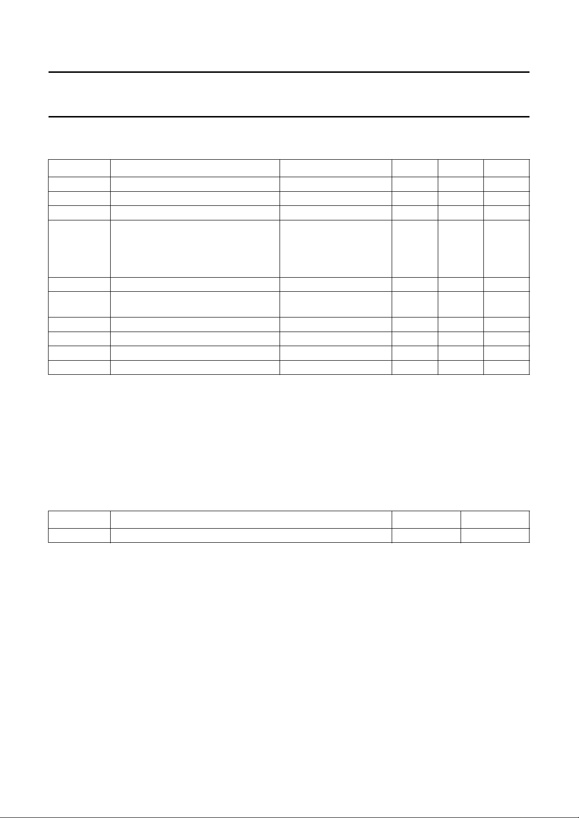
QUICK REFERENCE DATA
SYMBOL PARAMETER CONDITIONS MIN. TYP. MAX. UNIT
V
CCA
V
CCD
V
CCO
I
CCA
I
CCD
I
CCO
INL integral non-linearity f
analog supply voltage 4.75 5.0 5.25 V
digital supply voltage 4.75 5.0 5.25 V
output stages supply voltage 3.0 3.3 5.25 V
analog supply current − 18 tbf mA
digital supply current − 13 tbf mA
output stages supply current f
= 30 MHz; ramp input − 3 tbf mA
clk
= 30 MHz; ramp input −±0.8 tbf LSB
clk
AINL AC integral non-linearity full-scale input sine wave; note 1 −±0.75 tbf LSB
50% full-scale input sine wave; note 1 −±0.5 tbf LSB
DNL differential non-linearity f
= 30 MHz; ramp input −±0.3 ±0.7 LSB
clk
ADNL AC differential non-linearity full-scale input sine wave; note 1 −±0.5 tbf LSB
50% full-scale input sine wave; note 1 −±0.3 tbf LSB
f
clk(max)
P
tot
maximum clock frequency 40 −−MHz
total power dissipation − 165 tbf mW
Note
= 10 MHz and f
1. f
i
= 30 MHz; fi= 8 MHz and f
clk
= 20 MHz.
clk
1996 Feb 13 2
Philips Semiconductors Preliminary specification
9-bit analog-to-digital converter
TDA8761A
for digital video
ORDERING INFORMATION
TYPE
NUMBER
NAME DESCRIPTION VERSION
TDA8761AM SSOP28 plastic shrink small outline package; 28 leads; body width 5.3 mm SOT341-1
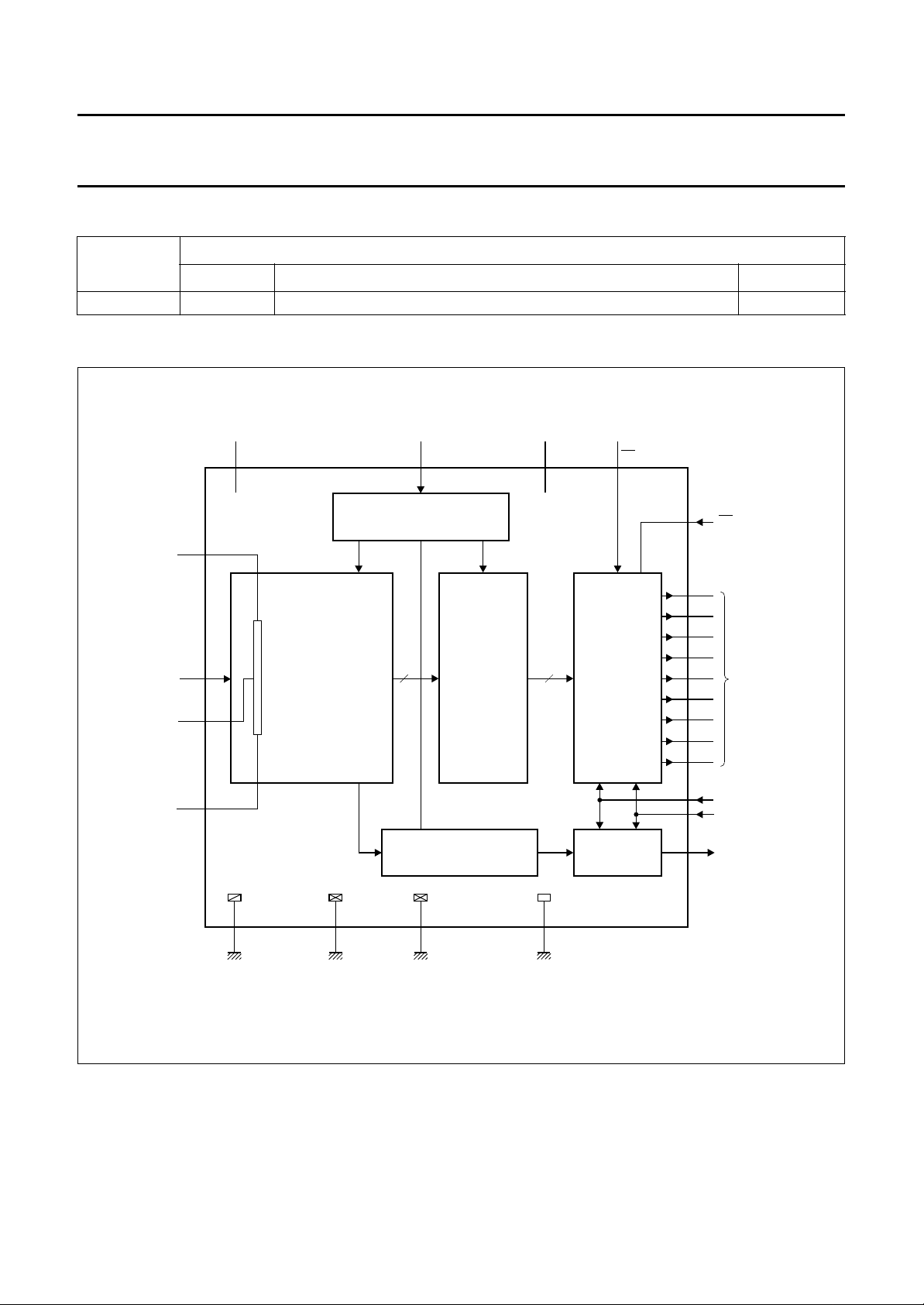
BLOCK DIAGRAM
handbook, full pagewidth
analog
voltage input
V
RT
V
V
RM
V
CCA
3
9
R
LAD
I
8
7
ANALOG -TO - DIGITAL
CONVERTER
CLK
1
CLOCK DRIVER
PACKAGE
LATCHES
V
CCD2
11
TDA8761A
OE
10
CMOS
OUTPUTS
2
25
D8
D7
24
D6
23
D5
22
D4
21
20 D3
19
D2
18
D1
17 D0
TC
MSB
data outputs
LSB
V
6
RB
IN RANGE LATCH
4
AGND
analog ground digital grounds
12
DGND2
27
DGND1
Fig.1 Block diagram.
1996 Feb 13 3
14
OGND
output ground
CMOS OUTPUT
13
28
26
MBG910
V
CCO
V
CCD1
IR
output
Philips Semiconductors Preliminary specification
9-bit analog-to-digital converter
for digital video
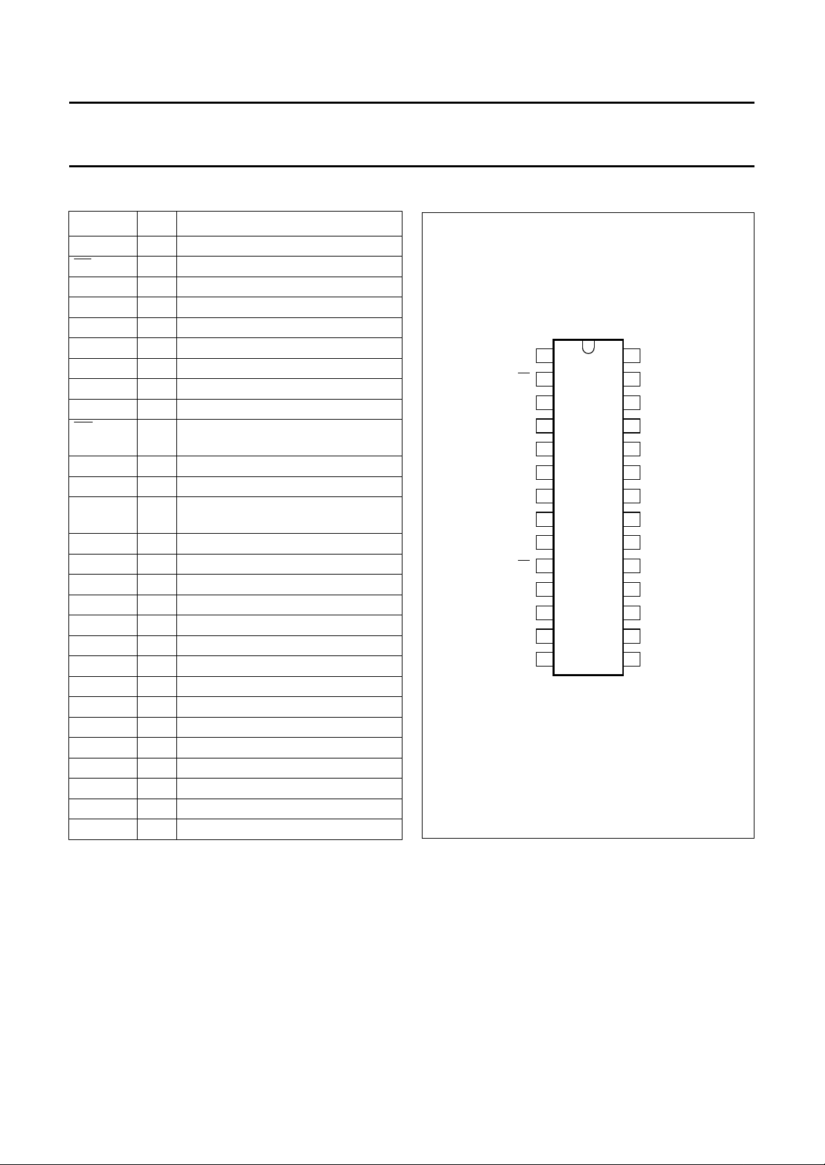
PINNING
SYMBOL PIN DESCRIPTION
CLK 1 clock input
TC 2 two’s complement input (active LOW)
V
CCA
AGND 4 analog ground
n.c. 5 not connected
V
RB
V
RM
V
I
V
RT
OE 10 output enable input (CMOS level
V
CCD2
DGND2 12 digital ground 2
V
CCO
OGND 14 output ground
n.c. 15 not connected
n.c. 16 not connected
D0 17 data output; bit 0 (LSB)
D1 18 data output; bit 1
D2 19 data output; bit 2
D3 20 data output; bit 3
D4 21 data output; bit 4
D5 22 data output; bit 5
D6 23 data output; bit 6
D7 24 data output; bit 7
D8 25 data output; bit 8 (MSB)
IR 26 in range data output
DGND1 27 digital ground 1
V
CCD1
3 analog supply voltage (+5 V)
6 reference voltage BOTTOM input
7 reference voltage MIDDLE
8 analog input voltage
9 reference voltage TOP input
input, active LOW)
11 digital supply voltage 2 (+5 V)
13 supply voltage for output stages
(+3 to 5 V)
28 digital supply voltage 1 (+5 V)
handbook, halfpage
1
CLK
2
TC
V
3
CCA
4
AGND
5
n.c.
V
6
RB
V
7
RM
V
RT
OE
V
CCD2
DGND2
V
CCO
OGND
V
I
TDA8761A
8
9
10
11
12
13
MBG909
Fig.2 Pin configuration.
TDA8761A
V
28
CCD1
27
DGND1
IR
26
25
D8
24
D7
23
D6
22
D5
D4
21
20
D3
D2
19
18
D1
17
D0
16
n.c.
1514
n.c.
1996 Feb 13 4
Philips Semiconductors Preliminary specification
9-bit analog-to-digital converter
TDA8761A
for digital video
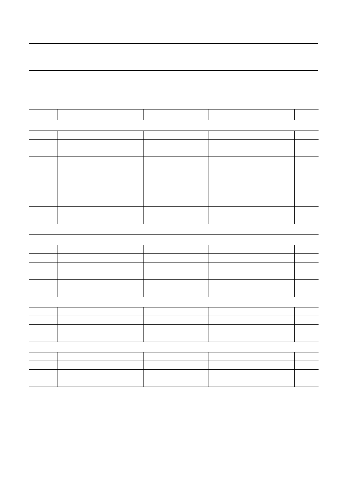
LIMITING VALUES
In accordance with the Absolute Maximum Rating System (IEC 134).
SYMBOL PARAMETER CONDITIONS MIN. MAX. UNIT
V
V
V
∆V
V
V
I
O
T
T
T
CCA
CCD
CCO
CC
I
i(p-p)
stg
amb
j
analog supply voltage note 1 −0.3 +7.0 V
digital supply voltage note 1 −0.3 +7.0 V
output stages supply voltage note 1 −0.3 +7.0 V
supply voltage differences between
V
V
V
CCA
CCD
CCA
and V
and V
and V
CCD
CCO
CCO
−1.0 +1.0 V
−1.0 +4.0 V
−1.0 +4.0 V
input voltage referenced to AGND −0.3 +7.0 V
AC input voltage for switching
referenced to DGND − V
CCD
(peak-to-peak value)
output current − 10 mA
storage temperature −55 +150 °C
operating ambient temperature 0 +70 °C
junction temperature − +150 °C
V
Note
1. The supply voltages V
CCA
, V
CCD
and V
may have any value between −0.3 and +7.0 V provided that the supply
CCO
voltage differences ∆VCC are respected.
HANDLING
Inputs and outputs are protected against electrostatic discharges in normal handling. However, to be totally safe, it is
desirable to take normal precautions appropriate to handling integrated circuits.
THERMAL CHARACTERISTICS
SYMBOL PARAMETER VALUE UNIT
R
th j-a
thermal resistance from junction to ambient in free air 110 K/W
1996 Feb 13 5
Philips Semiconductors Preliminary specification
9-bit analog-to-digital converter
TDA8761A
for digital video
CHARACTERISTICS
V
CCA=V3
AGND and DGND shorted together; T
V
CCO
SYMBOL PARAMETER CONDITIONS MIN. TYP. MAX. UNIT
Supply
V
CCA
V
CCD
V
CCO
∆V
I
CCA
I
CCD
I
CCO
Inputs
to V4= 4.75 to 5.25 V; V
= 3.3 V; V
i(p-p)
analog supply voltage 4.75 5.0 5.25 V
digital supply voltage 4.75 5.0 5.25 V
output stages supply voltage 3.0 3.3 5.25 V
CC
supply voltage differences
between
V
CCA
V
CCA
V
CCD
analog supply current − 18 tbf mA
digital supply current − 13 tbf mA
output stages supply current f
CCD=V11
= 0 to +70 °C; typical values measured at V
amb
= 1.8 V; CL= 15 pF and T
and V
CCD
and V
CCO
and V
CCO
to V12and V28to V27= 4.75 to 5.25 V; V
=25°C; unless otherwise specified.
amb
CCO=V13
CCA=VCCD
to V14= 3.0 to 5.25 V;
= 5 V and
−0.2 − +0.2 V
−0.2 − +2.25 V
−0.2 − +2.25 V
= 30 MHz; ramp input − 3 tbf mA
clk
LOCK INPUT CLK (REFERENCED TO DGND); note 1
C
V
IL
V
IH
I
IL
I
IH
Z
i
C
i
LOW level input voltage 0 − 0.3V
HIGH level input voltage 0.7V
LOW level input current V
HIGH level input current V
input impedance f
input capacitance f
= 0.3V
clk
= 0.7V
clk
=30MHz − 2 − kΩ
clk
=30MHz − 2 − pF
clk
INPUTS OE AND TC (REFERENCED TO DGND); see Table 2
V
IL
V
IH
I
IL
I
IH
V
(ANALOG INPUT VOLTAGE REFERENCED TO AGND)
I
I
IL
I
IH
Z
i
C
i
LOW level input voltage 0 − 0.3V
HIGH level input voltage 0.7V
LOW level input current VIL= 0.3V
HIGH level input current VIH= 0.7V
LOW level input current VI=VRB= 1.3 V − 0 −µA
HIGH level input current VI=VRT= 3.43 V − 35 −µA
input impedance fi= 10 MHz − 8 − kΩ
input capacitance fi= 10 MHz − 5 − pF
CCD
CCD
CCD
CCD
V
V
CCD
− V
CCD
CCD
−10+1 µA
− 210 µA
V
V
CCD
− V
CCD
CCD
−1 −− µA
−−1 µA
1996 Feb 13 6
 Loading...