

Philips SL1ICS3001U-L6D, SL1ICS3001U-N5D, SL1ICS3001W-N5D Datasheet

INTEGRATED CIRCUITS
SL1 ICS30 01
Philips
I•CODE1 Label IC
Chip Specification
Product Specification
Revision 2.1
Public
Semiconductors
2000-05-02

I•CODE1 Chip Specification Rev. 2.1 May 2000
1 Contents
1 CONTENTS 2
2 DEFINITIONS 4
2.1 Life Support Applications ....................................................................................................4
2.2 Abbreviations ........................................................................................................................4
3 SCOPE 5
4 ORDERING INFORMATION 5
5 FUNCTIONAL DESCRIPTION 6
5.1 Basic Features.......................................................................................................................6
5.2 Block Diagram of the IC.......................................................................................................6
5.3 Memory Organisation...........................................................................................................7
5.3.1 Serial Number...................................................................................................................7
5.3.2 Write Access Conditions ..................................................................................................7
5.3.3 Special Functions (EAS/QUIET) .....................................................................................8
5.3.4 Family Code and Application Identifier ...........................................................................8
5.3.5 Configuration of delivered ICs.........................................................................................8
6 MECHANICAL DIE SPECIFICATIONS 9
7 MECHANICAL WAFER SPECIFICATIONS 10
7.1 Wafer Status ........................................................................................................................10
7.2 Backside Treatment ............................................................................................................10
8 DOCUMENTATION 11
8.1 Delivery Documentation.....................................................................................................11
8.2 Fail-Die Identification.........................................................................................................11
8.2.1 Ink Dot Specification......................................................................................................11
8.2.2 Wafer Mapping...............................................................................................................11
9 QUALITY ASSURANCE 12
9.1 Electrical Acceptance Test.................................................................................................12
9.2 Visual Inspection.................................................................................................................12
9.2.1 After Wafer Final Test....................................................................................................12
9.2.2 After Sawing (Film Frame Carrier)................................................................................12
10 PACKING 13
10.1 Storage Recommendations.................................................................................................13
10.2 Possible Forms of Delivery.................................................................................................13
10.2.1 Packing of Unsawn Wafers............................................................................................13
10.2.2 Packing of Sawn Wafers................................................................................................13
SL040521.doc/M Public Page 2 of 22

I•CODE1 Chip Specification Rev. 2.1 May 2000
11 HANDLING RECOMMENDATIONS 14
11.1 Sawing ..................................................................................................................................14
11.2 Die Attach.............................................................................................................................14
11.3 Wire Bonding.......................................................................................................................14
12 COIL SPECIFICATION 14
13 ELECTRICAL SPECIFICATIONS 15
14 HINTS FOR LABEL IC ENCAPSULATION 16
14.1 Protection against Visible Light.........................................................................................16
14.2 Protection against UV Light...............................................................................................16
14.3 Resistance to X-Rays ..........................................................................................................16
15 INLET/LABEL CHARA CTERISATION AND TEST 17
15.1 Characterisation of the Inlet/Label...................................................................................17
15.2 Final Test of the Inlet/Label...............................................................................................17
16 APPENDIX A: DIE PLAN 18
17 APPENDIX B: CLUS TER PLAN 19
18 APPENDIX C: CLUS TER MAP 20
19 APPENDIX D: WAFER MAP 21
SL040521.doc/M Public Page 3 of 22

I•CODE1 Chip Specification Rev. 2.1 May 2000
2 Definitions
Data sheet status
Objective specification This data sheet contains target or goal specifications for product development.
Preliminary specification This data sheet contains preliminary data; supplementary data may be published later.
Product specification This data sheet contains final product specifications.
Limiting values
Limiting values given are in accordance with the Absolute Maximum Rating System (IEC 134). Stress above one
or more of the limiting values may cause permanent damage to the device. These are stress ratings only and
operation of the device at these or at any other conditions above those given in the Characteristics section of the
specification is not implied. Exposure to limiting values for extended periods may affect device reliability.
Application information
Where application information is given, it is advisory and does not form part of the specification.
2.1 Life Support Applications
These products are not designed for use in life support appliances, devices, or systems where
malfunction of these products can reasonably be expected to result in personal injury. Philips
customers using or selling these products for use in such applications do so on their own risk and
agree to fully indemnify Philips for any damages resulting from such improper use or sale.
2.2 Abbreviations
ASCII American Standard Code for Information Interchange
CSC Cyclic Redundancy Check
EAN European Article Number
EAS Electronic Article Surveillance
EEPROM Electrically Erasable and Programmable Read Only Memory
EMI Electromagnetic Interference
ETSI European Telecommunications Standards Institute
FCC Federal Communications Commission
FFC Film Frame Carrier
Hex Value in hexadecimal notation
IC Integrated Circuit
ISM Industrial, Scientific, Medical
LSB Least Significant Bit or Byte
MSB Most Significant Bit or Byte
MTBF Mean Time Between Failure
PCB Printed Circuit Board
PCM Process Control Module
RF Radio Frequency
rms Root Mean Square
SNR Serial Number
UV Ultraviolet
SL040521.doc/M Public Page 4 of 22

I•CODE1 Chip Specification Rev. 2.1 May 2000
3 Scope
This specification describes the electrical, physical and dimensional properties of unsawn and sawn
wafers on FFC of I•CODE1 Label ICs on a Philips 6C15 IDFW process and is the base for delivery
of tested I•CODE1 Label ICs.
General recommendations are given for storage, handling and processing of wafers as well as
assembly of labels.
Reference documents: MIL-STD 883D Method 3023
MIL-STD 883D Method 3015
SNW-FQ-627
PICTOH-QS007
General Specification for 6” Wafer (Prod. Spec.)
General Quality Specification
I•CODE1 Label IC, Coil Design Guide
This product specification is valid for VCOL1V0 from mask revision P/B upwards.
4 Ordering Information
Following ordering options are available:
Type Name Description Ordering Code
SL1 ICS30 01W/N5D Sawn wafer on foil (FFC), 150 µm, inked and mapped 9352 644 66005
SL1 ICS30 01U/N5D Unsawn wafer, 150 µm, inked and mapped 9352 644 65025
SL1 ICS30 01U/L6D
Unsawn wafer, 525 µm, mapped (not inked)
9352 644 64025
SL040521.doc/M Public Page 5 of 22

I•CODE1 Chip Specification Rev. 2.1 May 2000
5 Functional Description
5.1 Basic Features
The I•CODE1 Label IC is a dedicated chip for intelligent label applications like logistics and retail
(including EAS) as well as baggage and parcel identification in airline business and mail services.
The I•CODE system offers the possibility of operating labels simultaneously in the field of the
reader antenna (Anticollision). It is designed for long range applications.
Whenever connected to a very simple and cheap type of antenna (as a result of the 13.56 MHz
carrier frequency) made out of a few windings printed, winded, etched or punched coil the
I•CODE1 Label IC can be operated without line of sight up to a distance of 1.5 m (gate width).
5.2 Block Diagram of the IC
The label requires no internal power supply. Its contactless interface generates the power supply
and the system clock via the resonant circuitry by inductive coupling to the reader. The interface
also demodulates data that are transmitted from the reader to the I•CODE Label, and modulates the
electromagnetic field for data transmission from the I•CODE Label to the reader.
Data are stored in a non-volatile memory (EEPROM). The EEPROM has a memory capacity of 512
bit and is organised in 16 blocks consisting of 4 bytes each (1 block = 32 bits). The higher 12 blocks
contain user data and the lowest 4 blocks contain the serial number, the write access conditions and
some configuration bits.
SL040521.doc/M Public Page 6 of 22
I•CODE1 Chip Specification Rev. 2.1 May 2000
â
MSB LSB
â
â
MSB LSB
â
â
MSB LSB
â
â
MSB LSB
â
1|1
1|1
0|0
0|0
1|1
1|1
1|1
1|1
1|1
1|1
1|1
1|1
1|1
1|1
1|1
1|1
Funct.
Access
Data
.....
.....
.....
.....
.....
.....
.....
.....
.....
.....
Data
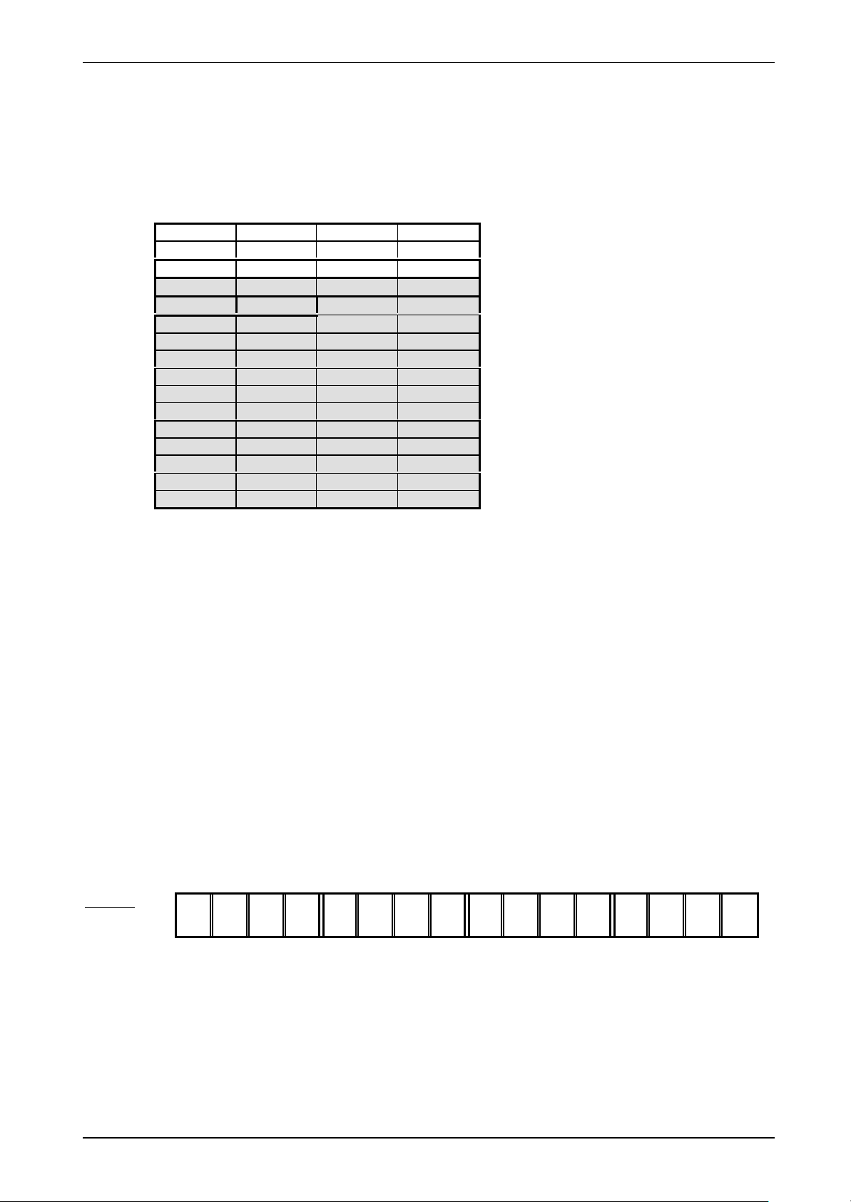
5.3 Memory Organisation
The 512 bit EEPROM memory is divided into 16 blocks. A block is the smallest access unit. Each
block consists of 4 bytes (1 block = 32 bits). Bit 0 in each byte represents the least significant bit
(LSB) and bit 7 the most significant bit (MSB), respectively.
Byte 0 Byte 1 Byte 2 Byte 3
Block 0 SNR0 SNR1 SNR2 SNR3 Serial Number (lower bytes)
Block 1 SNR4 SNR5 SNR6 SNR7 Serial Number (higher bytes)
Block 2 F0 FF FF FF Write Access Conditions
Block 3 x x x x Special Functions (EAS/QUIET)
Block 4 x x x x Family Code/Application Identifier/User Data
Block 5 x x x x User Data
Block 6 x x x x :
Block 7 x x x x :
Block 8 x x x x :
Block 9 x x x x :
Block 10 x x x x :
Block 11 x x x x :
Block 12 x x x x :
Block 13 x x x x :
Block 14 x x x x :
Block 15 x x x x User Data
The values (in hexadecimal notation) shown in the table above are stored in the EEPROM after the
wafer production process. The contents of blocks marked with ‘x’ in the table are not defined at
delivery.
5.3.1 Serial Number
The unique 64 bit serial number is stored in blocks 0 and 1 and is programmed during the
production process. SNR0 in the table represents the least significant byte and SNR7 the most
significant byte, respectively.
5.3.2 Write Access Conditions
The Write Access Condition bits in block 2 determine the write access conditions for each of the
16 blocks. These bits can be set only to 0 (and never be changed to 1), i.e. already write protected
blocks can never be written to from this moment on. This is also true for block 2. If this block is set
into write protected state by clearing of bits 4 and 5 at byte 0, no further changes in write access
conditions are possible.
Byte 0 Byte 1 Byte 2 Byte 3
Block 2:
Write Access
Conditions
for Block à
|
|
|
|
|
|
|
|
|
|
|
|
|
|
|
|
|
|
|
|
|
|
|
|
|
|
|
|
3 2 1 0 7 6 5 4 11 10 9 8 15 14 13 12
Special
Write
Serial
Number
User
|
|
|
|
User
The ones in the 16 pairs of bits have to be cleared together if the corresponding block is wanted to
be write protected forever (1|1 à write access enabled, 0|0 à write access disabled). Writing of bit
pairs 1|0 or 0|1 to block 2 is not allowed!
It is extremely important to be particularly careful when clearing the Write Access bits in
block 2, as you can lose write access to all of the blocks on the label in case of a mistake.
Of course you can use this feature to put the label into a hardware write protected state!
SL040521.doc/M Public Page 7 of 22
 Loading...