

Philips pcf8583 DATASHEETS

INTEGRATED CIRCUITS
DATA SH EET
PCF8583
Clock Calendar with 256 x 8-bit
Static RAM
Product specification
File under Integrated Circuits, IC01
October 1991
Philips Semiconductors Product specification
Clock Calendar with 256 x 8-bit Static
RAM
FEATURES
• I2C-bus interface operating supply voltage: 2.5 V to 6 V
• Clock operating supply voltage (0 to +70 °C):
1.0 V to 6.0 V
• Data retention voltage: 1.0 V to 6 V
• Operating current (f
• Clock function with four year calendar
• Universal timer with alarm and overflow indication
• 24 or 12 hour format
• 32.768 kHz or 50 Hz time base
• Serial input/output bus (I2C)
• Automatic word address incrementing
• Programmable alarm, timer and interrupt function
• Slave address,
READ: A1 or A3,
WRITE: A0 or A2.
= 0 Hz): max. 50 A
scl
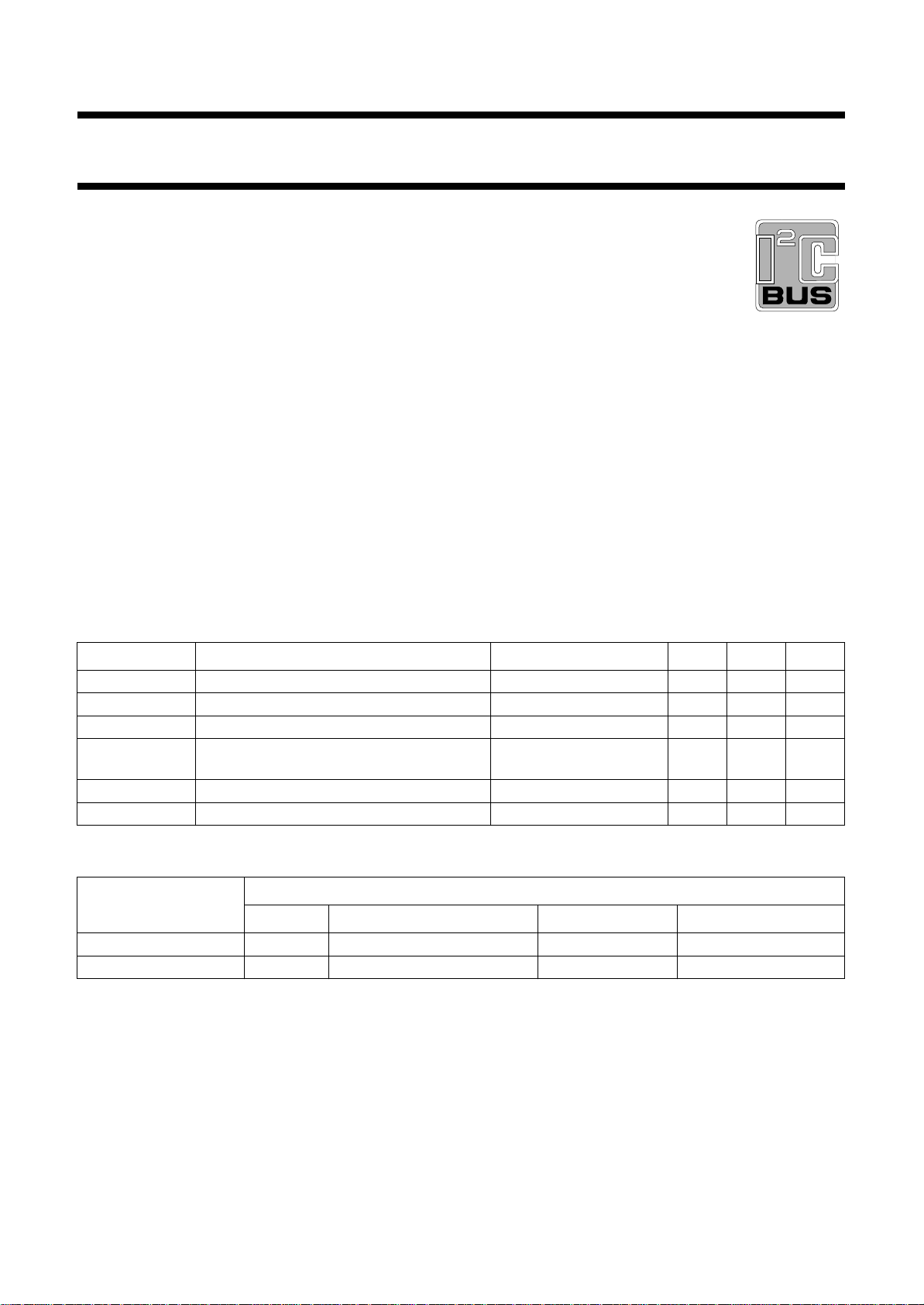
PCF8583
GENERAL DESCRIPTION
The PCF8583 is a low power 2048-bit static CMOS RAM
organized as 256 words by 8 bits. Addresses and data are
transferred serially via a two-line bidirectional bus (I2C).
The built-in word address register is incremented
automatically after each written or read data byte. One
address pin A0 is used for programming the hardware
address, allowing the connection of two devices to the bus
without additional hardware. The built-in 32.768 kHz
oscillator circuit and the first 8 bytes of the RAM are used
for the clock/calendar and counter functions. The next
8 bytes may be programmed as alarm registers or used as
free RAM space.
QUICK REFERENCE DATA
SYMBOL PARAMETER CONDITION MIN. MAX. UNIT
V
V
I
DD
I
DDO
T
T
DD
DD
amb
stg
supply voltage operating range I2C-bus active 2.5 6.0 V
supply voltage operating range I2C-bus inactive 1.0 6.0 V
supply current operating mode f
supply current clock mode f
= 100 kHz − 200 µA
scl
= 0 Hz; VDD = 5 V
scl
f
= 0 Hz; VDD = 1 V
scl
−
−
50
10
operating ambient temperature range −40 +85 °C
storage temperature range −65 +150 °C
ORDERING INFORMATION
EXTENDED PACKAGE
TYPE NUMBER PINS PIN POSITION MATERIAL CODE
PCF8583P
PCF8583T
(1)
(2)
8 DIL plastic SOT97
8 mini-pack plastic SO8L; SOT176C
Notes
1. SOT97-1; 1996 August 19.
2. SOT176-1; 1996 August 19.
µA
µA
October 1991 2
Philips Semiconductors Product specification
Clock Calendar with 256 x 8-bit Static RAM PCF8583
handbook, full pagewidth
OSCI
OSCO
INT
V
DD
V
SS
A0
SCL
SDA
1
2
7
8
4
3
6
5
PCF8583
OSCILLATOR
32.768 kHz
POWER-ON
RESET
2
C-BUS
I
INTERFACE
DIVIDER
1 : 256
OR
100 : 128
CONTROL
LOGIC
ADDRESS
REGISTER
100 Hz
control/status
hundredth of a second
seconds
minutes
hours
year/date
weekdays/months
timer
alarm control
alarm registers
of RAM
RAM
(256 × 8)
00
01
07
08
0F
FF
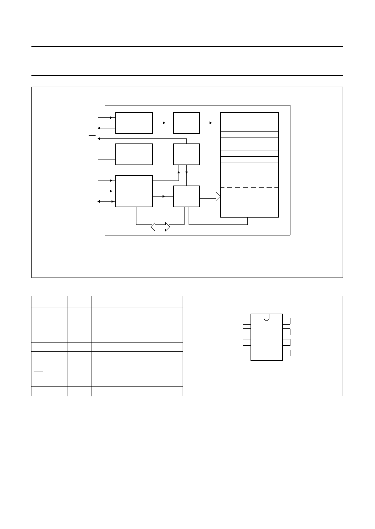
PINNING
SYMBOL PIN DESCRIPTION
OSCI 1 oscillator input, 50 Hz or
event-pulse input
OSCO 2 oscillator output
A0 3 address input
V
SS
4 negative supply
SDA 5 serial data line
SCL 6 serial clock line
INT 7 open drain interrupt output
(active LOW)
V
DD
8 positive supply
Fig.1 Block diagram.
1
OSCI
2
OSCO
V
SS
A0
PCF8583P
PCF8583T
3
4
MRB014
Fig.2 Pinning diagram.
MRB001
V
8
DD
7
INT
6
SCL
5
SDA
October 1991 3

Philips Semiconductors Product specification
Clock Calendar with 256 x 8-bit Static RAM PCF8583
FUNCTIONAL DESCRIPTION
The PCF8583 contains a 256 by 8-bit RAM with an 8-bit
auto-increment address register, an on-chip 32.768 kHz
oscillator circuit, a frequency divider, a serial two-line
bidirectional I2C-bus interface and a power-on reset circuit.
The first 8 bytes of the RAM (memory addresses 00 to 07)
are designed as addressable 8-bit parallel registers. The
first register (memory address 00) is used as a
control/status register. The memory addresses 01 to 07
are used as counters for the clock function. The memory
addresses 08 to 0F are free RAM locations or may be
programmed as alarm registers.
Counter function modes
When the control/status register is programmed, a 32.768
kHz clock mode, a 50 Hz clock mode or an event-counter
mode can be selected.
In the clock modes the hundredth of a second, seconds,
minutes, hours, date, month (four year calendar) and
weekday are stored in a BCD format. The timer register
stores up to 99 days. The event counter mode is used to
count pulses applied to the oscillator input (OSCO left
open). The event counter stores up to 6 digits of data.
When one of the counters is read (memory locations 01 to
07), the contents of all counters are strobed into capture
latches at the beginning of a read cycle. Therefore, faulty
reading of the count during a carry condition is prevented.
When a counter is written, other counters are not affected.
Alarm function modes
By setting the alarm enable bit of the control/status register
the alarm control register (address 08) is activated.
By setting the alarm control register a dated alarm, a daily
alarm, a weekday alarm or a timer alarm may be
programmed. In the clock modes, the timer register
(address 07) may be programmed to count hundredths of
a second, seconds, minutes, hours or days. Days are
counted when an alarm is not programmed.
Whenever an alarm event occurs the alarm flag of the
control/status register is set. A timer alarm event will set
the alarm flag and an overflow condition of the timer will set
the timer flag. The open drain interrupt output is switched
on (active LOW) when the alarm or timer flag is set
(enabled). The flags remain set until directly reset by a
write operation.
When a timer function without any function is programmed
the remaining alarm registers (addresses 09 to 0F) may be
used as free RAM space.
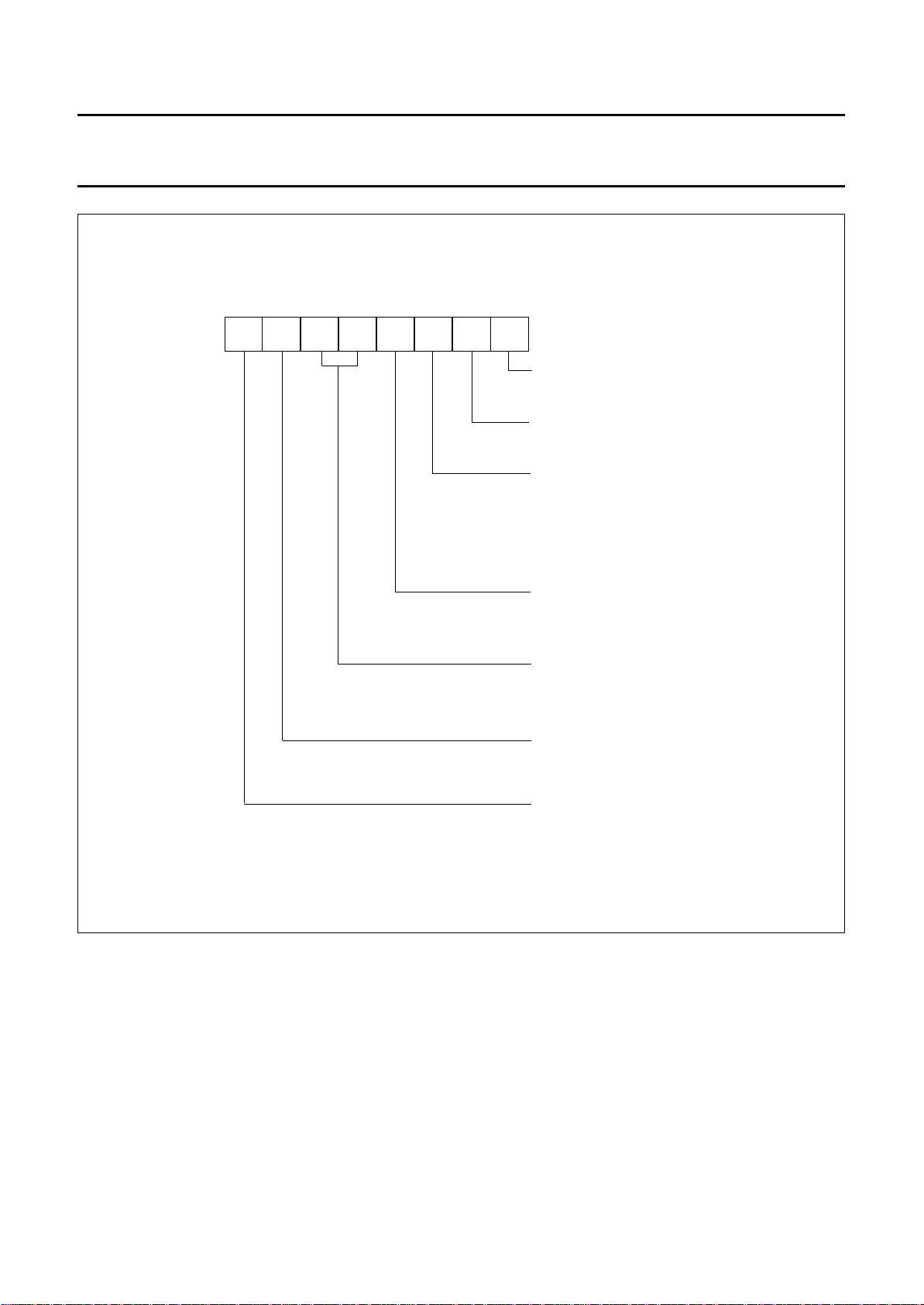
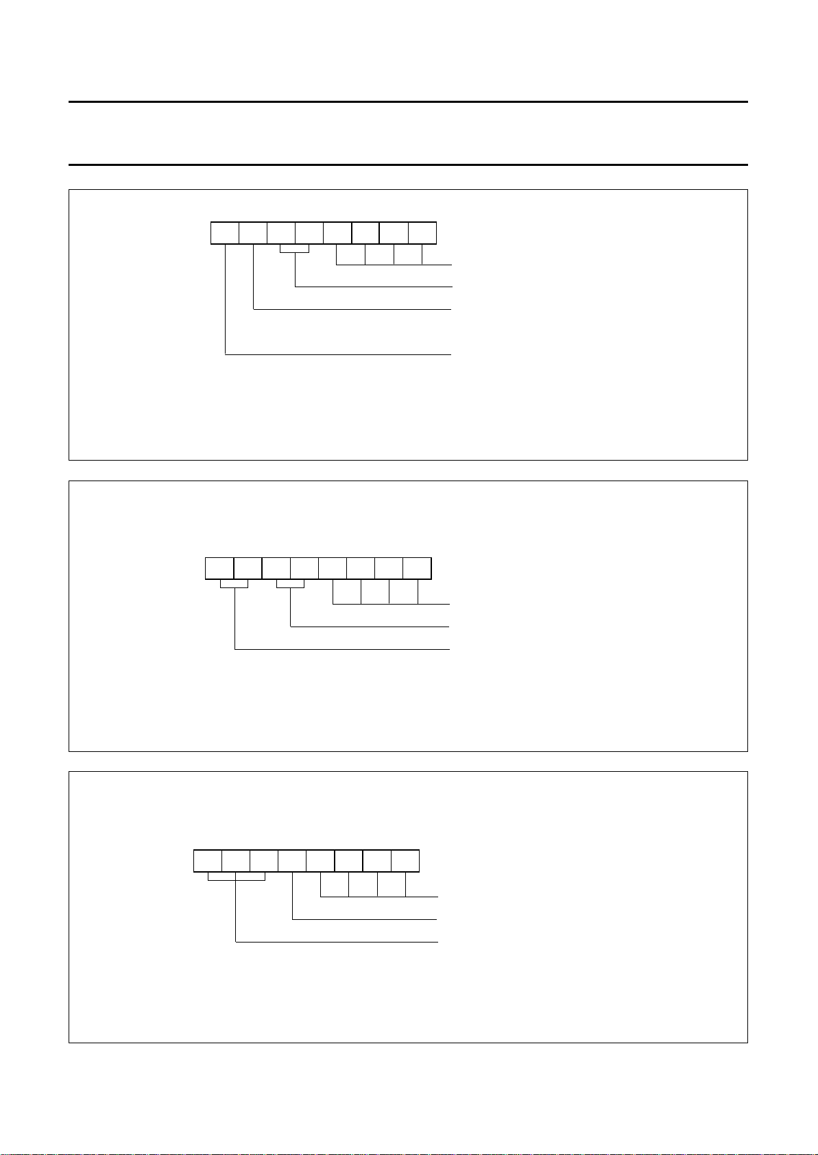
Control/status register
The control/status register is defined as the memory
location 00 with free access for reading and writing via the
2
C-bus. All functions and options are controlled by the
I
contents of the control/status register (see Fig.3).
Counter registers
In the clock modes 24 h or 12 h format can be selected by
setting the most significant bit of the hours counter
register. The format of the hours counter is shown in Fig.5.
The year and date are packed into memory location 05
(see Fig.6). The weekdays and months are packed into
memory location 06 (see Fig.7). When reading these
memory locations the year and weekdays are masked out
when the mask flag of the control/status register is set.
This allows the user to read the date and month count
directly.
In the event-counter mode events are stored in BCD
format. D5 is the most significant and D0 the least
significant digit. The divider is by-passed.
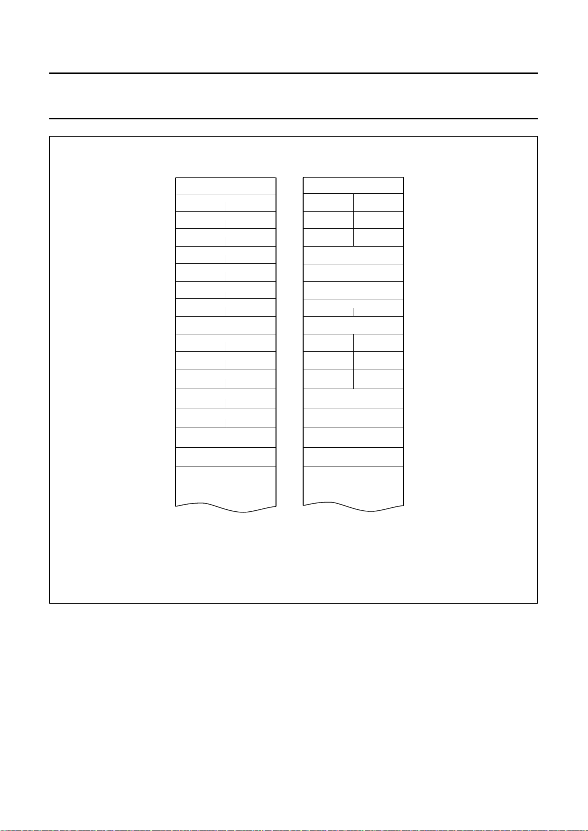
In the different modes the counter registers are
programmed and arranged as shown in Fig.4. Counter
cycles are listed in Table 1.
October 1991 4
Philips Semiconductors Product specification
Clock Calendar with 256 x 8-bit Static RAM PCF8583
handbook, full pagewidth
MSB LSB
76543210
MRB017
memory location 00
reset state: 0000 0000
timer flag (50% duty factor
seconds flag if alarm
enable bit is 0)
alarm flag (50% duty factor
minutes flag if alarm
enable bit is 0)
alarm enable bit:
0 alarm disabled: flags toggle
alarm control register disabled
(memory locations 08 to 0F
are free RAM space)
1 enable alarm control register
(memory location 08 is the
alarm control register)
mask flag:
0 read locations 05 to 06
unmasked
1 read date and month count
directly
function mode :
00 clock mode 32.768 kHz
01 clock mode 50 Hz
10 event-counter mode
11 test modes
hold last count flag :
0 count
1 store and hold last count in
capture latches
stop counting flag :
0 count pulses
1 stop counting, reset divider
October 1991 5
Fig.3 Control/status register.
Philips Semiconductors Product specification
Clock Calendar with 256 x 8-bit Static RAM PCF8583
handbook, full pagewidth
control/status
hundredth of a second
1/10 s
10 s
10 min
10 h
10 day
weekday/month
10 month
10 day
alarm control
hundredth of a second
1/10 s 1/100 s
alarm seconds
alarm minutes
alarm hours
alarm month
alarm timer
1/100 s
seconds
1 s
minutes
1 min
hours
1 h
year/date
1 day
1 month
timer
1 day
alarm date
control/status
D1
D3
D5
T1
alarm control
alarm alarm
D1
D3
D5
alarm timer
free
free
free
timer
free
free
free
D0
D2
D4
T0
D0
D2
D4
00
01
02
03
04
05
06
07
08
09
0A
0B
0C
0D
0E
0F
free RAM free RAM
CLOCK MODES EVENT COUNTER
Fig.4 Register arrangement.
October 1991 6
MRB015
Philips Semiconductors Product specification
Clock Calendar with 256 x 8-bit Static RAM PCF8583
handbook, full pagewidth
handbook, full pagewidth
MSB LSB
76543210
MRB002
Fig.5 Format of the hours counter.
MSB LSB
765 43210
MRB003
memory location 04 (hours counter)
reset state: 0000 0000
unit hours BCD
ten hours (0 to 2 binary)
AM/PM flag:
0 AM
1 PM
format:
0 24 h format, AM/PM flag
remains unchanged
1 12 h format, AM/PM flag
will be updated
memory location 05 (year/date)
reset state: 0000 0001
unit hours BCD
ten days (0 to 3 binary)
year (0 to 3 binary, read as 0 if
the mask flag is set)
Fig.6 Format of the year/date counter.
handbook, full pagewidth
MSB LSB
76543 210
MRB004
Fig.7 Format of the weekdays/months counter.
October 1991 7
memory location 06 (weekdays/months)
reset state: 0000 0001
unit months BCD
ten months
weekdays (0 to 6 binary, read as 0 if
the mask flag is set)
Philips Semiconductors Product specification
Clock Calendar with 256 x 8-bit Static RAM PCF8583
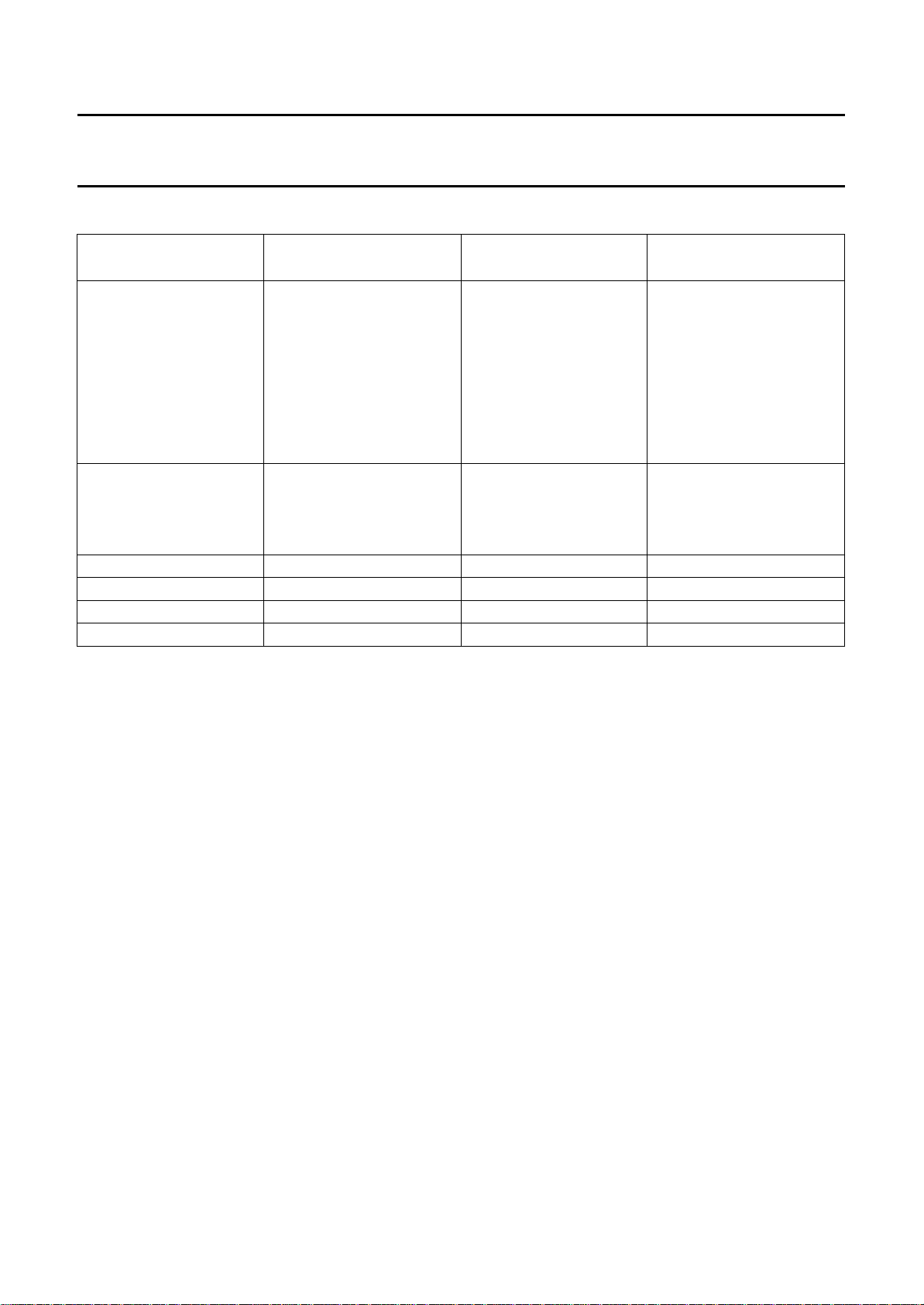
Table 1 Cycle length of the time counters, clock modes
UNIT COUNTING CYCLE CARRY TO NEXT UNIT
hundredths of a second 00 to 99 99 to 00
seconds 00 to 59 59 to 00
minutes 00 to 59 59 to 00
hours (24 h) 00 to 23 23 to 00
hours (12 h) 12 AM;
01 AM to 11 AM;
12 PM;
01 PM to 11 PM 11 PM to 12 AM
date 01 to 31 31 to 01 1, 3, 5, 7, 8, 10, 12
01 to 30 30 to 01 4, 6, 9, 11
01 to 29 29 to 01 2, year = 0
01 to 28 28 to 01 2, year = 1, 2, 3
months 01 to 12 12 to 01
year 0 to 3
weekdays 0 to 6 6 to 0
timer 00 to 99 no carry
CONTENTS OF THE
MONTH COUNTER
October 1991 8
 Loading...