

Philips PCF8576CT Datasheet
INTEGRATED CIRCUITS
DATA SH EET
PCF8576C
Universal LCD driver for low
multiplex rates
Product specification
Supersedes data of 1997 Nov 14
File under Integrated Circuits, IC12
1998 Jul 30

Philips Semiconductors Product specification
Universal LCD driver for low multiplex
rates
CONTENTS
1 FEATURES
2 GENERAL DESCRIPTION
3 ORDERING INFORMATION
4 BLOCK DIAGRAM
5 PINNING
6 FUNCTIONAL DESCRIPTION
6.1 Power-on reset
6.2 LCD bias generator
6.3 LCD voltage selector
6.4 LCD drive mode waveforms
6.4.1 Static drive mode
6.4.2 1 : 2 multiplex drive mode
6.4.3 1 : 3 multiplex drive mode
6.4.4 1 : 4 multiplex drive mode
6.5 Oscillator
6.5.1 Internal clock
6.5.2 External clock
6.6 Timing
6.7 Display latch
6.8 Shift register
6.9 Segment outputs
6.10 Backplane outputs
6.11 Display RAM
6.12 Data pointer
6.13 Subaddress counter
6.14 Output bank selector
6.15 Input bank selector
6.16 Blinker
7 CHARACTERISTICS OF THE I2C-BUS
7.1 Bit transfer (see Fig.12)
7.2 Start and stop conditions (see Fig.13)
7.3 System configuration (see Fig.14)
7.4 Acknowledge (see Fig.15)
7.5 PCF8576C I2C-bus controller
7.6 Input filters
7.7 I2C-bus protocol
7.8 Command decoder
7.9 Display controller
7.10 Cascaded operation
PCF8576C
8 LIMITING VALUES
9 HANDLING
10 DC CHARACTERISTICS
11 AC CHARACTERISTICS
11.1 Typical supply current characteristics
11.2 Typical characteristics of LC D outputs
12 APPLICATION INFORMATION
12.1 Chip-on-glass cascadability in single plane
13 BONDING PAD LOCATIONS
14 PACKAGE OUTLINES
15 SOLDERING
15.1 Introduction
15.2 Reflow soldering
15.3 Wave soldering
15.3.1 LQFP
15.3.2 VSO
15.3.3 Method (LQFP and VSO)
15.4 Repairing soldered joints
16 DEFINITIONS
17 LIFE SUPPORT APPLICATIONS
18 PURCHASE OF PHILIPS I2C COMPONENTS
1998 Jul 30 2
Philips Semiconductors Product specification
Universal LCD driver for low multiplex
rates
1 FEATURES
• Single-chip LCD controller/driver
• Selectable backplane drive configuration: static or 2/3/4
backplane multiplexing
• Selectable display bias configuration: static, 1/2 or 1/3
• Internal LCD bias generation with voltage-follower
buffers
• 40 segment drives: up to twenty 8-segment numeric
characters; up to ten 15-segment alphanumeric
characters; or any graphics of up to 160 elements
• 40 × 4-bit RAM for display data storage
• Auto-incremented display data loading across device
subaddress boundaries
• Display memory bank switching in static and duplex
drive modes
• Versatile blinking modes
• LCD and logic supplies may be separated
• Wide power supply range: from 2 V for low-threshold
LCDs and up to 6 V for guest-host LCDs and
high-threshold (automobile) twisted nematic LCDs.
A 9 V version is also available on request.
• Low power consumption
• Power-saving mode for extremely low power
consumption in battery-operated and telephone
applications
2
C-bus interface
• I
• TTL/CMOS compatible
• Compatible with any 4-bit, 8-bit or 16-bit
microprocessors/microcontrollers
PCF8576C
• May be cascaded for large LCD applications (up to
2560 segments possible)
• Cascadable with 24-segment LCD driver PCF8566
• Optimized pinning for plane wiring in both and multiple
PCF8576C applications
• Space-saving 56-lead plastic very small outline package
(VSO56) or 64-lead low profile quad flat package
(LQFP64)
• No external components
• Compatible with chip-on-glass technology
• Manufactured in silicon gate CMOS process.
2 GENERAL DESCRIPTION
The PCF8576C is a peripheral device which interfaces to
almost any Liquid Crystal Display (LCD) with low multiplex
rates. It generates the drive signals for any static or
multiplexed LCD containing up to four backplanes and up
to 40 segments and can easily be cascaded for larger LCD
applications. The PCF8576C is compatible with most
microprocessors/microcontrollers and communicates via a
two-line bidirectional I2C-bus. Communication overheads
are minimized by a display RAM with auto-incremented
addressing, by hardware subaddressing and by display
memory switching (static and duplex drive modes).
3 ORDERING INFORMATION
TYPE NUMBER
NAME DESCRIPTION VERSION
PCF8576CT VSO56 plastic very small outline package; 56 leads SOT190-1
PCF8576CU − chip in tray −
PCF8576CU/2 − chip with bumps in tray −
PCF8576CU/5 − unsawn wafer −
PCF8576CU/7 − chip with bumps on tape −
PCF8576CU/10 FFC chip-on-film frame carrier −
PCF8576CU/12 FFC chip with bumps on film frame carrier −
PCF8576CH LQFP64 plastic low profile quad flat package; 64 leads; body 10 × 10 × 1.4 mm SOT314-2
1998 Jul 30 3
PACKAGE
This text is here in white to force landscape pages to be rotated correctly when browsing through the pdf in the Acrobat reader.This text is here in
_white to force landscape pages to be rotated correctly when browsing through the pdf in the Acrobat reader.This text is here inThis text is here in
white to force landscape pages to be rotated correctly when browsing through the pdf in the Acrobat reader. white to force landscape pages to be ...
1998 Jul 30 4
4 BLOCK DIAGRAM
Universal LCD driver for low multiplex
rates
Philips Semiconductors Product specification
V
DD
V
LCD
CLK
SYNC
OSC
V
SS
SCL
SDA
5
LCD BIAS
12
4
3
6
11
2
1
GENERATOR
TIMING BLINKER
OSCILLATOR
INPUT
FILTERS
VOLTAGE
SELECTOR
POWER-
ON
RESET
2
I C - BUS
CONTROLLER
LCD
10
BP014BP215BP116BP3
13
BACKPLANE
OUTPUTS
PCF8576C
DISPLAY
CONTROLLER
COMMAND
DECODER
INPUT
BANK
SELECTOR
S0 to S39
40
17 to 56
DISPLAY SEGMENT OUTPUTS
DISPLAY LATCH
SHIFT REGISTER
DISPLAY
RAM
40 x 4 BITS
DATA
POINTER
OUTPUT
BANK
SELECTOR
SUBADDRESS
COUNTER
9
SA0
Fig.1 Block diagram; VSO56.
handbook, full pagewidth
A07A18A2
MLD332
PCF8576C
Philips Semiconductors Product specification
Universal LCD driver for low multiplex
PCF8576C
rates
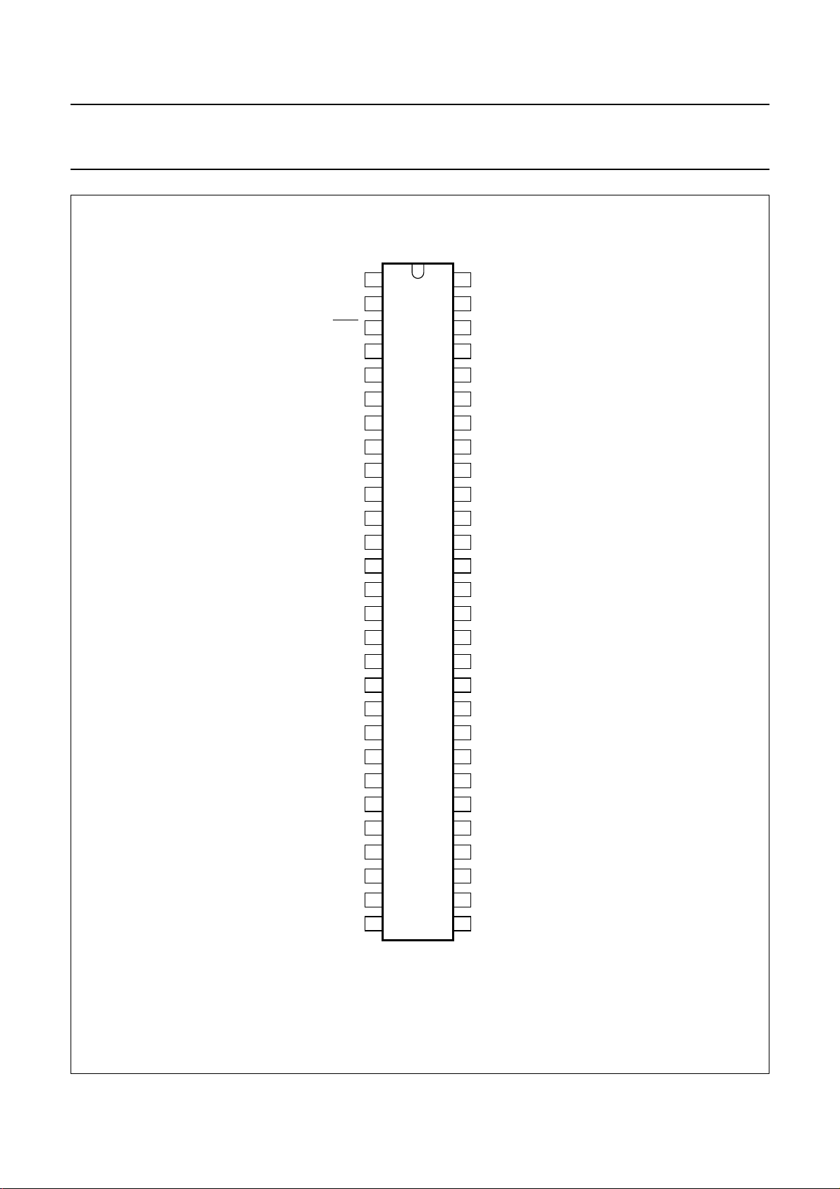
5 PINNING
SYMBOL
SOT190 SOT314
SDA 1 10 I
SCL 2 11 I
SYNC 3 12 cascade synchronization input/output
CLK 4 13 external clock input
V
DD
5 14 supply voltage
OSC 6 15 oscillator input
A0 to A2 7 to 9 16 to 18 I
SA0 10 19 I
V
V
SS
LCD
11 20 logic ground
12 21 LCD supply voltage
BP0, BP2, BP1, BP3 13 to 16 25 to 28 LCD backplane outputs
S0 to S39 17 to 56 29 to 32, 34 to 47, 49 to 64, 2 to 7 LCD segment outputs
n.c. − 1, 8, 9, 22 to 24, 33 and 48 not connected
PIN
DESCRIPTION
2
C-bus serial data input/output
2
C-bus serial clock input
2
C-bus subaddress inputs
2
C-bus slave address input; bit 0
1998 Jul 30 5
Philips Semiconductors Product specification
Universal LCD driver for low multiplex
rates
handbook, halfpage
SDA
SCL
SYNC
CLK
V
DD
OSC
A0
A1
A2
SA0
V
SS
V
LCD
BP0
BP2
BP1
BP3
S0
S1
S2
S3
S4
S5
S6
S7
S8
S9
S10
S11
1
2
3
4
5
6
7
8
9
10
11
12
13
14
PCF8576CT
15
16
17
18
19
20
21
22
23
24
25
26
27
28
MLD334
PCF8576C
56
S39
55
S38
54
S37
53
S36
52
S35
51
S34
50
S33
49
S32
48
S31
47
S30
46
S29
45
S28
44
S27
43
S26
42
S25
41
S24
40
S23
39
S22
38
S21
37
S20
36
S19
35
S18
34
S17
33
S16
32
S15
31
S14
30
S13
29
S12
Fig.2 Pin configuration; VSO56.
1998 Jul 30 6
Philips Semiconductors Product specification
Universal LCD driver for low multiplex
rates
handbook, full pagewidth
n.c.
S34
S35
S36
S37
S38
S39
n.c.
n.c.
SDA
SCL
SYNC
CLK
V
DD
OSC
A0
S33
S32
S31
S30
S29
S28
64
63
62
61
60
59
1
2
3
4
5
6
7
8
9
10
11
12
13
14
15
16
S27
S26
S25
58
57
56
PCF8576CH
S24
55
S23
54
S22
53
S21
52
S20
51
S19
50
S18
49
PCF8576C
48
n.c.
47
S17
46
S16
45
S15
44
S14
43
S13
42
S12
41
S11
40
S10
39
S9
38
S8
37
S7
36
S6
35
S5
34
S4
33
n.c.
17
18
19
20
21
22
23
A1
A2
SA0
SS
V
LCD
V
n.c.
n.c.
Fig.3 Pin configuration; LQFP64.
1998 Jul 30 7
24
n.c.
25
BP0
26
BP2
27
BP1
28
BP3
29
S0
30
S1
31
S2
32
S3
MLD333
Philips Semiconductors Product specification
Universal LCD driver for low multiplex
rates
6 FUNCTIONAL DESCRIPTION
The PCF8576C is a versatile peripheral device designed
to interface to any microprocessor/microcontroller to a
wide variety of LCDs. It can directly drive any static or
multiplexed LCD containing up to four backplanes and up
to 40 segments. The display configurations possible with
the PCF8576C depend on the number of active backplane
outputs required; a selection of display configurations is
given in Table 1.
All of the display configurations given in Table 1 can be
implemented in the typical system shown in Fig.4.
Table 1 Selection of display configurations
NUMBER OF 7-SEGMENTS NUMERIC
BACKPLANES SEGMENTS DIGITS
4 160 20 20 10 20 160 dots (4 × 40)
3 120 15 15 8 8 120 dots (3 × 40)
2 80 10 10 5 10 80 dots (2 × 40)
1 40 5 5 2 12 40 dots (1 × 40)
INDICATOR
SYMBOLS
PCF8576C
The host microprocessor/microcontroller maintains the
2
2-line I
PCF8576C. The internal oscillator is selected by tying
OSC (pin 6) to VSS (pin 11). The appropriate biasing
voltages for the multiplexed LCD waveforms are
generated internally. The only other connections required
to complete the system are to the power supplies (VDD,
VSS and V
application.
C-bus communication channel with the
) and the LCD panel chosen for the
LCD
14-SEGMENTS
ALPHANUMERIC
CHARACTERS
INDICATOR
SYMBOLS
DOT MATRIX
handbook, full pagewidth
V
DD
HOST
MICRO-
PROCESSOR/
MICRO-
CONTROLLER
V
SS
t
r
R
2C
B
SDA
SCL
OSC
V
DD
512
1 17 to 56
PCF8576CT
2
6
78
A0 A1 A2SSSA0 V
Fig.4 Typical system configuration.
1998 Jul 30 8
V
LCD
13 to 16
91011
40 segment drives
4 backplanes
LCD PANEL
(up to 160
elements)
MBE524
Philips Semiconductors Product specification
Universal LCD driver for low multiplex
rates
6.1 Power-on reset
At power-on the PCF8576C resets to a starting condition
as follows:
1. All backplane outputs are set to VDD.
2. All segment outputs are set to VDD.
3. The drive mode ‘1 : 4 multiplex with1⁄3bias’ is selected.
4. Blinking is switched off.
5. Input and output bank selectors are reset (as defined
in Table 5).
6. The I2C-bus interface is initialized.
7. The data pointer and the subaddress counter are
cleared.
2
Data transfers on the I
following power-on to allow completion of the reset action.
6.2 LCD bias generator
The full-scale LCD voltage (V
VDD− V
. The LCD voltage may be temperature
LCD
compensated externally through the V
Fractional LCD biasing voltages are obtained from an
internal voltage divider of the three series resistors
connected between VDD and V
be switched out of the circuit to provide a1⁄2bias voltage
level for the 1 : 2 multiplex configuration.
C-bus should be avoided for 1 ms
) is obtained from
op
supply to pin 12.
LCD
. The centre resistor can
LCD
PCF8576C
6.3 LCD voltage selector
The LCD voltage selector co-ordinates the multiplexing of
the LCD in accordance with the selected LCD drive
configuration. The operation of the voltage selector is
controlled by MODE SET commands from the command
decoder. The biasing configurations that apply to the
preferred modes of operation, together with the biasing
− V
characteristics as functions of V
op=VDD
resulting discrimination ratios (D), are given in Table 2.
A practical value for Vop is determined by equating V
with a defined LCD threshold voltage (Vth), typically when
the LCD exhibits approximately 10% contrast. In the static
drive mode a suitable choice is Vop>3Vth approximately.
Multiplex drive ratios of 1 : 3 and 1 : 4 with
possible but the discrimination and hence the contrast
ratios are smaller ( = 1.732 for 1 : 3 multiplex or
21
= 1.528 for 1 : 4 multiplex).
---------3
3
The advantage of these modes is a reduction of the LCD
full-scale voltage V
• 1 : 3 multiplex (
Vop= = 2.449 V
6V
×
as follows:
op
1
⁄2bias):
off rms〈〉
off(rms)
• 1 : 4 multiplex (1⁄2bias):
and the
LCD
1
⁄2bias are
off(rms)
These compare with Vop=3V
Table 2 Preferred LCD drive modes: summary of characteristics
LCD DRIVE MODE
NUMBER OF
BACKPLANES LEVELS
LCD BIAS
CONFIGURATION
static 1 2 static 0 1 ∞
1:2 2 3
1:2 2 4
1:3 3 4
1:4 4 4
V
43×()
= = 2.309 V
op
----------------------- 3
V
-------------------- -
1
⁄
2
1
⁄
3
1
⁄
3
1
⁄
3
off(rms)
when1⁄3bias is used.
off(rms)
off(rms)
V
op
V
on(rms)
-------------------- V
op
D
V
=
-------------------- V
on(rms)
off(rms)
0.354 0.791 2.236
0.333 0.745 2.236
0.333 0.638 1.915
0.333 0.577 1.732
1998 Jul 30 9
Philips Semiconductors Product specification
Universal LCD driver for low multiplex
PCF8576C
rates
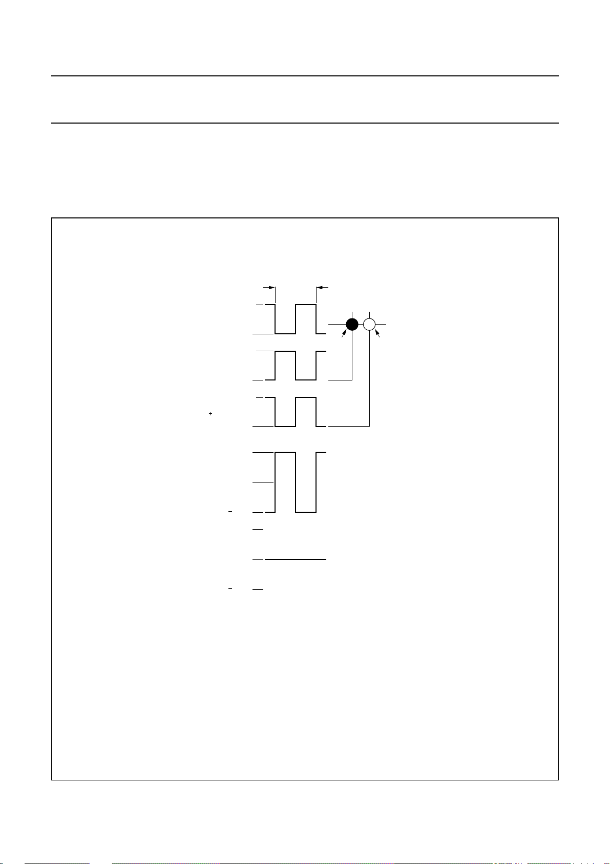
6.4 LCD drive mode waveforms
6.4.1 S
The static LCD drive mode is used when a single backplane is provided in the LCD. Backplane and segment drive
waveforms for this mode are shown in Fig.5.
TATIC DRIVE MODE
S
BP0
S
n 1
T
frame
V
DD
V
LCD
V
DD
n
V
LCD
V
DD
V
LCD
(a) waveforms at driver
V
op
LCD segments
state 1
(on)
state 2
(off)
V
t() V
state1
=
V
on(rms)Vop
V
t() V
state2
V
off(rms)
state 1 0
V
op
V
op
state 2 0
V
op
(b) resultant waveforms
at LCD segment
t() V
t() V
BP0
BP0
t()–=
t()–=
S
n
S
n1+
0V=
Fig.5 Static drive mode waveforms (Vop=VDD− V
MBE539
LCD
).
1998 Jul 30 10
Philips Semiconductors Product specification
Universal LCD driver for low multiplex
PCF8576C
rates
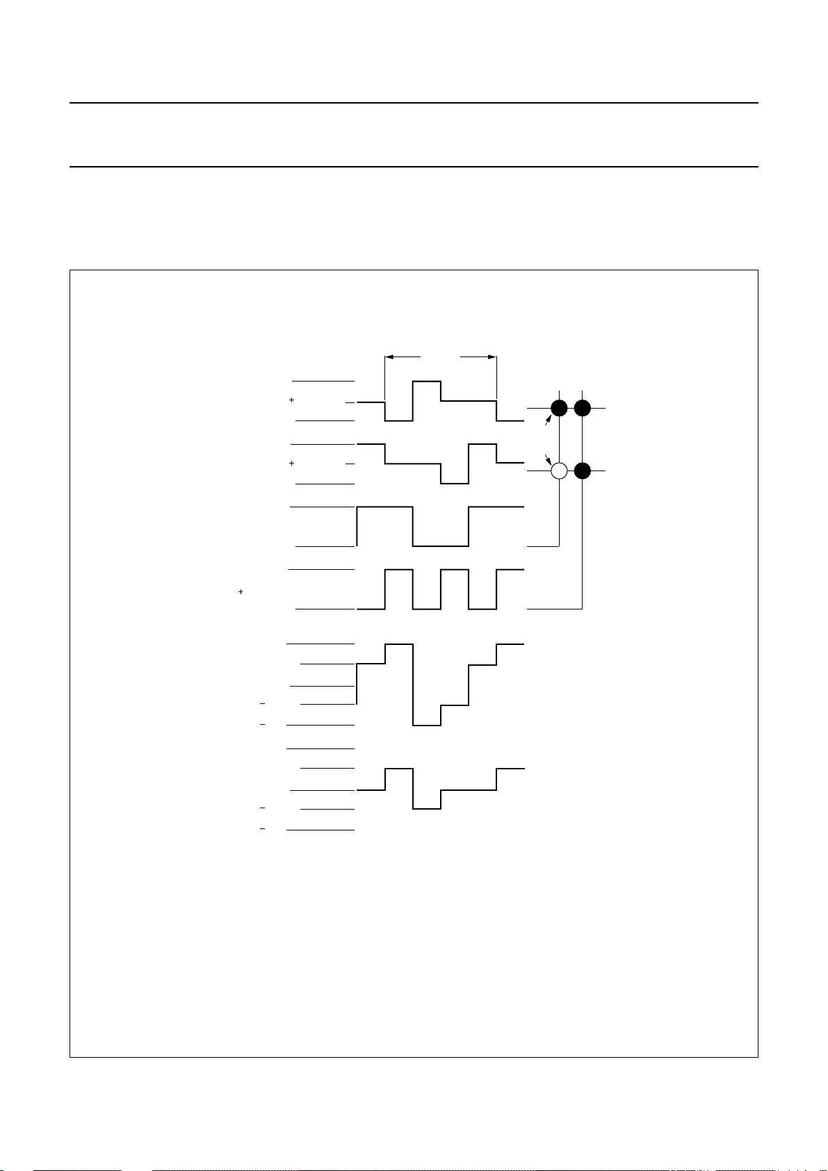
6.4.2 1 : 2 MULTIPLEX DRIVE MODE
When two backplanes are provided in the LCD, the 1 : 2 multiplex mode applies. The PCF8576C allows use of1⁄2bias or
1
⁄3bias in this mode as shown in Figs 6 and 7.
T
frame
V
(V )/2V
BP0
V
V
(V )/2V
BP1
V
V
S
n
V
V
S
n 1
V
V
V /2
state 1 0
V /2
V
V
V /2
state 2
V /2
V
DD
DD LCD
LCD
DD
LCD
DD
LCD
DD
LCD
DD
LCD
op
op
op
op
op
op
0
op
op
(a) waveforms at driver
(b) resultant waveforms
at LCD segment
LCD segments
state 1
state 2
MBE540
V
t() V
t() V
op
t() V
op
BP0
BP1
t()–=
t()–=
state1
V
on(rms)
V
state2
V
off(rms)
0.791V
=
t() V
0.354V
=
S
n
S
n
Fig.6 Waveforms for the 1 : 2 multiplex drive mode with1⁄2bias (Vop=VDD− V
1998 Jul 30 11
LCD
).
Philips Semiconductors Product specification
Universal LCD driver for low multiplex
rates
V
DD
V V /3
op
BP0
BP1
S
n
S
n 1
state 1 0
state 2 0
DD
V 2V /3
V
V
V V /3
V 2V /3
V
V
V V /3
V 2V /3
V
V
V V /3
V 2V /3
V
DD
LCD
DD
DD
DD
LCD
DD
DD
DD
LCD
DD
DD
DD
LCD
V
op
2V /3
op
V /3
op
V /3
op
2V /3
op
V
op
V
op
2V /3
op
V /3
op
V /3
op
2V /3
op
V
op
op
op
op
op
op
op
op
(a) waveforms at driver
(b) resultant waveforms
T
frame
at LCD segment
PCF8576C
LCD segments
state 1
state 2
MBE541
V
t() V
t() V
op
t() V
op
BP0
BP1
t()–=
t()–=
state1
V
on(rms)
V
state2
V
off(rms)
0.745V
=
t() V
0.333V
=
S
n
S
n
Fig.7 Waveforms for the 1 : 2 multiplex drive mode with1⁄3bias (Vop=VDD− V
1998 Jul 30 12
LCD
).
Philips Semiconductors Product specification
Universal LCD driver for low multiplex
PCF8576C
rates
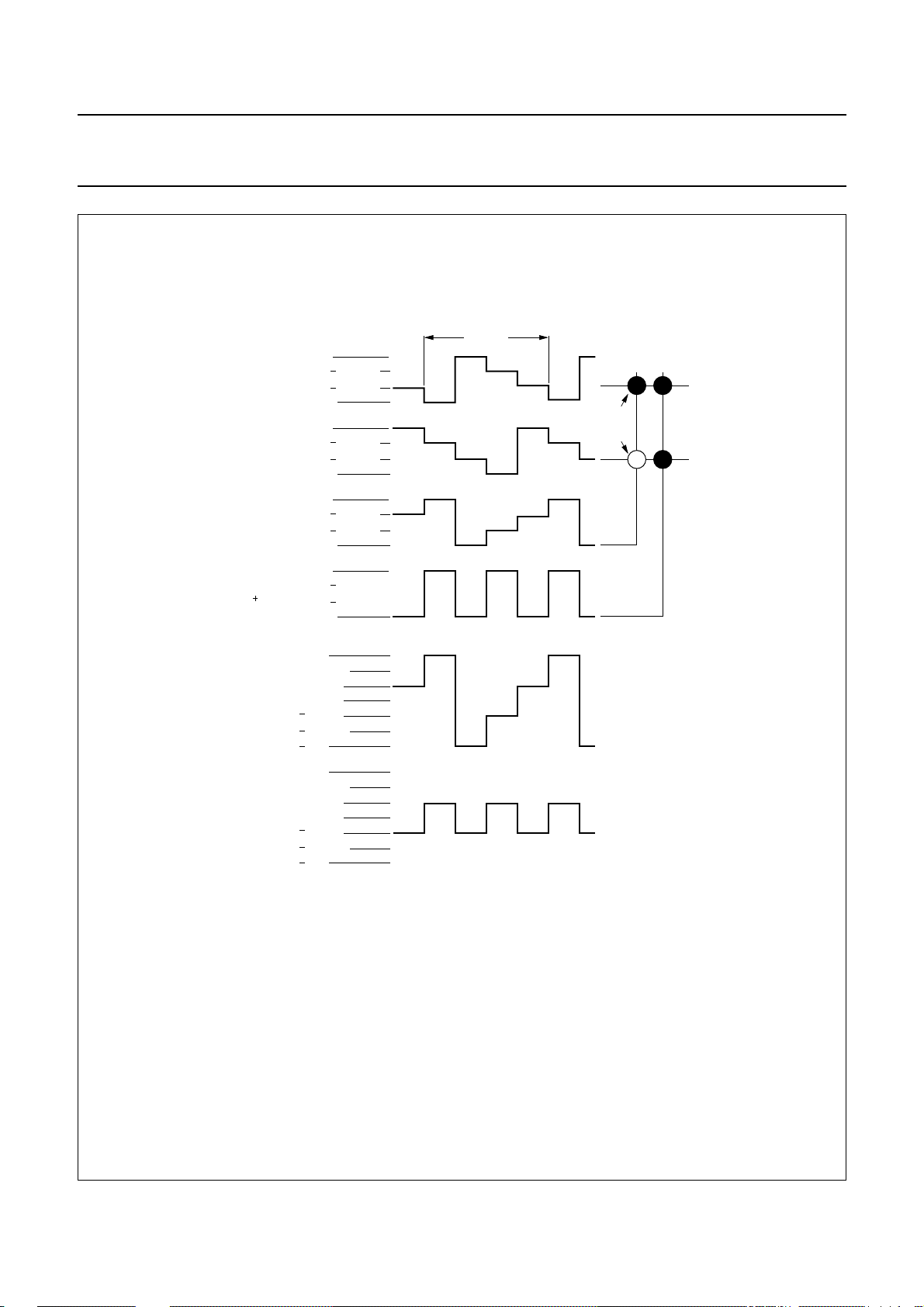
6.4.3 1 : 3 MULTIPLEX DRIVE MODE
When three backplanes are provided in the LCD, the 1 : 3 multiplex drive mode applies, as shown in Fig.8.
T
frame
(a) waveforms at driver
(b) resultant waveforms
at LCD segment
LCD segments
state 1
state 2
MBE542
V
state1
V
on(rms)
V
state2
V
off(rms)
t() V
0.638V
=
t() V
0.333V
=
S
S
t() V
n
t() V
n
BP0
BP1
BP2/S23
S
S
n 1
S
n 2
state 1 0
state 2 0
t()–=
BP0
op
t()–=
BP1
op
n
V
DD
V V /3
op
DD
V 2V /3
V
V
V V /3
V 2V /3
V
V
V V /3
V 2V /3
V
V
V V /3
V 2V /3
V
V
V V /3
V 2V /3
V
V
V V /3
V 2V /3
V
V
V
V
V
DD
LCD
DD
DD
DD
LCD
DD
DD
DD
LCD
DD
DD
DD
LCD
DD
DD
DD
LCD
DD
DD
DD
LCD
op
2V /3
op
V /3
op
V /3
op
2V /3
op
op
op
2V /3
op
V /3
op
V /3
op
2V /3
op
op
op
op
op
op
op
op
op
op
op
op
op
Fig.8 Waveforms for the 1 : 3 multiplex drive mode (Vop=VDD− V
1998 Jul 30 13
LCD
).
Philips Semiconductors Product specification
Universal LCD driver for low multiplex
PCF8576C
rates
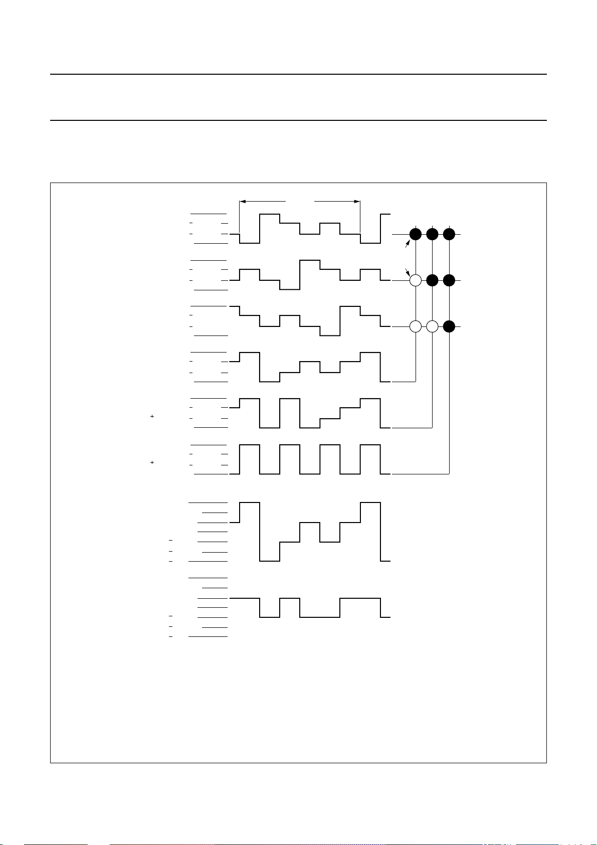
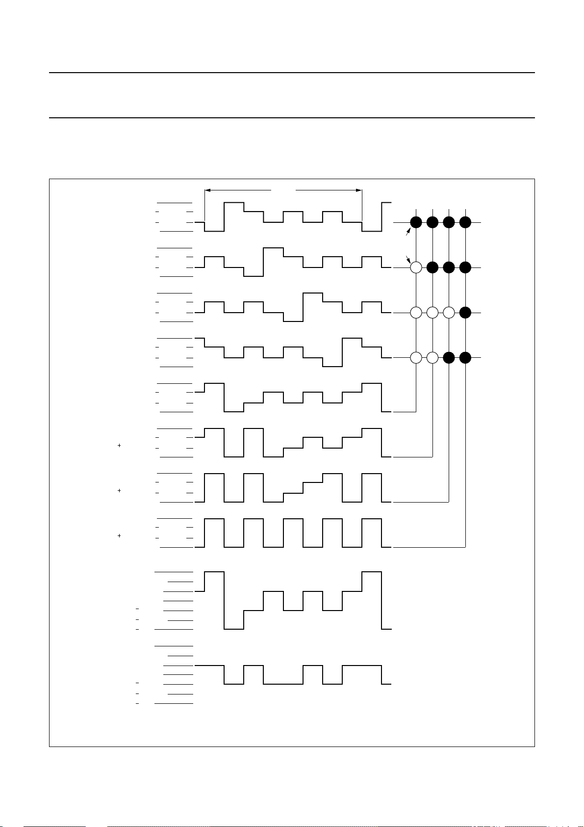
6.4.4 1 : 4 MULTIPLEX DRIVE MODE
When four backplanes are provided in the LCD, the 1 : 4 multiplex drive mode applies, as shown in Fig.9.
T
V
DD
V V /3
n
DD
V 2V /3
DD
V
LCD
V
DD
V V /3
DD
V 2V /3
DD
V
LCD
V
DD
V V /3
DD
V 2V /3
DD
V
LCD
V
DD
V V /3
DD
V 2V /3
DD
V
LCD
V
DD
V V /3
DD
V 2V /3
DD
V
LCD
V
DD
V V /3
DD
V 2V /3
DD
V
LCD
V
DD
V V /3
DD
V 2V /3
DD
V
LCD
V
DD
V V /3
DD
V 2V /3
DD
V
LCD
V
op
2V /3
op
V /3
op
V /3
op
2V /3
op
V
op
V
op
2V /3
op
V /3
op
V /3
op
2V /3
op
V
op
BP0
BP1
BP2
BP3
S
S
n 1
S
n 2
S
n 3
state 1 0
state 2 0
Fig.9 Waveforms for the 1 : 4 multiplex drive mode (Vop=VDD− V
op
op
op
op
op
op
op
op
op
op
op
op
op
op
op
op
frame
(a) waveforms at driver
(b) resultant waveforms
at LCD segment
state 1
state 2
LCD segments
V
state1
V
on(rms)
V
state2
V
off(rms)
MBE543
LCD
).
t() V
0.577V
=
t() V
0.333V
=
S
n
S
n
t() V
op
t() V
op
BP0
BP1
t()–=
t()–=
1998 Jul 30 14
 Loading...