

Philips PCF8573U-5-F3, PCF8573P, PCF8573T, PCF8573U-5-F1 Datasheet
DATA SH EET
Product specification
Supersedes data of May 1989
File under Integrated Circuits, IC12
1997 Mar 28
INTEGRATED CIRCUITS
PCF8573
Clock/calendar with Power Fail
Detector

1997 Mar 28 2
Philips Semiconductors Product specification
Clock/calendar with Power Fail Detector PCF8573
CONTENTS
FEATURES
2 GENERAL DESCRIPTION
3 QUICK REFERENCE DATA
4 ORDERING INFORMATION
5 BLOCK DIAGRAM
6 PINNING
7 FUNCTIONAL DESCRIPTION
7.1 Oscillator
7.2 Prescaler and time counter
7.3 Alarm register
7.4 Comparator
7.5 Power on/power fail detection
7.6 Interface level shifters
8 CHARACTERISTICS OF THE I2C-BUS
8.1 Bit transfer
8.2 Start and stop conditions
8.3 System configuration
8.4 Acknowledge
9I
2
C-BUS PROTOCOL
9.1 Addressing
9.2 Clock/calendar READ/WRITE cycles
10 LIMITING VALUES
11 HANDLING
12 DC CHARACTERISTICS
13 AC CHARACTERISTICS
14 APPLICATION INFORMATION
15 PACKAGE OUTLINES
16 SOLDERING
16.1 Introduction
16.2 DIP
16.2.1 Soldering by dipping or by wave
16.2.2 Repairing soldered joints
16.3 SO
16.3.1 Reflow soldering
16.3.2 Wave soldering
16.3.3 Repairing soldered joints
17 DEFINITIONS
18 LIFE SUPPORT APPLICATIONS
19 PURCHASE OF PHILIPS I2C COMPONENTS
1997 Mar 28 3
Philips Semiconductors Product specification
Clock/calendar with Power Fail Detector PCF8573
1 FEATURES
• Serial input/output I2C-bus interface for minutes, hours,
days and months
• Additional pulse outputs for seconds and minutes
• Alarm register for presetting a time for alarm or remote
switching functions
• On-chip power fail detector
• Separate ground pin for the clock allows easy
implementation of battery back-up during supply
interruption
• Crystal oscillator control (32.768 kHz)
• Low power consumption.
2 GENERAL DESCRIPTION
The PCF8573 is a low threshold, CMOS circuit that
functions as a real time clock/calendar. Addresses and
data are transferred serially via the two-line bidirectional
I2C-bus.
The IC incorporates an addressable time counter and an
addressable alarm register for minutes, hours, days and
months. Three special control/status flags, COMP, POWF
and NODA, are also available. Back-up for the clock during
supply interruptions is provided by a 1.2 V nickel cadmium
battery. The time base is generated from a 32.768 kHz
crystal-controlled oscillator.
3 QUICK REFERENCE DATA
4 ORDERING INFORMATION
SYMBOL PARAMETER MIN. TYP. MAX. UNIT
V
DD
− V
SS1
supply voltage, clock (pin 16 to pin 15) 1.1 − 6.0 V
V
DD
− V
SS2
supply voltage, I2C-bus (pin 16 to pin 8) 2.5 − 6.0 V
f
osc
crystal oscillator frequency − 32.768 − kHz
TYPE NUMBER
PACKAGE
NAME DESCRIPTION VERSION
PCF8573P DIP16 plastic dual in-line package; 16 leads (300 mil); long body SOT38-1
PCF8573T SO16 plastic small outline package; 16 leads; body width 7.5 mm SOT162-1
1997 Mar 28 4
Philips Semiconductors Product specification
Clock/calendar with Power Fail Detector PCF8573
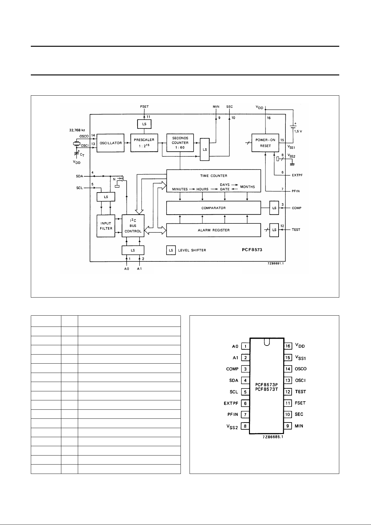
5 BLOCK DIAGRAM
Fig.1 Block diagram.
6 PINNING
SYMBOL PIN DESCRIPTION
A0 1 address input
A1 2 address input
COMP 3 comparator output
SDA 4 serial data line; I
2
C-bus
SCL 5 serial clock line; I
2
C-bus
EXTPF 6 enable power fail flag input
PFIN 7 power fail flag input
V
SS2
8 negative supply 2 (I2C interface)
MIN 9 one pulse per minute output
SEC 10 one pulse per second output
FSET 11 oscillator tuning output
TEST 12 test input; connect to V
SS2
if not in use
OSCI 13 oscillator input
OSCO 14 oscillator input/output
V
SS1
15 negative supply 1 (clock)
V
DD
16 common positive supply
Fig.2 Pinning diagram.

1997 Mar 28 5
Philips Semiconductors Product specification
Clock/calendar with Power Fail Detector PCF8573
7 FUNCTIONAL DESCRIPTION
7.1 Oscillator
The PCF8573 has an integrated crystal-controlled
oscillator which provides the timebase for the prescaler.
The frequency is determined by a single 32.76 kHz crystal
connected between OSCI and OSCO. A trimmer is
connected between OSCI and V
DD
.
7.2 Prescaler and time counter
The prescaler provides a 128 Hz signal at the FSET output
for fine adjustment of the crystal oscillator without loading
it. The prescaler also generates a pulse once a second to
advance the seconds counter. The carry of the prescaler
and the seconds counter are available at the outputs SEC,
MIN respectively, and are also readable via the I
2
C-bus.
The mark-to-space ratio of both signals is 1 : 1. The time
counter is advanced one count by the falling edge of output
signal MIN. A transition from HIGH-to-LOW of output
signal SEC triggers MIN to change state. The time counter
counts minutes, hours, days and months, and provides a
full calendar function which needs to be corrected only
once every four years - to allow for leap-year. Cycle
lengths are shown in Table 1.
7.3 Alarm register
The alarm register is a 24-bit memory. It stores the
time-point for the next setting of the status flag COMP.
Details of writing and reading of the alarm register are
included in the description of the characteristics of the
I
2
C-bus.
7.4 Comparator
The comparator compares the contents of the alarm
register and the time counter, each with a length of 24 bits.
When these contents are equal the flag COMP will be set
4 ms after the falling edge of MIN. This set condition
occurs once at the beginning of each minute. This
information is latched, but can be cleared by an instruction
via the I
2
C-bus. A clear instruction may be transmitted
immediately after the flag is set and will be executed. Flag
COMP information is also available at the output COMP.
The comparison may be based upon hours and minutes
only if the internal flag NODA (no date) is set. Flag NODA
can be set and cleared by separate instructions via the
I2C-bus, but it is undefined until the first set or clear
instruction has been received. Both COMP and NODA
flags are readable via the I2C-bus.
Table 1 Cycle length of the time counter
Note
1. During February of a leap-year the ‘Time Counter Days’ may be set to 29 by directly writing into it using the ‘execute
address’ function. Leap-years must be tracked by the system software.
UNIT NUMBER OF BITS COUNTING CYCLE
CARRY FOR
FOLLOWING UNIT
CONTENT OF MONTH
COUNTER
minutes 7 00 to 59 59 → 00
hours 6 00 to 23 23 → 00
days
(1)
6 01 to 28 28 → 01 2 (note 1)
or 29 → 01 2 (note 1)
01 to 30 30 → 01 4, 6, 9, 11
01 to 31 31 → 01 1, 3, 5, 7, 8, 10, 12
months 5 01 to 12 12 → 01

1997 Mar 28 6
Philips Semiconductors Product specification
Clock/calendar with Power Fail Detector PCF8573
7.5 Power on/power fail detection
If the voltage VDD− V
SS1
falls below a certain value the
operation of the clock becomes undefined. Thus a warning
signal is required to indicate that faultless operation of the
clock is not guaranteed. This information is latched in a
flag called POWF (Power Fail) and remains latched after
restoration of the correct supply voltage until a write
procedure with EXECUTE ADDRESS has been received.
The flag POWF can be set by an internally generated
power fail level-discriminator signal for application with
(V
DD
− V
SS1
) greater than V
TH1
, or by an externally
generated power fail signal for application with
(VDD− V
SS1
) less than V
TH1
. The external signal must be
applied to the input PFIN. The input stage operates with
signals of slow rise and fall times. Internally or externally
controlled POWF can be selected by input EXTPF as
shown in Table 2.
Table 2 Power fail selection
Note
1. 0 = V
SS1
(LOW); 1 = VDD (HIGH).
EXTPF
(1)
PFIN
(1)
FUNCTION
0 0 power fail is sensed internally
0 1 test mode
1 0 power fail is sensed externally
1 1 no power fail sensed
The external power fail control operates by absence of the
VDD− V
SS2
supply. Therefore the input levels applied to
PFIN and EXTPF must be within the range of VDD−V
SS1
.
A LOW level at PFIN indicates a power fail. POWF is
readable via the I2C-bus. A power-on reset for the I2C-bus
control is generated on-chip when the supply voltage
VDD− V
SS2
is less than V
TH2
.
7.6 Interface level shifters
The level shifters adjust the 5 V operating voltage
(V
DD
− V
SS2
) of the microcontroller to the internal supply
voltage (V
DD
− V
SS1
) of the clock/calendar. The oscillator
and counter are not influenced by the VDD− V
SS2
supply
voltage. If the voltage VDD− V
SS2
is absent (VDD=V
SS2
)
the output signal of the level shifter is HIGH because V
DD
is the common node of the VDD− V
SS2
and the VDD− V
SS1
supplies. Because the level shifters invert the input
signals, the internal circuit behaves as if a LOW signal is
present on the inputs. FSET, SEC, MIN and COMP are
CMOS push-pull output stages. The driving capability of
these outputs is lost when the supply voltage
VDD− V
SS2
=0.
1997 Mar 28 7
Philips Semiconductors Product specification
Clock/calendar with Power Fail Detector PCF8573
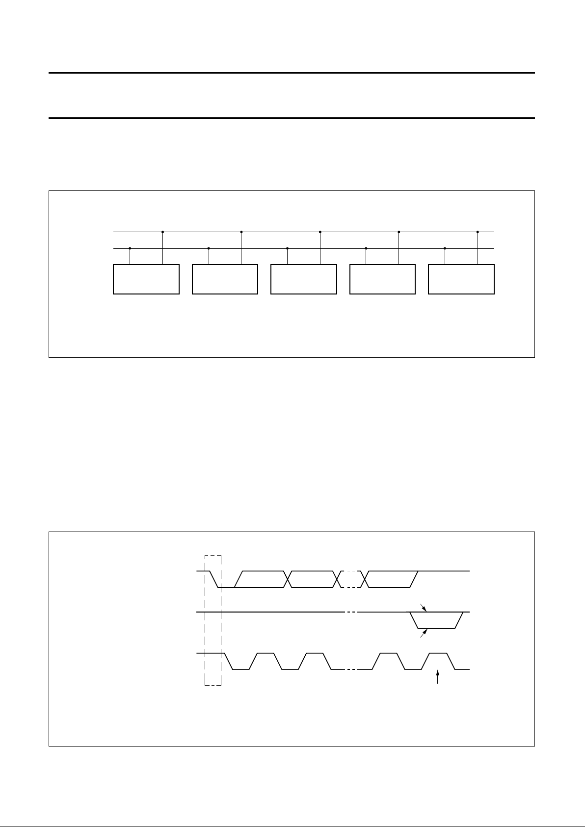
8 CHARACTERISTICS OF THE I2C-BUS
The I2C-bus is for 2-way, 2-line communication between different ICs or modules. The two lines are a serial data line
(SDA) and a serial clock line (SCL). Both lines must be connected to a positive supply via a pull-up resistor when
connected to the output stages of a device. Data transfer may be initiated only when the bus is not busy.
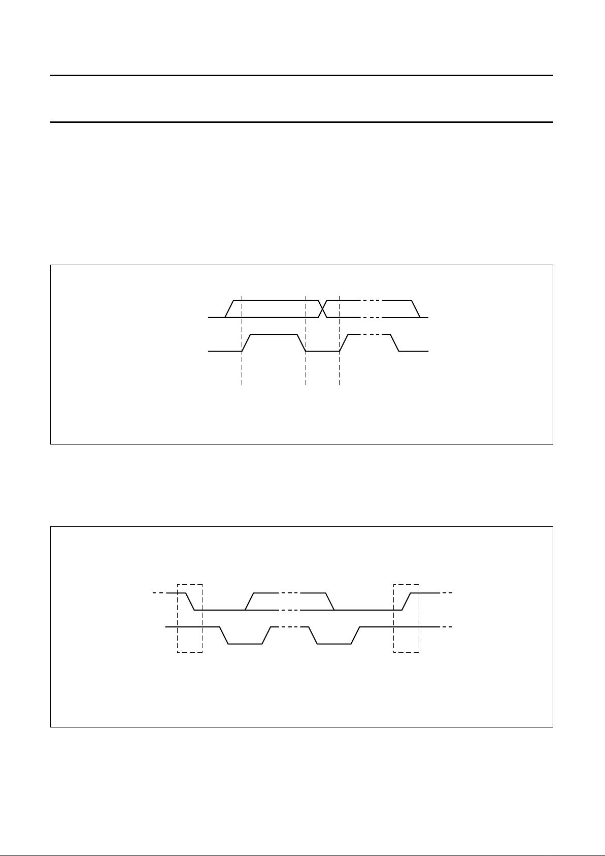
8.1 Bit transfer (see Fig.3)
One data bit is transferred during each clock pulse. The data on the SDA line must remain stable during the HIGH period
of the clock pulse as changes in the data line at this time will be interpreted as control signals.
8.2 Start and stop conditions (see Fig.4)
Both data and clock lines remain HIGH when the bus is not busy. A HIGH-to-LOW transition of the data line, while the
clock is HIGH is defined as the start condition (S). A LOW-to-HIGH transition of the data line while the clock is HIGH is
defined as the stop condition (P).
Fig.3 Bit transfer.
MBC621
data line
stable;
data valid
change
of data
allowed
SDA
SCL
Fig.4 Definition of start and stop conditions.
MBC622
SDA
SCL
P
STOP condition
SDA
SCL
S
START condition
1997 Mar 28 8
Philips Semiconductors Product specification
Clock/calendar with Power Fail Detector PCF8573
8.3 System configuration (see Fig.5)
A device generating a message is a ‘transmitter’, a device receiving a message is the ‘receiver’. The device that controls
the message is the ‘master’ and the devices which are controlled by the master are the ‘slaves’.
Fig.5 System configuration.
MBA605
MASTER
TRANSMITTER /
RECEIVER
SLAVE
RECEIVER
SLAVE
TRANSMITTER /
RECEIVER
MASTER
TRANSMITTER
MASTER
TRANSMITTER /
RECEIVER
SDA
SCL
8.4 Acknowledge (see Fig.6)
The number of data bytes transferred between the start
and stop conditions from transmitter to receiver is
unlimited. Each byte of eight bits is followed by an
acknowledge bit. The acknowledge bit is a HIGH level
signal put on the bus by the transmitter during which time
the master generates an extra acknowledge related clock
pulse. A slave receiver which is addressed must generate
an acknowledge after the reception of each byte. Also a
master receiver must generate an acknowledge after the
reception of each byte that has been clocked out of the
slave transmitter.
The device that acknowledges must pull down the SDA
line during the acknowledge clock pulse, so that the SDA
line is stable LOW during the HIGH period of the
acknowledge related clock pulse (set-up and hold times
must be taken into consideration). A master receiver must
signal an end of data to the transmitter by not generating
an acknowledge on the last byte that has been clocked
out of the slave. In this event the transmitter must leave the
data line HIGH to enable the master to generate a stop
condition, see Figs. 9 and 10.
Fig.6 Acknowledgment on the I2C-bus.
MBC602
S
START
CONDITION
9821
clock pulse for
acknowledgement
not acknowledge
acknowledge
DATA OUTPUT
BY TRANSMITTER
DATA OUTPUT
BY RECEIVER
SCL FROM
MASTER
 Loading...