

Philips PCF8563P, PCF8563T, PCF8563TS Datasheet

PCF8563
Real-time clock/calendar
16 April 1999 Product specification
1. General description
The PCF8563 is a CMOS real-time clock/calendar optimized for low power
consumption. A programmableclockoutput,interruptoutputandvoltage-low detector
are also provided. All address and data are transferred serially via a two-line
bidirectional I2C-bus. Maximum bus speed is 400 kbits/s. The built-in word address
register is incremented automatically after each written or read data byte.
2. Features
■ Provides year, month, day, weekday, hours, minutes and seconds based on
32.768 kHz quartz crystal
■ Century flag
■ Wide operating supply voltage range: 1.0 to 5.5 V
■ Low back-up current; typical 0.25 µA at VDD= 3.0 V and T
■ 400 kHz two-wire I2C-bus interface (at VDD= 1.8 to 5.5 V)
■ Programmable clock output for peripheral devices: 32.768 kHz, 1024 Hz,
32 Hz and 1 Hz
■ Alarm and timer functions
■ Voltage-low detector
■ Integrated oscillator capacitor
■ Internal power-on reset
■ I2C-bus slave address: read A3H; write A2H
■ Open drain interrupt pin.
amb
=25°C
3. Applications
■ Mobile telephones
■ Portable instruments
■ Fax machines
■ Battery powered products.
Philips Semiconductors
PCF8563
Real-time clock/calendar
4. Quick reference data
Table 1: Quick reference data
Symbol Parameter Conditions Min Max Unit
V
DD
I
DD
T
amb
T
stg
supply voltage operating mode I2C-bus inactive; T
2
C-bus active; f
I
= −40 to +85 °C
T
amb
supply current; timer and CLKOUT
disabled
f
= 400 kHz - 800 µA
SCL
= 100 kHz - 200 µA
f
SCL
= 0 Hz; T
f
SCL
V
V
DD
DD
amb
= 5 V - 550 nA
= 2 V - 450 nA
operating ambient temperature −40 +85 °C
storage temperature −65 +150 °C
=25°C 1.0 5.5 V
amb
= 400 kHz;
SCL
1.8 5.5 V
=25°C
5. Ordering information
Table 2: Ordering information
Type number Package
Name Description Version
PCF8563P DIP8 plastic dual in-line package; 8 leads (300 mil) SOT97-1
PCF8563T SO8 plastic small outline package; 8 leads; body width 3.9 mm SOT96-1
PCF8563TS TSSOP8 plastic thin shrink small outline package; 8 leads; body width 3.0 mm SOT505-1
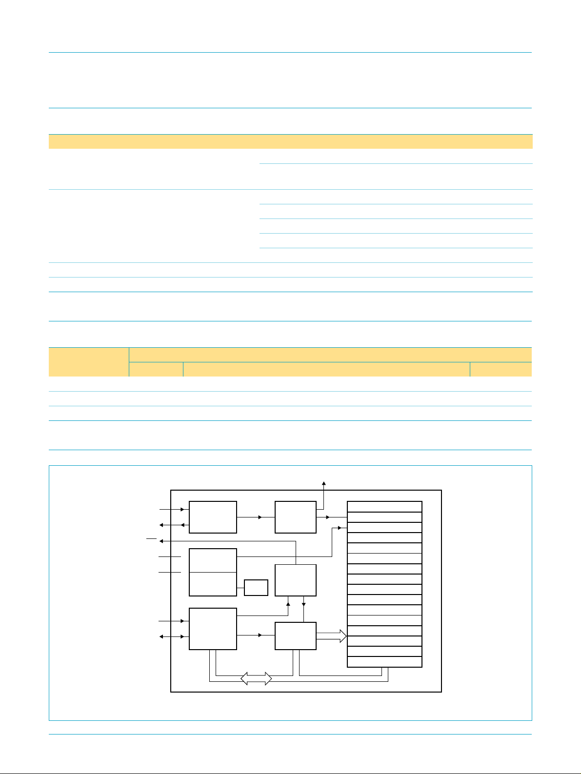
6. Block diagram
DIVIDER
LOGIC
CLKOUT
7
CONTROL/STATUS 1
1 Hz
CONTROL/STATUS 2
SECONDS/VL
MINUTES
HOURS
DAYS
WEEKDAYS
MONTHS/CENTURY
YEARS
MINUTE ALARM
HOUR ALARM
DAY ALARM
WEEKDAY ALARM
CLKOUT CONTROL
TIMER CONTROL
TIMER
0
1
2
3
4
5
6
7
8
9
A
B
C
D
E
F
handbook, full pagewidth
OSCI
OSCO
INT
V
SS
V
DD
SCL
SDA
1
2
3
4
8
6
5
OSCILLATOR
32.768 kHz
VOLTAGE
DETECTOR
OSCILLATOR
MONITOR
I2C-BUS
INTERFACE
POR
CONTROL
ADDRESS
REGISTER
MGM662
Fig 1. Block diagram.
9397 750 04855
Product specification 16 April 1999 2 of 30
© Philips Electronics N.V. 1999. All rights reserved.
Philips Semiconductors
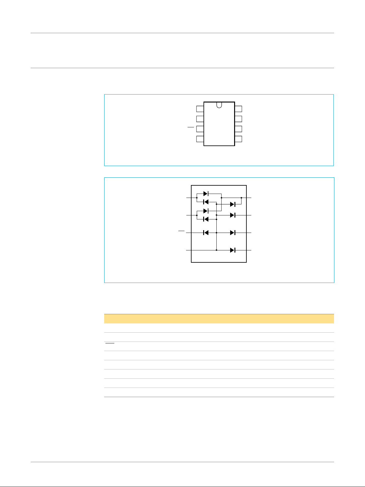
7. Pinning information
7.1 Pinning
PCF8563
Real-time clock/calendar
handbook, halfpage
OSCI
INT
V
SS
1
PCF8563P
2
PCF8563T
3
PCF8563TS
4
Fig 2. Pin configuration.
handbook, halfpage
1
OSCI
V
INT
SS
2
3
4
OSCO
PCF8563
Fig 3. Device diode protection diagram.
MGR885
8
7
6
5
MGR886
V
CLKOUTOSCO
SCL
SDA
8
7
6
5
DD
V
DD
CLKOUT
SCL
SDA
7.2 Pin description
Table 3: Pin description
Symbol Pin Description
OSCI 1 oscillator input
OSCO 2 oscillator output
INT 3 interrupt output (open-drain; active LOW)
V
SS
SDA 5 serial data I/O
SCL 6 serial clock input
CLKOUT 7 clock output (open-drain)
V
DD
9397 750 04855
Product specification 16 April 1999 3 of 30
4 ground
8 positive supply
© Philips Electronics N.V. 1999. All rights reserved.

Philips Semiconductors
8. Functional description
The PCF8563 contains sixteen 8-bit registers with an auto-incrementing address
register, an on-chip 32.768 kHz oscillator with an integrated capacitor, a frequency
divider which provides the source clock for the Real-Time Clock (RTC), a
programmable clock output, a timer, an alarm, a voltage-low detector and a 400 kHz
I2C-bus interface.
All 16 registers are designed as addressable 8-bit parallel registers although not all
bits are implemented. The first two registers (memory address 00H and 01H) are
used as control and/or status registers. The memory addresses 02H through 08H are
used as counters for the clock function (seconds up to year counters). Address
locations 09H through 0CH contain alarm registers which define the conditions for an
alarm. Address 0DH controls the CLKOUT output frequency. 0EH and 0FH are the
timer control and timer registers, respectively.
The Seconds, Minutes, Hours, Days, Months, Years as well as the Minute alarm,
Hour alarm and Day alarm registers are all coded in BCD format. The Weekdays and
Weekday alarm register are not coded in BCD format.
PCF8563
Real-time clock/calendar
When one of the RTC registers is read the contents of all counters are frozen.
Therefore, faulty reading of the clock/calendar during a carry condition is prevented.
8.1 Alarm function modes
By clearing the MSB (bit AE = Alarm Enable) of one or more of the alarm registers,
the corresponding alarm condition(s) will be active. In this way an alarm can be
generated from once per minute up to once per week. The alarm condition sets the
alarm flag, AF (bit 3 of Control/Status 2 register). The asserted AF can be used to
generate an interrupt (INT). Bit AF can only be cleared by software.
8.2 Timer
The 8-bit countdown timer (address 0FH) is controlled by the Timer Control register
(address 0EH; see Table 25). The Timer Control register selects one of 4 source
clock frequencies for the timer (4096, 64, 1, or1⁄60Hz), and enables/disables the
timer. The timer counts down from a software-loaded 8-bit binary value. At the end of
every countdown, the timer sets the timer flag TF (see Table 7). The timer flag TF can
only be cleared by software. The asserted timer flag TF can be used to generate an
interrupt (INT). The interrupt may be generated as a pulsed signal every countdown
period or as a permanently active signal which follows the condition of TF. TI/TP (see
Table 7) is used to control this mode selection. When reading the timer, the current
countdown value is returned.
8.3 CLKOUT output
A programmable square wave is availableat the CLKOUT pin. Operation is controlled
by the CLKOUT frequency register (address 0DH; see Table 23). Frequencies of
32.768 kHz (default), 1024, 32 and 1 Hz can be generated for use as a system clock,
microcontroller clock, input to a charge pump, or for calibration of the oscillator.
CLKOUT is an open-drain output and enabled at power-on. If disabled it becomes
high-impedance.
9397 750 04855
Product specification 16 April 1999 4 of 30
© Philips Electronics N.V. 1999. All rights reserved.
Philips Semiconductors
8.4 Reset
The PCF8563 includes an internal reset circuit which is active whenever the oscillator
is stopped. In the reset state the I2C-bus logic is initialized and all registers, including
the address pointer, are cleared with the exception of bits FE, VL, TD1, TD0, TESTC
and AE which are set to logic 1.
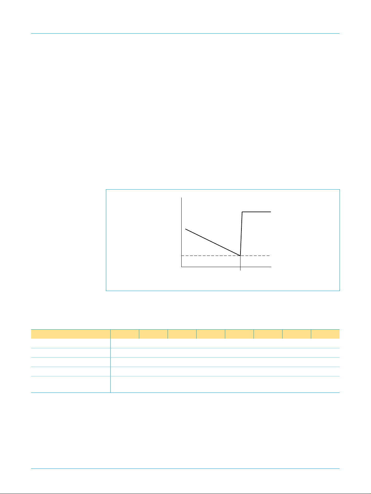
8.5 Voltage-low detector and clock monitor
PCF8563
Real-time clock/calendar
The PCF8563 has an on-chip voltage-low detector. When VDD drops below V
VL bit (Voltage Low, bit 7 in the Seconds register) is set to indicate that reliable
clock/calendar information is no longer guaranteed. The VL flag can only be cleared
by software.
The VL bit is intended to detect the situation when VDD is decreasing slowly for
example under battery operation. Should VDDreach V
before power is re-asserted
low
then the VL bit will be set. This will indicate that the time may be corrupted.
handbook, halfpage
V
DD
V
low
Fig 4. Voltage-low detection.
period of battery
operation
VL set
MGR887
normal power
operation
t
8.6 Register organization
low
the
Table 4: Registers overview
Bit positions labelled as ‘−’are not implemented; those labelled with ‘0’ should always be written with logic 0.
Address Register name Bit 7 Bit 6 Bit 5 Bit 4 Bit 3 Bit 2 Bit 1 Bit 0
00H Control/Status 1 TEST1 0 STOP 0 TESTC 0 0 0
01H Control/Status 2 0 0 0 TI/TP AF TF AIE TIE
0DH CLKOUT frequency FE −−−−−FD1 FD0
0EH Timer control TE −−−−−TD1 TD0
0FH Timer countdown
value
9397 750 04855
Product specification 16 April 1999 5 of 30
<timer countdown value>
© Philips Electronics N.V. 1999. All rights reserved.

Philips Semiconductors
PCF8563
Real-time clock/calendar
Table 5: BCD formatted registers overview
Bit positions labelled as ‘−’are not implemented.
Address Register name BCD format tens nibble BCD format units nibble
Bit 7 Bit 6 Bit 5 Bit 4 Bit 3 Bit 2 Bit 1 Bit 0
3
2
02H Seconds VL <seconds 00 to 59 coded in BCD>
03H Minutes − <minutes 00 to 59 coded in BCD>
04H Hours −− <hours 00 to 23 coded in BCD>
05H Days −− <days 01 to 31 coded in BCD>
06H Weekdays −−−−− <weekdays 0 to 6 >
07H Months/Century C −− <months 01 to 12 coded in BCD>
08H Years <years 00 to 99 coded in BCD>
09H Minute alarm AE <minute alarm 00 to 59 coded in BCD>
0AH Hour alarm AE − <hour alarm 00 to 23 coded in BCD>
0BH Day alarm AE − <day alarm 01 to 31 coded in BCD>
0CH Weekday alarm AE −−−− <weekday alarm 0 to 6 >
2
2
1
2
0
2
3
2
2
2
1
2
0
2
[1]
[1]
[1] Not coded in BCD.
8.6.1 Control/Status 1 register
Table 6: Control/Status 1 register bits description (address 00H)
Bit Symbol Description
7 TEST1 TEST1 = 0; normal mode.
TEST1 = 1; EXT_CLK test mode; see Section 8.7.
5 STOP STOP = 0; RTC source clock runs.
STOP = 1; all RTC divider chain flip-flops are asynchronously set
to logic 0; the RTC clock is stopped (CLKOUT at 32.768 kHz is still
available).
3 TESTC TESTC = 0; power-on reset override facility is disabled (set to logic 0
for normal operation).
TESTC = 1; power-on reset override is enabled.
6, 4, 2 to 0 0 By default set to logic 0.
9397 750 04855
Product specification 16 April 1999 6 of 30
© Philips Electronics N.V. 1999. All rights reserved.

Philips Semiconductors
8.6.2 Control/Status 2 register
Table 7: Description of Control/Status 2 register bits description (address 01H)
Bit Symbol Description
7 to 5 0 By default set to logic 0.
4 TI/TP TI/TP = 0: INT is active when TF is active (subject to the status of TIE).
3 AF When an alarm occurs, AF is set to logic 1. Similarly, at the end of a
2TF
1 AIE Bits AIE and TIE activate or deactivate the generation of an interrupt
0 TIE
PCF8563
Real-time clock/calendar
TI/TP = 1: INT pulses active according to Table 8 (subjectto the status
of TIE). Note that if AF and AIE are active then INT will be permanently
active.
timer countdown, TF is set to logic 1. These bits maintain their value
until overwritten by software. If both timer and alarm interrupts are
required in the application, the source of the interrupt can be
determined by reading these bits. To prevent one flag being
overwritten while clearing another, a logic AND is performed during a
write access. See Table 9 for the value descriptions of bits AF and TF.
when AF or TF is asserted, respectively.The interrupt is the logical OR
of these two conditions when both AIE and TIE are set.
AIE = 0: alarm interrupt disabled; AIE = 1: alarm interrupt enabled.
TIE = 0: timer interrupt disabled; TIE = 1: timer interrupt enabled.
Table 8:
Source clock (Hz) INT
4096
64
1
1
⁄
60
[1] TF and INT become active simultaneously.
[2] n = loaded countdown timer value. Timer stopped when n = 0.
INT operation (bit TI/TP = 1)
[1]
period (s)
[2]
n
=1 n>1
1
⁄
8192
1
⁄
128
1
⁄
64
1
⁄
64
Table 9: Value descriptions for bits AF and TF
R/W Bit: AF Bit: TF
Value Description Value Description
Read 0 alarm flag inactive 0 timer flag inactive
1 alarm flag active 1 timer flag active
Write 0 alarm flag is cleared 0 timer flag is cleared
1 alarm flag remains unchanged 1 timer flag remains unchanged
1
⁄
4096
1
⁄
64
1
⁄
64
1
⁄
64
9397 750 04855
Product specification 16 April 1999 7 of 30
© Philips Electronics N.V. 1999. All rights reserved.

Philips Semiconductors
8.6.3 Seconds, Minutes and Hours registers
Table 10: Seconds/VL register bits description (address 02H)
Bit Symbol Description
7 VL VL = 0: reliable clock/calendar information is guaranteed;
6 to 0 <seconds> These bits represent the current seconds value coded in BCD
Table 11: Minutes register bits description (address 03H)
Bit Symbol Description
7 − not implemented
6 to 0 <minutes> These bits represent the current minutes value coded in BCD
Table 12: Hours register bits description (address 04H)
Bit Symbol Description
7 to 6 − not implemented
5 to 0 <hours> These bits represent the current hours value coded in BCD format;
PCF8563
Real-time clock/calendar
VL = 1: reliable clock/calendar information is no longer
guaranteed.
format; value = 00 to 59.
Example: <seconds> = 101 1001, represents the value 59 s.
format; value = 00 to 59.
value=00to23.
8.6.4 Days, Weekdays, Months/Century and Years registers
Table 13: Days register bits description (address 05H)
Bit Symbol Description
7 to 6 − not implemented
5 to 0 <days> These bits represent the current day value coded in BCD format;
value = 01 to 31.
The PCF8563 compensates for leap years by adding a 29th day to
February if the year counter contains a value which is exactly
divisible by 4, including the year ‘00’.
Table 14: Weekdays register bits description (address 06H)
Bit Symbol Description
7 to 3 − not implemented
2 to 0 <weekdays> These bits represent the current weekday value 0 to 6;
see Table 15.
These bits may be re-assigned by the user.
9397 750 04855
Product specification 16 April 1999 8 of 30
© Philips Electronics N.V. 1999. All rights reserved.

Philips Semiconductors
Table 15: Weekday assignments
Day Bit 2 Bit 1 Bit 0
Sunday 0 0 0
Monday 0 0 1
Tuesday 0 1 0
Wednesday 0 1 1
Thursday 1 0 0
Friday 1 0 1
Saturday 1 1 0
Table 16: Months/Century register bits description (address 07H)
Bit Symbol Description
7 C Century bit. C = 0; indicates the century is 20xx.
6to5 − not implemented
4 to 0 <months> These bits represents the current month value coded in BCD format;
PCF8563
Real-time clock/calendar
C = 1; indicates the century is 19xx. ‘xx’ indicates the value held in the
Years register; see Table 18.
This bit is toggled when the Years register overflows from 99 to 00.
These bits may be re-assigned by the user.
value = 01 to 12; see Table 17.
Table 17: Month assignments
Month Bit 4 Bit 3 Bit 2 Bit 1 Bit 0
January00001
February00010
March 00011
April 00100
May 00101
June 00110
July 00111
August 01000
September 01001
October 10000
November 10001
December 10010
Table 18: Years register bits description (address 08H)
Bit Symbol Description
7 to 0 <years> This register represents the current year value coded in BCD
format; value = 00 to 99.
9397 750 04855
Product specification 16 April 1999 9 of 30
© Philips Electronics N.V. 1999. All rights reserved.
 Loading...