


INTEGRATED CIRCUITS
DATA SH EET
PCB2421
1K dual mode serial EEPROM
Preliminary specification
Supersedes data of 1995 Oct 11
File under Integrated Circuits, IC12
1997 Apr 01

Philips Semiconductors Preliminary specification
1K dual mode serial EEPROM PCB2421
CONTENTS
1 FEATURES
2 GENERAL DESCRIPTION
3 ORDERING INFORMATION
4 BLOCK DIAGRAM
5 PINNING
6 FUNCTIONAL DESCRIPTION
6.1 Transmit-only mode (DDC1)
6.2 Initialization procedure
6.3 Bidirectional mode (DDC2B, I2C-bus mode)
6.3.1 Bidirectional mode bus characteristics
6.3.2 Bus not busy (A)
6.3.3 Start condition (B)
6.3.4 Stop condition (C)
6.3.5 Data valid (D)
6.3.6 Acknowledge
6.3.7 Slave address
6.4 Write operation
6.4.1 Byte write
6.4.2 Page write
6.5 Acknowledge polling
6.6 Write protection
6.7 Read operation
6.7.1 Current address read
6.7.2 Random read
6.7.3 Sequential read
6.8 Pin description
6.8.1 SDA
6.8.2 SCL
6.8.3 VCLK
6.8.4 WP
6.8.5 Test
6.8.6 n.c.
7 LIMITING VALUES
8 DC CHARACTERISTICS
9 EEPROM CHARACTERISTICS
10 AC CHARACTERISTICS
11 APPLICATION INFORMATION
11.1 Diode protection
11.2 Functional compatibility with microchip 24CL21
dual mode EEPROM
12 PACKAGE OUTLINES
13 SOLDERING
13.1 Introduction
13.2 DIP
13.2.1 Soldering by dipping or by wave
13.2.2 Repairing soldered joints
13.3 SO
13.3.1 Reflow soldering
13.3.2 Wave soldering
13.3.3 Repairing soldered joints
14 DEFINITIONS
15 LIFE SUPPORT APPLICATIONS
16 PURCHASE OF PHILIPS I2C COMPONENTS
1997 Apr 01 2
Philips Semiconductors Preliminary specification
1K dual mode serial EEPROM PCB2421
1 FEATURES
• Single supply with operation 4.5 to 5.5 V
• Completely implements DDC1/DDC2B interface for
monitor identification
• Low power CMOS technology
• Two-wire I2C-bus interface
• Self-timed write cycle (including auto-erase)
• Page-write buffer for up to 8 bytes
• Write-protect pin
• 100 kHz I2C-bus compatibility
• Designed for 10000 erase/write cycles minimum
• Data retention greater than 10 years
• 8-pin DIP and SO package
• Temperature range 0 to +70 °C.
3 ORDERING INFORMATION
TYPE NUMBER
NAME DESCRIPTION VERSION
PCB2421P DIP8 plastic dual in-line package; 8 leads (300 mil) SOT97-1
PCB2421T SO8 plastic small outline package; 8 leads; body width 3.9 mm SOT96-1
2 GENERAL DESCRIPTION
The Philips PCB2421 is a 128 × 8-bit dual mode serial
Electrically Erasable PROM (EEPROM).
This device is designed for use in applications requiring
storage and serial transmission of configuration and
control information. Two modes of operation have been
implemented: transmit-only mode (DDC1 mode) and
bidirectional mode (DDC2B, or I2C-bus mode). Upon
power-up, the device will be in the transmit-only mode,
sending a serial bitstream of the entire memory array
contents, clocked by the VCLK pin. A valid HIGH-to-LOW
transition on the SCL pin will cause the device to enter the
bidirectional mode, with byte selectable read/write
capability of the memory array. The PCB2421 is available
in a standard 8-pin dual in-line and 8-pin small outline
package operating in a commercial temperature range.
PACKAGE
1997 Apr 01 3
Philips Semiconductors Preliminary specification
1K dual mode serial EEPROM PCB2421
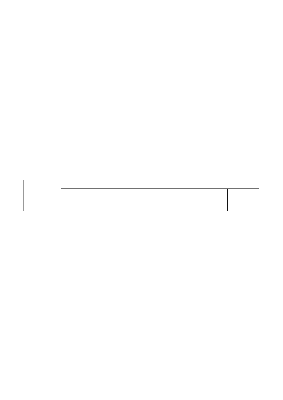
4 BLOCK DIAGRAM
V
V
ok, full pagewidth
SS
DD
48
WP
SDA
SCL
VCLK
3
5
6
7
I/O
CONTROL
LOGIC
MEMORY
CONTROL
LOGIC
PCB2421
n.c.
TEST
(1) Factory use only.
2
1
(1)
Fig.1 Block diagram.
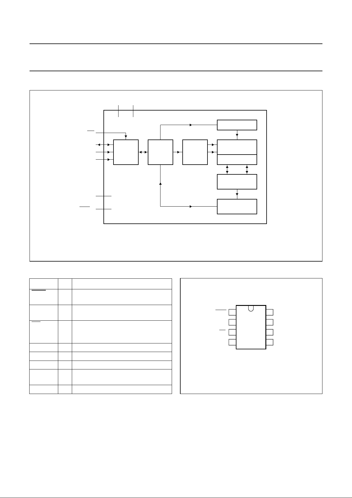
5 PINNING
SYMBOL PIN DESCRIPTION
TEST 1 factory use only: must be tied to VDD;
may not be left open-circuit
n.c. 2 may be tied to V
, VDD, or left
SS
open-circuit
WP 3 write protect input (LOW = write
protected, HIGH = not write protected);
may not be left open-circuit
V
SS
4 ground
SDA 5 serial data input/output
SCL 6 serial clock input/output (DDC2B)
VCLK 7 serial clock input (transmit-only mode,
DDC1)
V
DD
8 supply voltage
X
DECODER
handbook, halfpage
HV GENERATOR
EEPROM
ARRAY
PAGE LATCHES
Y
DECODER
SENSE AMPLIFIER
R/W CONTROL
MBG271
1
TEST
2
n.c. VCLK
WP SCL
V
SS
3
4
PCB2421
8
7
6
5
MBG272
Fig.2 Pin configuration.
V
DD
SDA
1997 Apr 01 4

Philips Semiconductors Preliminary specification
1K dual mode serial EEPROM PCB2421
6 FUNCTIONAL DESCRIPTION
The PCB2421 operates in two modes, the transmit-only
mode (DDC1) and the bidirectional mode (DDC2, or
I2C-bus mode). There is a separate two-wire protocol to
support each mode, each having a separate clock input
and sharing a common data line (SDA). The device enters
the transmit-only mode (DDC1) upon power-up. In this
mode the device transmits data bits on the SDA pin in
response to a clock signal on the VCLK pin. The device will
remain in this mode until a valid HIGH-to-LOW transition is
placed on the SCL input. When a valid transition on SCL is
recognized, the device will switch into the bidirectional
mode (see Fig.3). The only way to switch the device back
to the transmit-only mode (DDC1) is to remove power from
the device.
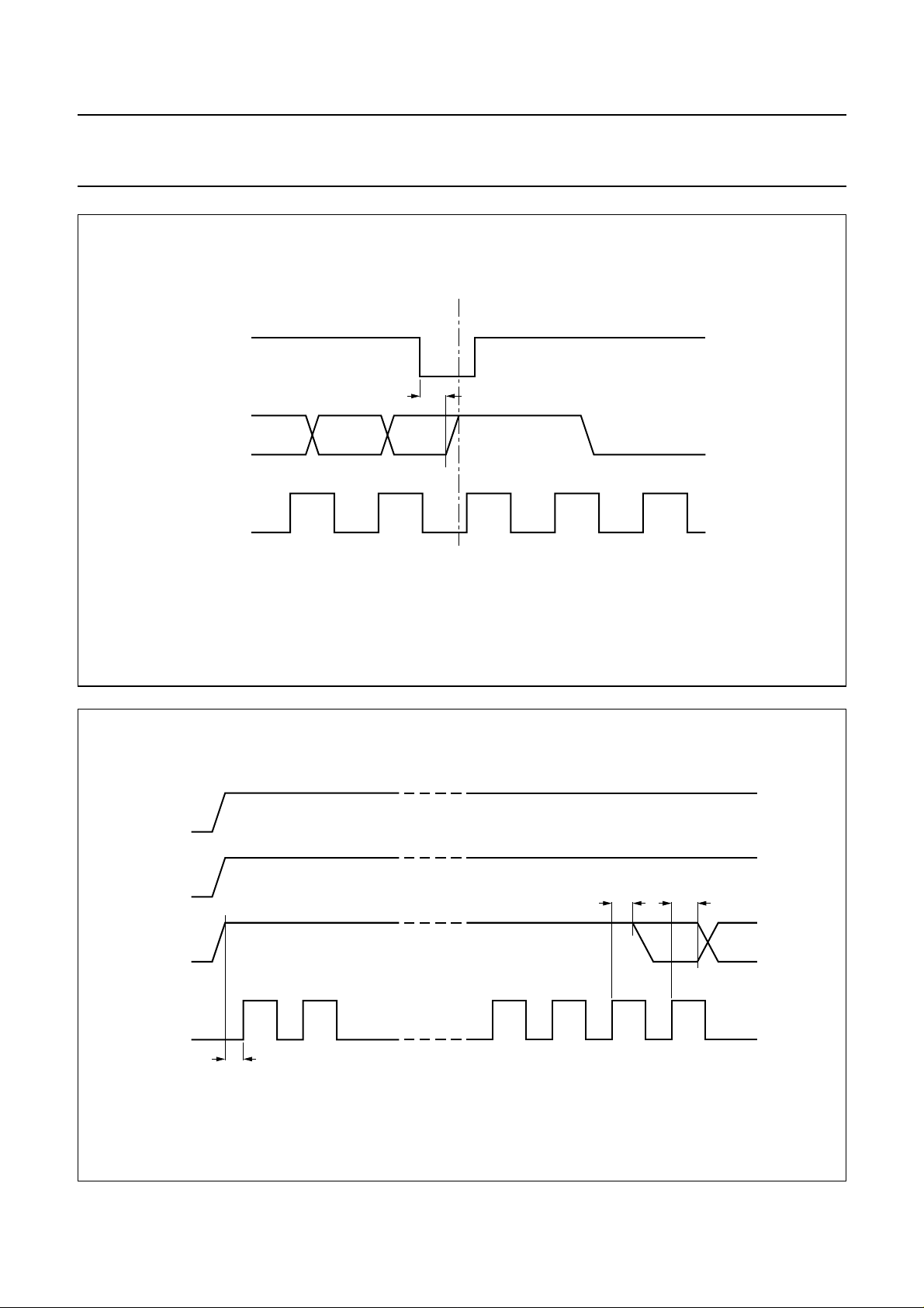
6.1 Transmit-only mode (DDC1)
The device will power-up in the transmit-only mode. This
mode supports a unidirectional two-wire protocol for
transmission of the contents of the memory array
(see Fig.12). The PCB2421 requires that it be initialized
prior to valid data being sent in the transmit-only mode
(see Section “Initialization procedure”, and Fig.4).
In this mode, data is transmitted on the SDA pin in 8-bit
bytes, each byte followed by a ninth clock pulse during
which time SDA is left high-impedance. The clock source
for the transmit-only mode is provided on the VCLK pin;
a data bit is output on the rising edge on this pin. The 8 bits
in each byte are transmitted most significant bit first. Each
byte within the memory array will be output in sequence.
When the last byte in the memory array is transmitted, the
output will wrap around to the first location and continue.
The bidirectional mode clock (SCL) pin must be held HIGH
for the device to remain in the transmit-only mode.
When the device has been switched into the bidirectional
mode, the VCLK input is disregarded. This mode supports
a two-wire bidirectional data transmission protocol
2
(I
C-bus protocol). In the I2C-bus protocol, a device that
sends data on the bus is defined to be the transmitter, and
a device that receives data from the bus is defined to be
the receiver. The bus must be controlled by a master
device that generates the bidirectional mode clock,
controls access to the bus, and generates the START and
STOP conditions, while the PCB2421 acts as slave. Both
master and slave can operate as transmitter or receiver,
but the master device determines which mode is activated.
6.3.1 B
IDIRECTIONAL MODE BUS CHARACTERISTICS
The following bus protocol has been defined:
• Data transfer may be initiated only when the bus is not
busy
• During data transfer, the data line must remain stable
whenever the clock line is HIGH. Changes in the data
line while the clock line is HIGH will be interpreted as a
START or STOP condition.
Accordingly, the following bus conditions have been
defined (see Fig.6).
6.3.2 B
US NOT BUSY (A)
Both data (SDA) and clock (SCL) lines remain HIGH.
6.3.3 S
TART CONDITION (B)
A HIGH-to-LOW transition of the SDA line while SCL is
HIGH determines a START condition. All commands must
be preceded by a START condition.
6.3.4 S
TOP CONDITION (C)
6.2 Initialization procedure
At power-on, after VDD has stabilized, the device will be in
the transmit-only mode. Nine clock cycles on the VCLK pin
must be given to the device for it to perform internal
synchronization. During this period, the SDA pin will be in
a high-impedance state. On the rising edge of the tenth
clock cycle, the device will output the first valid data bit
which will be the most significant bit of a byte. The device
will power-up with address pointer at 00H (see Fig.4).
2
6.3 Bidirectional mode (DDC2B, I
C-bus mode)
The PCB2421 can be switched into the bidirectional mode
(see Fig.3) by applying a valid HIGH-to-LOW transition on
the bidirectional mode clock (SCL).
1997 Apr 01 5
A LOW-to-HIGH transition of the SDA line while SCL is
HIGH determines a STOP condition. All operations must
be ended with a STOP condition.
6.3.5 D
ATA VALID (D)
The state of the data line represents valid data when, after
a START condition, the data line is stable for the duration
of the HIGH period of the clock signal. The data on the line
must be changed during the LOW period of the clock
signal. There is one clock pulse per bit of data. Each data
transfer is initiated with a START condition and terminated
with a STOP condition. The maximum number of data
bytes transferred between the START and STOP
conditions during a write operation is 8 bytes (see Section
“Page write” and Fig.5).

Philips Semiconductors Preliminary specification
1K dual mode serial EEPROM PCB2421
The maximum number of data bytes transferred between
START and STOP conditions during a read operation is
unlimited.
6.3.6 A
CKNOWLEDGE
The PCB2421, when addressed in DDC2B mode, is
obliged to generate an acknowledge after the reception of
each byte. The master device must generate an extra (9th)
clock pulse which is associated with this acknowledge bit.
The PCB2421 does not generate an acknowledge if an
internal programming cycle is in progress (SDA line is left
HIGH during the 9th clock pulse). The PCB2421 generates
an acknowledge by pulling down the SDA line during the
acknowledge pulse in such a way that the SDA line is
stable LOW during the HIGH period of the acknowledge
related clock pulse. Set-up and hold times must also be
taken into account. The master receiver must signal an
end of data to the PCB2421 by not generating an
acknowledge bit on the last byte that has been clocked out
of the slave transmitter. In this case, the slave transmitter
PCB2421 must leave the data line HIGH to enable the
master to generate the STOP condition.
6.3.7 S
LAVE ADDRESS
and will be written into the address pointer of the
PCB2421. After receiving another acknowledge signal
from the PCB2421, the master device will transmit the data
word to be written into the addressed memory location.
The PCB2421 acknowledges again and the master
generates a STOP condition. This initiates the internal
write cycle, and during this time the PCB2421 will not
generate acknowledge signals.
6.4.2 P
AGE WRITE
For a page write, the write control byte, word address, and
the first data byte are transmitted to the PCB2421 in the
same way as in a single byte write. But instead of
generating a STOP condition the master transmits up to
eight data bytes to the PCB2421 which are temporarily
stored in the on-chip page buffer and will be written into the
memory after the master has transmitted a STOP
condition. After the receipt of each word, the three lower
order address pointer bits are internally incremented by
one. The higher order four bits of the word address remain
constant. A maximum of 8 bytes can be written in one
operation. As with the byte write operation, once the STOP
condition is received an internal write cycle will begin
(see Figs 5 and 8).
After generating a START condition, the bus master
transmits the slave address (MSB first) consisting of a 7-bit
device address (1010000) for the PCB2421. The eighth bit
of the slave address determines if the master device wants
to read or write to the PCB2421 (R/W bit) (see Fig.7).
The PCB2421 monitors the bus for its corresponding slave
address all the time. It generates an acknowledge bit if the
slave address was true and it is not in a programming
mode.
Table 1 Slave address
OPERATION SLAVE ADDRESS R/
W
Read 1010000 1
Write 1010000 0
6.4 Write operation
6.4.1 B
YTE WRITE
Following the START condition from the master, the
device address (7 bits), and the R/W bit (logic LOW for
write) is placed on the bus by the master transmitter. This
indicates to the addressed slave receiver that a byte with
a word address will follow after it has generated an
acknowledge bit during the ninth clock cycle. Therefore the
next byte transmitted by the master is the word address
6.5 Acknowledge polling
Since the device will not acknowledge during a write cycle,
this can be used to determine when the cycle is complete
(this feature can be used to maximize bus throughput).
Once the STOP condition for a write command has been
issued from the master, the device initiates the internally
timed write cycle. Acknowledge (ACK) polling can be
initiated immediately. This involves the master sending a
START condition followed by the control byte for a write
command (R/
W = 0). If the device is still busy with the write
cycle, then no ACK will be returned. If the cycle is
complete, then the device will return the ACK and the
master can then proceed with the next read or write
command. See Fig.9 for flow diagram.
6.6 Write protection
Pin 3 is a write protect input (
WP). In the DDC1 mode, the
PCB2421 can only be read according to the DDC1
protocol, hence the WP input has no effect in this mode.
In the DDC2B mode, whenWP is connected to ground, the
entire EEPROM is write-protected, regardless of other pin
states. When connected to VDD, write-protection is
disabled and the EEPROM may be programmed. WP may
not be left open-circuit.
1997 Apr 01 6

Philips Semiconductors Preliminary specification
1K dual mode serial EEPROM PCB2421
Table 2 Mode configurations
DDC
DCC1 X
WP MODE
(1)
R
DCC2 1 R/W
0R
Note
1. Where X = don’t care.
6.7 Read operation
Read operations are initiated in the same way as write
operations with the exception that the R/W bit of the slave
address is set to logic 1. There are three basic types of
read operations: current address read, random read, and
sequential read.
6.7.1 C
URRENT ADDRESS READ
The PCB2421 contains an address counter that maintains
the address of the last word accessed, internally
incremented by one. Therefore, if the previous access
(either a read or write operation) was to address ‘n’, the
next current address read operation would access data
from address n + 1. Upon receipt of the slave address with
R/W set to logic 1, the PCB2421 issues an acknowledge
and transmits the eight bit data word. The master will not
acknowledge the transfer but does generate a STOP
condition and the PCB2421 discontinues transmission
(see Fig.10).
6.7.2 R
ANDOM READ
Random read operations allow the master to access any
memory location in a random manner. To perform this type
of read operation, the word address must first be set. This
is done by sending the word address to the PCB2421 as
part of a normal write operation. After the word address is
sent, the master generates a REPEATED START
condition following the acknowledge. This terminates the
write operation, but not before the internal address pointer
is set. The master then issues the control byte again but
with the R/W bit set to logic 1. The PCB2421 will then issue
an acknowledge and transmits the 8-bit data word.
The master will not acknowledge the transfer but does
generate a STOP condition and the PCB2421
discontinues transmission (see Fig.11).
6.7.3 S
EQUENTIAL READ
Sequential reads are initiated in the same way as a
random read except that after the PCB2421 transmits the
first data byte, the master issues an acknowledge as
opposed to a STOP condition in a random read.
This directs the PCB2421 to transmit the next sequentially
addressed 8-bit word. To provide sequential reads the
PCB2421 contains an internal address pointer which is
incremented by one at the completion of each operation.
This address pointer allows the entire memory contents to
be serially read during one operation.
6.8 Pin description
6.8.1 SDA
This pin is used to transfer addresses and data into and
out of the device, when the device is in the bidirectional
(I2C-bus, DDC2B) mode. In the transmit-only mode
(DDC1), which only allows data to be read from the device,
data is also transferred on the SDA pin. This pin is an
open-drain terminal, therefore the SDA bus requires a
pull-up resistor connected to VDD (typically 10 kΩ for
100 kHz). See brochure
(order no. 9398 393 40011) or
“The I2C-bus and how to use it”
“Data Handbook IC12”
.
6.8.2 SCL
This pin is the clock input for the bidirectional mode
2
(I
C-bus, DDC2B), and is used to synchronize data
transfer to and from the device. It is also used as the
signalling input to switch the device from the transmit-only
mode to the bidirectional mode. It must remain HIGH for
the chip to continue operation in the transmit-only mode
(DDC1).
6.8.3 VCLK
This pin is the clock input for the transmit-only mode
(DDC1). In the transmit-only mode, each bit is clocked out
on the rising edge of this signal. In DDC2B mode, this input
is a don’t care.
6.8.4
WP
This pin is used to inhibit writing of the EEPROM. When
this pin is connected to ground, writing of the EEPROM is
inhibited. When connected to VDD (and VCLK = VDD), the
EEPROM can be programmed. WP may not be left
open-circuit. WP input is a ‘don’t care’ in DDC1 mode.
6.8.5
TEST
Pins 1 is a TEST pin for factory use only. It must be
connected to VDD in the application.
6.8.6
N.C.
This pin has no connection and may be tied to VSS, VDD or
left open-circuit.
1997 Apr 01 7
Philips Semiconductors Preliminary specification
1K dual mode serial EEPROM PCB2421
handbook, full pagewidth
SCL
SDA
VCLK
transmit only mode
(DDC1)
t
VHZ
bidirectional mode
Fig.3 Mode transition diagram.
(DDC2)
MBG275
book, full pagewidth
V
DD
SCL
SDA
VCLK
high-impedance for 9 clock cycles
t
VPU
Fig.4 Device initialization diagram.
1997 Apr 01 8
t
VAA
t
VAA
bit 8 bit 7
11109812
MBG276
 Loading...