

Philips PCA9559 Datasheet

INTEGRATED CIRCUITS
PCA9559
5-bit multiplexed/1-bit latched 6-bit I
EEPROM
Product specification
Supersedes data of 1999 Oct 20
2
C
2000 Jan 31

Philips Semiconductors Product specification
PCA95595-bit multiplexed/1-bit latched 6-bit I2C EEPROM
FEA TURES
PIN CONFIGURATION
•5-bit 2-to-1 multiplexer, 1-bit latch
2
C SCL
•6-bit internal non-volatile register
•Internal non-volatile register programmable and readable via I
•Override input forces all outputs to logic 0
•5 open drain multiplexed outputs
•1 open drain non-multiplexed (latched) output
•5V and 2.5V tolerant inputs
•Useful for ‘jumperless’ configuration of PC motherboards
•2 address pins, allowing up to 4 devices on the I
2
C bus
2
C bus
I
I
MUX_IN A
MUX_IN B
MUX_IN C
MUX_IN D
MUX_IN E
2
C SDA
GND
1
2
A1
3
4
A0
5
6
7
8
9
10
DESCRIPTION
The primary function of the 5-bit multiplexer, 1-bit latch is to enable
system configuration.
ORDERING INFORMATION
PACKAGES TEMPERATURE RANGE ORDER CODE DRAWING NUMBER
20-Pin Plastic TSSOP 0°C to +70°C PCA9559 PW DH SOT360-1
FUNCTIONAL DESCRIPTION
When the MUX_SELECT signal is logic 0, the multiplexer will select
the data from the non-volatile register to drive on the MUX_OUT
pins. When the MUX_SELECT signal is logic 1, the multiplexer will
select the MUX_IN lines to drive on the MUX_OUT pins. The
MUX_SELECT signal is also used to latch the NON_MUXED_OUT
signal which outputs data from the non-volatile register. The
NON_MUXED_OUT signal latch is transparent when MUX_SELECT
is in a logic 0 state, and will latch data when MUX_SELECT is in a
logic 1 state. When the active-LOW OVERRIDE# signal is set to
logic 0 and the MUX_SELECT signal is at a logic 0, all outputs will
be driven to logic 0. This information is summarized in Table 1.
The Write Protect (WP) input is used to control the ability to write the
contents of the 6-bit non-volatile register. If the WP signal is logic 0,
2
the I
C bus will be able to write the contents of the non-volatile
register. If the WP signal is logic 1, data will not be allowed to be
written into the non-volatile register.
The factory default for the contents of the non-volatile register are all
logic 0. These stored values can be read or written using the I
bus (described in the next section).
The OVERRIDE#, WP, MUX_IN, and MUX_SELECT signals have
internal pullup resistors. See the DC and AC Characteristics for
hysteresis and signal spike suppression figures.
2
C
FUNCTION TABLE
OVERRIDE# MUX_SELECT
0 0 All 0’s All 0’s
0 1
1 0
1 1
NOTE:
1. NON_MUXED_OUT state will be the value present on the output
at the time of the MUX_SELECT input transitioned from a logic 0
to a logic 1 state.
MUX_OUT
OUTPUTS
From non-
20
19
18
17
16
15
14
13
12
11
MUX_IN
inputs
volatile
register
MUX_IN
inputs
V
WP
OVERRIDE #
NON_MUXED_OUT
MUX_OUT A
MUX_OUT B
MUX_OUT C
MUX_OUT D
MUX_OUT E
MUX_SELECT
CC
SW00216
NON_MUXED_OUT
OUTPUT
Latched
NON_MUXED
From non-volatile
register
From non-volatile
register
_OUT
1
2000 Jan 31 853-2181 23063
2
Philips Semiconductors Product specification
PCA95595-bit multiplexed/1-bit latched 6-bit I2C EEPROM
PIN DESCRIPTION
PIN
NUMBER
1 I2C SCL Serial I2C bus clock
2 I2C SDA Serial bi-directional I2C bus data
3 A1 Address A1
4 A0 Address A0
5 MUX_IN A
6 MUX_IN B
7 MUX_IN C
8 MUX_IN D
9 MUX_IN E
10 GND Ground
11 MUX_SELECT Selects MUX_IN inputs or register contents for MUX_OUT outputs
12 MUX_OUT E
13 MUX_OUT D
14 MUX_OUT C
15 MUX_OUT B
16 MUX_OUT A
17 NON_MUXED_OUT Open drain outputs from non-volatile memory
18 OVERRIDE# Forces all outputs to logic 0
19 WP Non-volatile register write-protect
20 V
SYMBOL FUNCTION
External inputs to multiplexer
Open drain multiplexed outputs
CC
Positive voltage rail
I2C INTERFACE
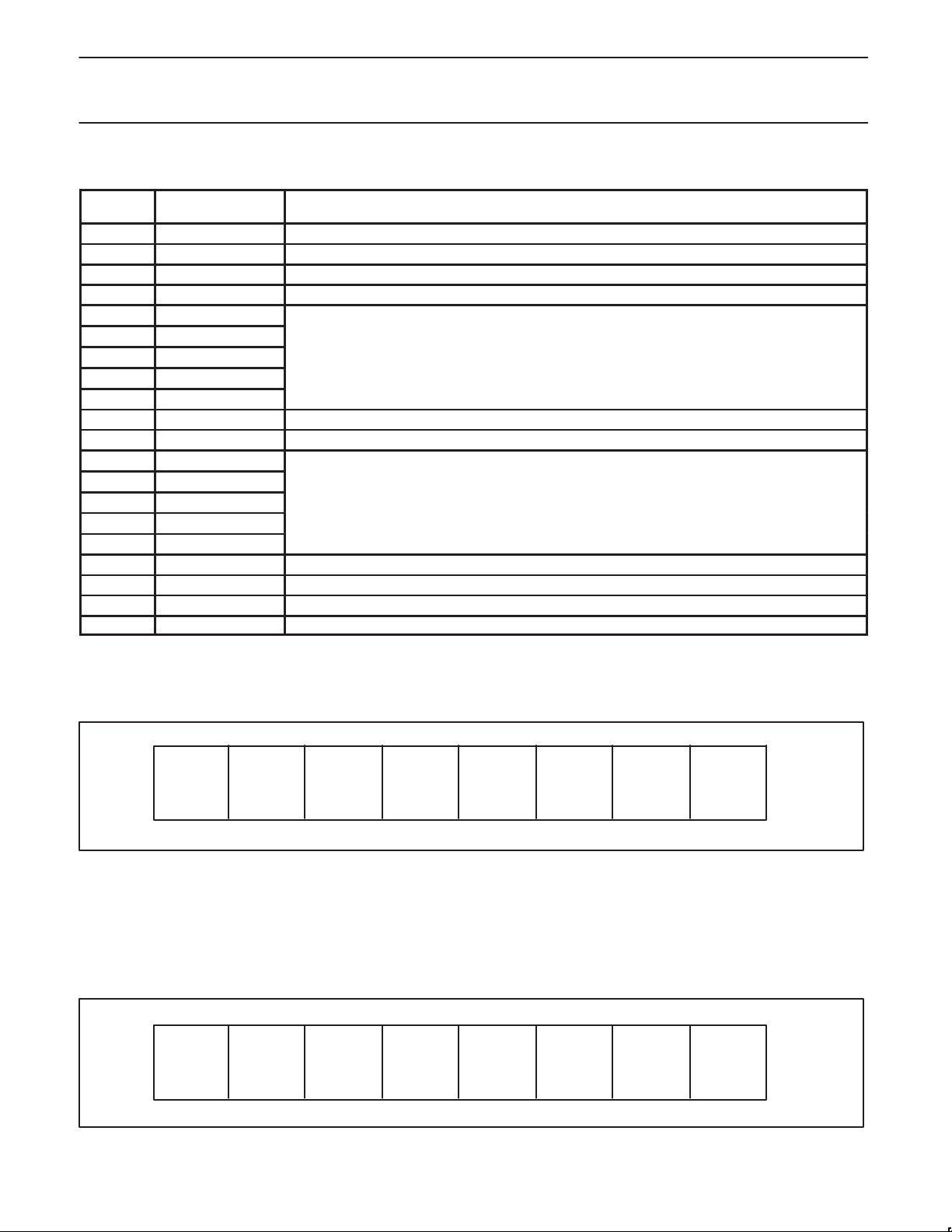
Communicating with this device is initiated by sending a valid address on the I2C bus. The address format (see FIgure 1) has 5 fixed bits and
two user-programmable bits followed by a 1-bit read/write value which determines the direction of the data transfer.
MSB LSB
10 0
1 1 A1 A0
Figure 1. I2C Address Byte
Following the address and acknowledge bit are 8 data bits which, depending on the read/write bit in the address, will read data from or write
data to the non-volatile register . Data will be written to the register if the read/write bit is logic 0 and the WP input is logic 0. Data will be read
from the register if the bit is logic 1. The four high-order bits are latched outputs, while the four low order bits are multiplexed outputs (Figure 2).
NOTE:
1. To ensure data integrity, the non-volatile register must be internally write protected when V
component is dropped below normal operating levels.
MSB LSB
00
Non_muxed
Data
Mux
Data E
Mux
Data D
to the I2C bus is powered down or VCC to the
CC
Mux
Data C
Mux
Data B
R/W#
SW00218
Mux
Data A
SW00456
2000 Jan 31
Figure 2. I2C Data Byte
3
 Loading...