

INTEGRATED CIRCUITS
PCA9557
2
8-bit I
Product data
File under Integrated Circuits — ICL03
C and SMBus I/0 port with reset
2001 Dec 12
Philips Semiconductors Product data
PCA95578-bit I2C and SMBus I/0 port with reset
The system master can also invert the PCA9557 inputs by writing to
the active HIGH polarity inversion register.
Finally, the system master can reset the PCA9557 in the event of a
timeout by asserting a LOW in the reset input.
The power-on reset puts the registers in their default state and
initializes the I
same reset/initialization to occur without depowering the part.
2
C/SMBus state machine. The RESET pin causes the
FEATURES
•Lower voltage, higher performance migration path for the
PCA9556
•8 general purpose input/output expander/collector
•Input/output configuration register
•Active HIGH polarity inversion register
2
•I
C and SMBus interface logic
•Internal power-on reset
•Noise filter on SCL/SDA inputs
•Active LOW reset input
•3 address pins allowing up to 8 devices on the I
2
C/SMBus
•High impedance open drain on I/O0
•No glitch on power-up
•Power-up with all channels configured as inputs
•Low standby current
•Operating power supply voltage range of 2.3 V to 5.5 V
•5 V tolerant inputs/outputs
•0 to 400 kHz clock frequency
•ESD protection exceeds 2000 V HBM per JESD22-A114,
200 V MM per JESD22-A115 and 1000 V CDM per JESD22-C101
•Latch-up testing is done to JESDEC Standard JESD78 which
exceeds 100 mA
•Package offer: SO 16, TSSOP 16
DESCRIPTION
The PCA9557 is a silicon CMOS circuit which provides parallel
input/output expansion for SMBus and I
PCA9557 consists of an 8-bit input port register, 8-bit output port
register, and an I
consumption and a high impedance open drain output pin, I/O0.
The system master can enable the PCA9557’s I/O as either input or
output by writing to the configuration register.
2
C/SMBus interface. It has low current
2
C applications. The
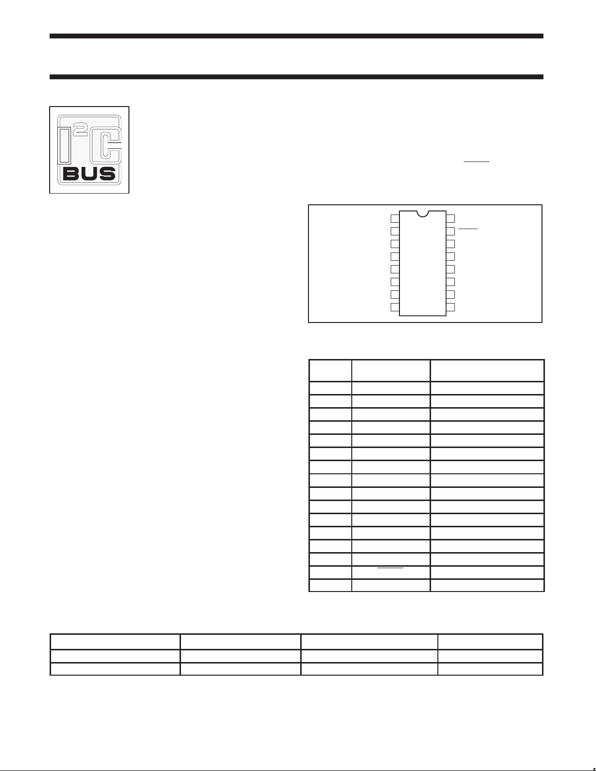
PIN CONFIGURATION
1
SCL
2
SDA
3
A0
A1
4
A2
5
6
I/O0
I/O1
7
V
8
SS
Figure 1. Pin configuration
16
15
14
13
12
11
10
9
V
DD
RESET
I/O7
I/O6
I/O5
I/O4
I/O3
I/O2
PIN DESCRIPTION
PIN
NUMBER
1 SCL Serial clock line
2 SDA Serial data line
3 A0 Address input 0
4 A1 Address input 1
5 A2 Address input 2
6 I/O0 I/O0 (open drain)
7 I/O1 I/O1
8 V
9 I/O2 I/O2
10 I/O3 I/O3
11 I/O4 I/O4
12 I/O5 I/O5
13 I/O6 I/O6
14 I/O7 I/O7
15 RESET Active low reset input
16 V
SYMBOL FUNCTION
SS
DD
Supply ground
Supply voltage
su01045
ORDERING INFORMATION
PACKAGES TEMPERATURE RANGE ORDER CODE DRAWING NUMBER
16-Pin Plastic SO (narrow) –40 to +85 °C PCA9557D SOT109-1
16-Pin Plastic TSSOP –40 to +85 °C PCA9557PW SOT403-1
Standard packing quantities and other packaging data is available at www.philipslogic.com/packaging.
SMBus as specified by the Smart Battery System Implementers Forum is a derivative of the Philips I
2
C is a trademark of Philips Semiconductors Corporation.
I
2001 Dec 12 853-2308 27449
2
2
C patent.

Philips Semiconductors Product data
PCA95578-bit I2C and SMBus I/0 port with reset
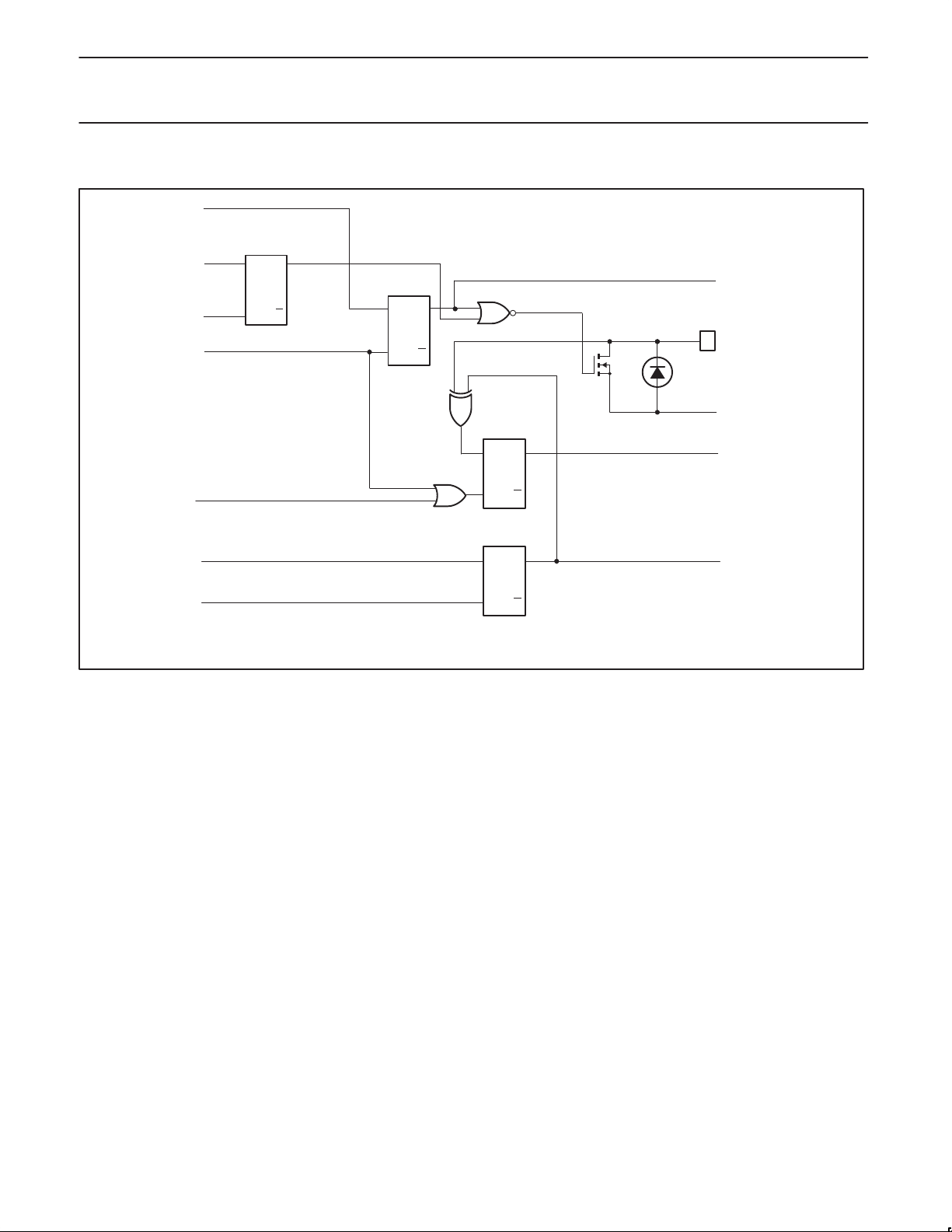
BLOCK DIAGRAM
PCA9557
A0
A1
A2
SCL
SDA
V
DD
V
SS
RESET
SYSTEM DIAGRAM
VCC= 16
GND = 8
15
RESET
1.1 KΩ
INPUT
FILTER
POWER-ON
RESET
I2C/SMBus
CONTROL
8-BIT
WRITE pulse
READ pulse
INPUT/
OUTPUT
PORTS
Figure 2. Block diagram
Input Port Polarity Inversion Configuration Output Port
Q7
Q6
Q5
Q7
Q6
Q5
Q7
Q6
Q5
Q7
Q6
Q5
I/O0
I/O1
I/O2
I/O3
I/O4
I/O5
I/O6
I/O7
I/O0
I/O1
I/O2
SW00827
1.1 KΩ
6
7
9
1
2
A2
5
A1
4
A0
3
2001 Dec 12
SCL
SDA
1.6 KΩ
1.6 KΩ
1.1 KΩ
or
1.1 KΩ
or
1.1 KΩ
or
I2C/SMBus
Interface
logic
Q4
Q3
Q2
Q1
Q0
Q4
Q3
Q2
Q1
Q0
Q4
Q3
Q2
Q1
Q0
Q4
Q3
Q2
Q1
Q0
I/O3
I/O4
I/O5
I/O6
I/O7
10
11
12
13
14
SW00794
Figure 3. System diagram
3
Philips Semiconductors Product data
PCA95578-bit I2C and SMBus I/0 port with reset
SIMPLIFIED SCHEMATIC OF I/O0
DATA FROM
SHIFT REGISTER
CONFIGURATION
DATA FROM
SHIFT REGISTER
WRITE
CONFIGURATION
PULSE
WRITE PULSE
READ PULSE
REGISTER
Q
D
FF
Q
C
K
D
Q
FF
Q
C
K
OUTPUT
PORT
REGISTER
INPUT PORT
REGISTER
D
Q
FF
Q
C
K
OUTPUT PORT
REGISTER DATA
I/O0
ESD PROTECTION DIODE
V
SS
INPUT PORT
REGISTER DATA
DATA FROM
SHIFT REGISTER
WRITE POLARITY
PULSE
NOTE: On power–up or reset, all registers return to default values.
Figure 4. Simplified schematic of I/O0
D
Q
FF
Q
C
K
POLARITY
INVERSION
REGISTER
POLARITY
REGISTER DATA
SW00795
2001 Dec 12
4
Philips Semiconductors Product data
PCA95578-bit I2C and SMBus I/0 port with reset
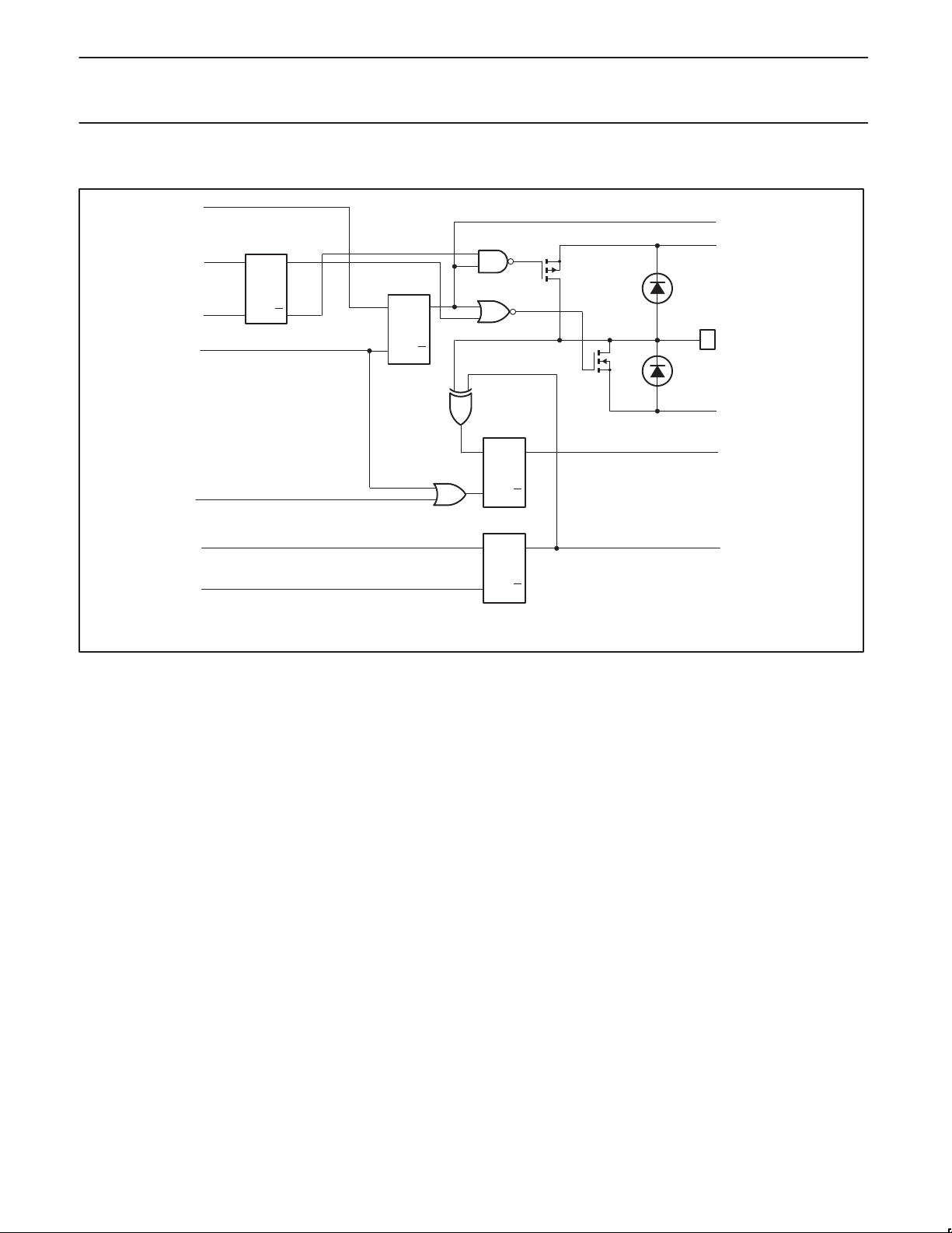
SIMPLIFIED SCHEMATIC OF I/O1 TO I/O7
DATA FROM
SHIFT REGISTER
CONFIGURATION
DATA FROM
SHIFT REGISTER
WRITE
CONFIGURATION
SHIFT REGISTER
WRITE POLARITY
PULSE
WRITE PULSE
READ PULSE
DATA FROM
PULSE
REGISTER
Q
D
FF
Q
C
K
D
Q
FF
Q
C
K
OUTPUT
PORT
REGISTER
NOTE: On power–up or reset, all registers return to default values.
Figure 5. Simplified schematic of I/O1 to I/O7
INPUT PORT
REGISTER
D
Q
FF
Q
C
K
D
Q
FF
Q
C
K
POLARITY
INVERSION
REGISTER
OUTPUT PORT
REGISTER DATA
V
DD
ESD PROTECTION DIODE
I/O1 TO I/O7
ESD PROTECTION DIODE
V
SS
INPUT PORT
REGISTER DATA
POLARITY
REGISTER DATA
SW00796
2001 Dec 12
5
 Loading...