


INTEGRATED CIRCUITS
PCA9556
Octal SMBus Registered Interface
Product specification 1998 Dec 18
Philips Semiconductors Product specification
PCA9556Octal SMBus Registered Interface
FEATURES
•SMBus compliance with fixed 3.3V voltage levels
•Operating power supply voltage range of 3.0V – 3.6V
•Active high polarity inverter register
•Write protect register
•Active low reset pin
•Low leakage current on power-down
•Noise filter on SCL/SDA inputs
•No glitch on power-up
•Internal power-on reset
•8 I/O pins which default to 8 inputs
•High impedance open drain on I/O
DESCRIPTION
The PCA9556 is a silicon CMOS circuit which provides parallel
input/output expansion for SMBus applications. The PCA9556
consists of an 8-bit input port register, 8-bit output port register, and
an SMBus interface. It has low current consumption and a high
impedance open drain output pin, I/O0.
The SMBus system master can reset the PCA9556 in the event of a
timeout by asserting a LOW on the reset input. The SMBus system
master can also invert the PCA9556 inputs by writing to their active
HIGH polarity inversion bits. Finally, the SMBus system master can
enable the PCA9556’s I/Os as either inputs or outputs by writing to
their I/O configuration bits.
The power-on reset sets the registers to their default values and
initializes the SMBus state machine. The RESET
same reset/initialization to occur without depowering the part.
pin causes the
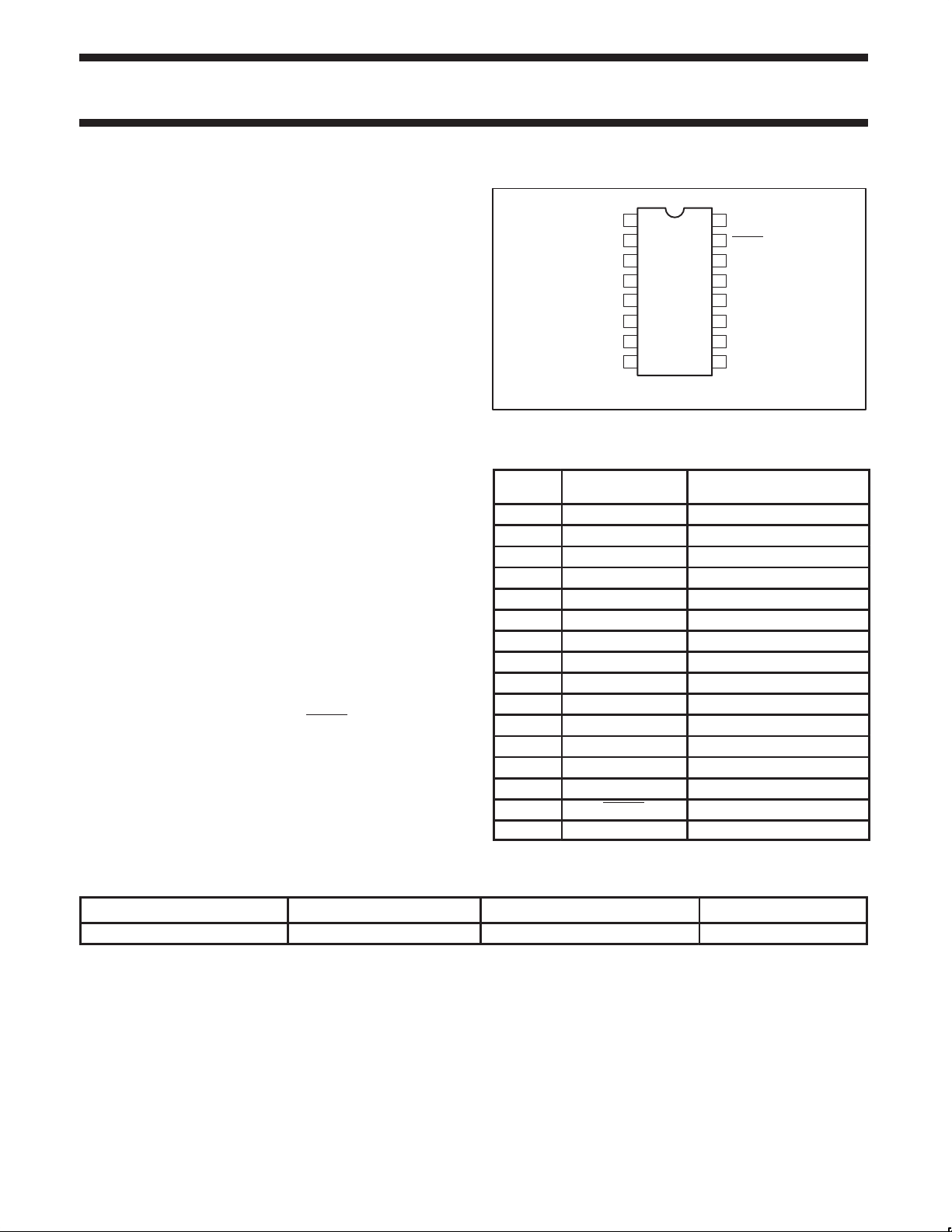
PIN CONFIGURATION
1
SCL
2
SDA
3
A0
A1
4
A2
5
6
I/O0
I/O1
7
V
8
SS
Figure 1. Pin configuration
16
15
14
13
12
11
10
9
su01045
V
DD
RESET
I/O7
I/O6
I/O5
I/O4
I/O3
I/O2
PIN DESCRIPTION
PIN
NUMBER
1 SCL Serial clock line
2 SDA Serial data line
3 A0 Address input 0
4 A1 Address input 1
5 A2 Address input 2
6 I/O0 I/O0 (open drain)
7 I/O1 I/O1
8 V
9 I/O2 I/O2
10 I/O3 I/O3
11 I/O4 I/O4
12 I/O5 I/O5
13 I/O6 I/O6
14 I/O7 I/O7
15 RESET External reset (active LOW)
16 V
SYMBOL FUNCTION
SS
DD
Supply GROUND
Supply voltage
ORDERING INFORMATION
PACKAGES TEMPERATURE RANGE OUTSIDE NORTH AMERICA DRAWING NUMBER
16-Pin Plastic TSSOP16 Type I 0°C to +70°C PCA9556 PW SOT403-1
1998 Dec 18 853-2138 20549
2
Philips Semiconductors Product specification
PCA9556Octal SMBus Registered Interface
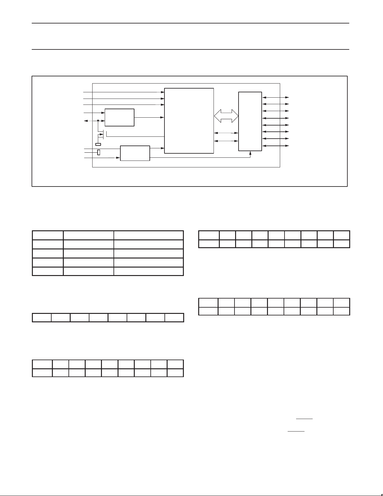
BLOCK DIAGRAM
A0
A1
A2
SCL
SDA
V
V
RESET
DD
SS
INPUT
FILTER
POWER-
ON
RESET
Figure 2. Block diagram
REGISTERS
Command Byte
Command Protocol Function
0 Read byte Input port register
1 Read/write byte Output port register
2 Read/write byte Polarity inversion register
3 Read/write byte I/O configuration register
The command byte is the first byte to follow the address byte during
a write transmission. It is used as a pointer to determine which of the
following registers will be written or read.
Register 0 – Input Port Register
I7 I6 I5 I4 I3 I2 I1 I0
This register is an input-only port. It reflects the incoming logic levels
of the pins, regardless of whether the pin is defined as an input or an
output by register 3. Writes to this register have no effect.
Register 1 – Output Port Register
O7 O6 O5 O4 O3 O2 O1 O0
bit
default 0 0 0 0 0 0 0 0
This register is an output-only port. It reflects the outgoing logic
levels of the pins defined as outputs by register 3. Bit values in this
register have no effect on pins defined as inputs. In turn, reads from
this register reflect the value that is in the flip-flop controlling the
output selection, NOT the actual pin value.
I/O0
I/O1
I/O2
I/O3
I/O4
I/O5
I/O6
I/O7
su01046
SMBUS
CONTROL
8-BIT
WRITE pulse
READ pulse
NOTE: ALL I/Os ARE SET TO INPUTS AT RESET
INPUT/
OUT-
PUT
PORTS
Register 2 – Polarity Inversion Register
bit N7 N6 N5 N4 N3 N2 N1 N0
default 1 1 1 1 0 0 0 0
This register enables polarity inversion of pins defined as inputs by
register 3. If a bit in this register is set (written with ‘1’), the
corresponding port pin’s polarity is inverted. If a bit in this register is
cleared (written with a ‘0’), the corresponding port pin’s original
polarity is retained.
Register 3 – Input/Output Configuration Register
bit C7 C6 C5 C4 C3 C2 C1 C0
default 1 1 1 1 1 1 1 1
This register configures the directions of the I/O pins. If a bit in this
register is set (written with ‘1’), the corresponding port pin is enabled
as an input with high impedance output driver. If a bit in this register
is cleared (written with ‘0’), the corresponding port pin is enabled as
an output.
RESET
Power-on Reset
When power is applied to VDD, an internal power-on reset holds the
PCA9556 in a reset state until V
has reached V
DD
the reset condition is released and the PCA9556 registers and
SMBus state machine will initialize to their default states.
External Reset
A reset can be accomplished by holding the RESET pin low for a
minimum of T
will be held in their default state until the RESET
high. This input contains an internal pull-up, therefore, it may be left
open if not used.
. The PCA9556 registers and SMBus state machine
W
input is once again
. At that point,
POR
1998 Dec 18
3
Philips Semiconductors Product specification
PCA9556Octal SMBus Registered Interface
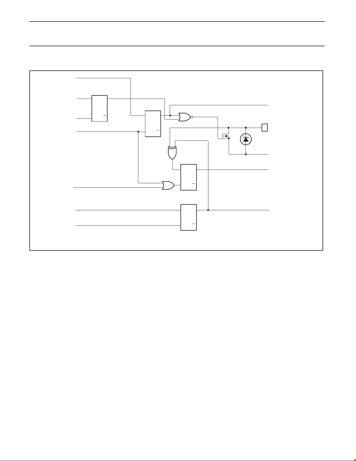
SIMPLIFIED SCHEMATIC OF I/O0
DATA FROM
SHIFT REGISTER
DATA FROM
SHIFT REGISTER
WRITE MASK PULSE
WRITE PULSE
READ PULSE
INPUT/OUTPUT
MASK REGISTER
Q
D
FF
Q
C
K
WRITE
REGISTER
D
Q
FF
Q
C
K
READ
REGISTER
D
Q
FF
Q
C
K
OUTPUT PORT
REGISTER DATA
I/O0
ESD PROTECTION DIODE
V
SS
INPUT PORT
REGISTER DATA
DATA FROM
SHIFT REGISTER
WRITE
POLARITY
PULSE
NOTE: ON POWER-UP OR RESET, ALL REGISTERS RETURN TO DEFAULT VALUES
Figure 3. Simplified schematic of I/O0
POLARITY
REGISTER
D
Q
FF
Q
C
K
POLARITY
REGISTER DATA
su01047
1998 Dec 18
4
 Loading...