

Philips P89C51RA2BA-01, P89C51RA2BBD-01, P89C51RB2BA-01, P89C51RB2BBD-01, P89C51RC2BN-01 User Manual
...
查询P89C51RA2BA/01供应商
INTEGRATED CIRCUITS
P89C51RA2xx/RB2xx/RC2xx/RD2xx
80C51 8-bit Flash microcontroller family
8KB/16KB/32KB/64KB ISP/IAP Flash with
512B/512B/512B/1KB RAM
Preliminary data
Supersedes data of 2002 May 20
2002 Jul 18

Philips Semiconductors Preliminary data
80C51 8-bit Flash microcontroller family
8KB/16KB/32KB/64KB ISP/IAP Flash with 512B/512B/512B/1KB RAM
DESCRIPTION
The P89C51RA2/RB2/RC2/RD2xx contains a non-volatile
8KB/16KB/32KB/64KB Flash program memory that is both parallel
programmable and serial In-System and In-Application
Programmable. In-System Programming (ISP) allows the user to
download new code while the microcontroller sits in the application.
In-Application Programming (IAP) means that the microcontroller
fetches new program code and reprograms itself while in the
system. This allows for remote programming over a modem link.
A default serial loader (boot loader) program in ROM allows serial
In-System programming of the Flash memory via the UART without
the need for a loader in the Flash code. For In-Application
Programming, the user program erases and reprograms the Flash
memory by use of standard routines contained in ROM.
The device supports 6-clock/12-clock mode selection by
programming a Flash bit using parallel programming or
In-System Programming. In addition, an SFR bit (X2) in the clock
control register (CKCON) also selects between 6-clock/12-clock
mode.
Additionally, when in 6-clock mode, peripherals may use either 6
clocks per machine cycle or 12 clocks per machine cycle. This
choice is available individually for each peripheral and is selected by
bits in the CKCON register.
This device is a Single-Chip 8-Bit Microcontroller manufactured in an
advanced CMOS process and is a derivative of the 80C51
microcontroller family . The instruction set is 100% compatible with
the 80C51 instruction set.
The device also has four 8-bit I/O ports, three 16-bit timer/event
counters, a multi-source, four-priority-level, nested interrupt structure,
an enhanced UART and on-chip oscillator and timing circuits.
The added features of the P89C51RA2/RB2/RC2/RD2xx make it a
powerful microcontroller for applications that require pulse width
modulation, high-speed I/O and up/down counting capabilities such
as motor control.
FEA TURES
•80C51 Central Processing Unit
•On-chip Flash Program Memory with In-System Programming
•Boot ROM contains low level Flash programming routines for
•Can be programmed by the end-user application (IAP)
•Parallel programming with 87C51 compatible hardware interface
•Supports 6-clock/12-clock mode via parallel programmer (default
•6-clock/12-clock mode Flash bit erasable and programmable via
•6-clock/12-clock mode programmable “on-the-fly” by SFR bit
•Peripherals (PCA, timers, UART) may use either 6-clock or
•Speed up to 20 MHz with 6-clock cycles per machine cycle
•Fully static operation
•RAM expandable externally to 64 kbytes
•Four interrupt priority levels
•Seven interrupt sources
•Four 8-bit I/O ports
•Full-duplex enhanced UART
•Power control modes
•Programmable clock-out pin
•Second DPTR register
•Asynchronous port reset
•Low EMI (inhibit ALE)
•Programmable Counter Array (PCA)
P89C51RA2/RB2/RC2/RD2xx
(ISP) and In-Application Programming (IAP) capability
downloading via the UART
to programmer
clock mode after ChipErase is 12-clock)
ISP
12-clock mode while the CPU is in 6-clock mode
(40 MHz equivalent performance); up to 33 MHz with 12 clocks
per machine cycle
– Framing error detection
– Automatic address recognition
– Clock can be stopped and resumed
– Idle mode
– Power down mode
– PWM
– Capture/compare
2002 Jul 18
2
Philips Semiconductors Preliminary data
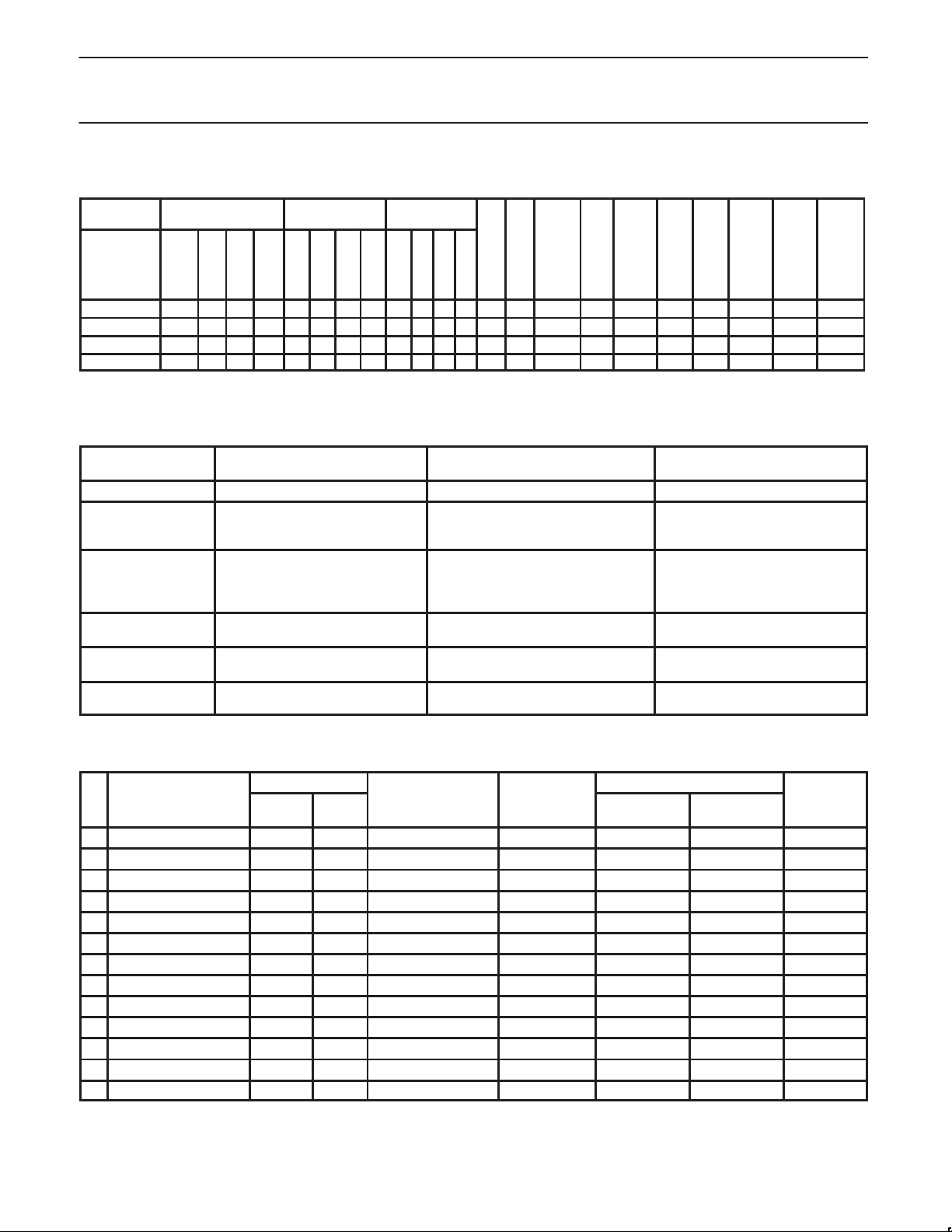
PART ORDER
VOLTAGE
P89C51RA2/RB2/RC2/RD2xx80C51 8-bit Flash microcontroller family
8KB/16KB/32KB/64KB ISP/IAP Flash with 512B/512B/512B/1KB RAM
SELECTION TABLE
WD
Serial
Interfaces
C
2
UART
I
CAN
SPI
ADC bits/ch.
I/O Pins
Interrupts
(Ext.)/Levels
Program
Security
Default Clock
Rate1Optional
Max.
Freq.
at 6-clk
/ 12-clk
Clock Rate1Reset active
(MHz)
low/high?
Freq.
Range
at 3V
(MHz)
Freq.
Range
at 5V
(MHz)
Type Memory Timers
RAM
ROM
OTP
Flash
P89C51RD2xx 1K – – 64K 4 √ √ √ √ – – – – 32 7(2)/4 √ 12-clk 6-clk H 20/33 – 0-20/33
P89C51RC2xx 512B – – 32K 4 √ √ √ √ – – – – 32 7(2)/4 √ 12-clk 6-clk H 20/33 – 0-20/33
P89C51RB2xx 512B – – 16K 4 √ √ √ √ – – – – 32 7(2)/4 √ 12-clk 6-clk H 20/33 – 0-20/33
P89C51RA2xx 512B – – 8K 4 √ √ √ √ – – – – 32 7(2)/4 √ 12-clk 6-clk H 20/33 – 0-20/33
# of Timers
PWM
PCA
NOTE:
1. P89C51Rx2Hxx devices have a 6-clk default clock rate (12-clk optional). Please also see Device Comparison Table.
DEVICE COMPARISON TABLE
Item 1st generation of Rx2 devices 2nd generation of Rx2 devices
(this data sheet)
Type description P89C51Rx2Hxx(x) P89C51Rx2xx(x) No more letter ‘H’
Programming algo-
rithm
Clock mode (I) 6-clk default, OTP configuration bit
Clock mode (II) N/A 6-clock/12-clock mode programmable
Peripheral clock
modes
Flash block structure Two 8-Kbyte blocks
When using a parallel programmer,
be sure to select
P89C51Rx2Hxx(x) devices
When using a parallel programmer, be
sure to select P89C51Rx2xx(x) devices (no more letter ‘H’)
12-clk default, Flash configuration bit
to program to 12-clk mode using
parallel programmer (cannot be
programmed back to 6-clk)
to program to 6-clk mode using paral-
lel programmer or ISP (can be repro-
grammed)
“on the fly” by SFR bit X2 (CKCON.0)
N/A Peripherals can be run in 12-clk mode
while CPU runs in 6-clk mode
2–16 4-Kbyte blocks More flexibility
Different programming algorithm
due to process change
More flexibility for the end user,
more compatibility to older
P89C51Rx+ parts
Clock mode can be changed by
software
More flexibility , lower power consumption
1–3 16-Kbyte blocks
Difference
ORDERING INFORMATION
NUMBER
MEMORY
1
FLASH RAM
TEMPERATURE
RANGE (°C)
AND PACKAGE
RANGE
1. P89C51RA2BA/01 8 KB 512 B 0 to +70, PLCC 4.5–5.5 V 0 to 20 MHz 0 to 33 MHz SOT187-2
2. P89C51RA2BBD/01 8 KB 512 B 0 to +70, LQFP 4.5–5.5 V 0 to 20 MHz 0 to 33 MHz SOT389-1
3. P89C51RB2BA/01 16 KB 512 B 0 to +70, PLCC 4.5–5.5 V 0 to 20 MHz 0 to 33 MHz SOT187-2
4. P89C51RB2BBD/01 16 KB 512 B 0 to +70, LQFP 4.5–5.5 V 0 to 20 MHz 0 to 33 MHz SOT389-1
5. P89C51RC2BN/01 32 KB 512 B 0 to +70, PDIP 4.5–5.5 V 0 to 20 MHz 0 to 33 MHz SOT129-1
6. P89C51RC2BA/01 32 KB 512 B 0 to +70, PLCC 4.5–5.5 V 0 to 20 MHz 0 to 33 MHz SOT187-2
7. P89C51RC2FA/01 32 KB 512 B –40 to +85, PLCC 4.5–5.5 V 0 to 20 MHz 0 to 33 MHz SOT187-2
8. P89C51RC2BBD/01 32 KB 512 B 0 to +70, LQFP 4.5–5.5 V 0 to 20 MHz 0 to 33 MHz SOT389-1
9. P89C51RC2FBD/01 32 KB 512 B –40 to +85, LQFP 4.5–5.5 V 0 to 20 MHz 0 to 33 MHz SOT389-1
10. P89C51RD2BN/01 64 KB 1024 B 0 to +70, PDIP 4.5–5.5 V 0 to 20 MHz 0 to 33 MHz SOT129-1
11. P89C51RD2BA/01 64 KB 1024 B 0 to +70, PLCC 4.5–5.5 V 0 to 20 MHz 0 to 33 MHz SOT187-2
12. P89C51RD2BBD/01 64 KB 1024 B 0 to +70, LQFP 4.5–5.5 V 0 to 20 MHz 0 to 33 MHz SOT389-1
13. P89C51RD2FA/01 64 KB 1024 B –40 to +85, PLCC 4.5–5.5 V 0 to 20 MHz 0 to 33 MHz SOT187-2
NOTE:
1. The Part Marking will not include the “/01”.
2002 Jul 18
3
FREQUENCY (MHz)
6-CLOCK
MODE
12-CLOCK
MODE
DWG #
Philips Semiconductors Preliminary data
P89C51RA2/RB2/RC2/RD2xx80C51 8-bit Flash microcontroller family
8KB/16KB/32KB/64KB ISP/IAP Flash with 512B/512B/512B/1KB RAM
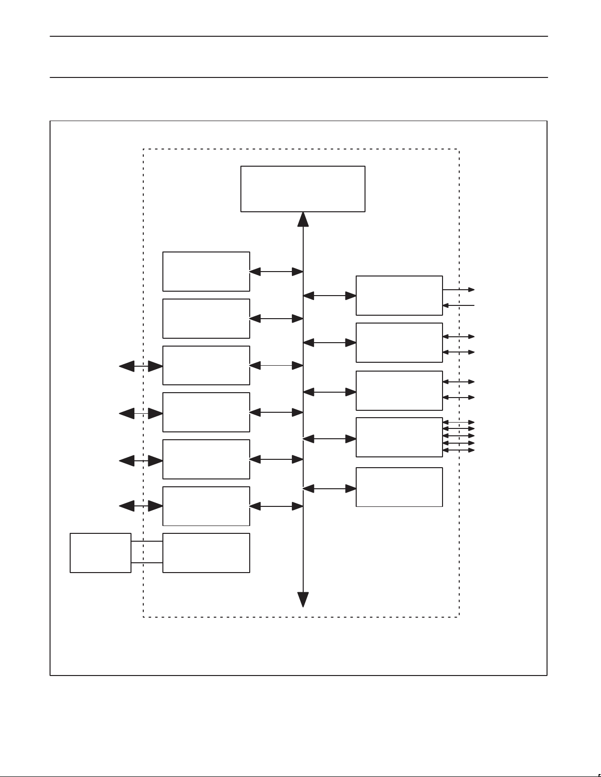
BLOCK DIAGRAM 1
ACCELERATED 80C51 CPU
(12-CLK MODE, 6-CLK MODE)
8K / 16K / 32K /
64 KBYTE
CODE FLASH
FULL-DUPLEX
ENHANCED UART
512 / 1024 BYTE
DATA RAM
TIMER 0
TIMER 1
PORT 3
CONFIGURABLE I/Os
TIMER 2
RESONATOR
PORT 2
CONFIGURABLE I/Os
PORT 1
CONFIGURABLE I/Os
PORT 0
CONFIGURABLE I/Os
OSCILLATORCRYSTAL OR
PROGRAMMABLE
COUNTER ARRAY
(PCA)
WATCHDOG TIMER
su01606
2002 Jul 18
4

Philips Semiconductors Preliminary data
P89C51RA2/RB2/RC2/RD2xx80C51 8-bit Flash microcontroller family
8KB/16KB/32KB/64KB ISP/IAP Flash with 512B/512B/512B/1KB RAM
BLOCK DIAGRAM – CPU ORIENTED
P0.0–P0.7 P2.0–P2.7
PSEN
EAV
ALE
RST
PORT 0
DRIVERS
V
CC
V
SS
RAM ADDR
REGISTER
B
REGISTER
TIMING
PP
AND
CONTROL
INSTRUCTION
PD
REGISTER
RAM
ACC
TMP2
PSW
PORT 1
LATCH
PORT 0
LATCH
ALU
TMP1
PORT 2
DRIVERS
PORT 2
LATCH
SFRs
TIMERS
P.C.A.
STACK
POINTER
PORT 3
LATCH
FLASH
PROGRAM
ADDRESS
REGISTER
BUFFER
PC
INCRE-
MENTER
8 16
PROGRAM
COUNTER
DPTR’S
MULTIPLE
8
2002 Jul 18
OSCILLATOR
XTAL1 XTAL2
PORT 1
DRIVERS
P1.0–P1.7
PORT 3
DRIVERS
P3.0–P3.7
SU01065
5

Philips Semiconductors Preliminary data
P89C51RA2/RB2/RC2/RD2xx80C51 8-bit Flash microcontroller family
8KB/16KB/32KB/64KB ISP/IAP Flash with 512B/512B/512B/1KB RAM
LOGIC SYMBOL
V
V
SS
CC
XTAL1
XTAL2
RST
EA/V
PP
PSEN
ALE/PROG
RxD
TxD
INT0
INT1
T0
PORT 3
T1
WR
RD
SECONDARY FUNCTIONS
PINNING
Plastic Dual In-Line Package
T2/P1.0
1
T2EX/P1.1
CEX0/P1.3
CEX1/P1.4
CEX2/P1.5
CEX3/P1.6
CEX4/P1.7
INT0
INT1
ECI/P1.2
RST
RxD/P3.0
TxD/P3.1
/P3.2
/P3.3
T0/P3.4
T1/P3.5
/P3.6
WR
/P3.7
RD
XTAL2
XTAL1
V
SS
2
3
4
5
6
7
8
9
10
11
12
13
14
15
16
17
18
19
20
DUAL
IN-LINE
PACKAGE
PORT 0
PORT 1PORT 2
V
40
P0.0/AD0
39
38
P0.1/AD1
37
P0.2/AD2
36
P0.3/AD3
35
P0.4/AD4
34
P0.5/AD5
33
P0.6/AD6
32
P0.7/AD7
31
EA/V
30
ALE/PROG
29
PSEN
28
P2.7/A15
27
P2.6/A14
26
P2.5/A13
25
P2.4/A12
24
P2.3/A11
23
P2.2/A10
22
P2.1/A9
21
P2.0/A8
ADDRESS AND
DATA BUS
T2
T2EX
ADDRESS BUS
CC
PP
SU00021
SU01302
Plastic Leaded Chip Carrier
6140
7
LCC
17
18 28
Pin Function
1 NIC*
2 P1.0/T2
3 P1.1/T2EX
4 P1.2/ECI
5 P1.3/CEX0
6 P1.4/CEX1
7 P1.5/CEX2
8 P1.6/CEX3
9 P1.7/CEX4
10 RST
11 P3.0/RxD
12 NIC*
13 P3.1/TxD
14 P3.2/INT0
15 P3.3/INT1
* NO INTERNAL CONNECTION
Pin Function
16 P3.4/T0
17 P3.5/T1
18 P3.6/WR
19 P3.7/RD
20 XTAL2
21 XTAL1
22 V
SS
23 NIC*
24 P2.0/A8
25 P2.1/A9
26 P2.2/A10
27 P2.3/A11
28 P2.4/A12
29 P2.5/A13
30 P2.6/A14
Plastic Quad Flat Pack
44 34
1
LQFP
11
12 22
Pin Function
1 P1.5/CEX2
2 P1.6/CEX3
3 P1.7/CEX4
4 RST
5 P3.0/RxD
6 NIC*
7 P3.1/TxD
8 P3.2/INT0
9 P3.3/INT1
10 P3.4/T0
11 P3.5/T1
12 P3.6/WR
13 P3.7/RD
14 XTAL2
15 XTAL1
* NO INTERNAL CONNECTION
Pin Function
16 V
SS
17 NIC*
18 P2.0/A8
19 P2.1/A9
20 P2.2/A10
21 P2.3/A11
22 P2.4/A12
23 P2.5/A13
24 P2.6/A14
25 P2.7/A15
26 PSEN
27 ALE/PROG
28 NIC*
29 EA
/V
30 P0.7/AD7
39
29
Pin Function
31 P2.7/A15
32 PSEN
33 ALE/PROG
34 NIC*
35 EA/V
36 P0.7/AD7
37 P0.6/AD6
38 P0.5/AD5
39 P0.4/AD4
40 P0.3/AD3
41 P0.2/AD2
42 P0.1/AD1
43 P0.0/AD0
44 V
PP
CC
SU00023
33
23
Pin Function
31 P0.6/AD6
32 P0.5/AD5
33 P0.4/AD4
34 P0.3/AD3
35 P0.2/AD2
36 P0.1/AD1
37 P0.0/AD0
38 V
CC
39 NIC*
40 P1.0/T2
41 P1.1/T2EX
42 P1.2/ECI
43 P1.3/CEX0
PP
44 P1.4/CEX1
SU01400
2002 Jul 18
6
Philips Semiconductors Preliminary data
MNEMONIC
TYPE
NAME AND FUNCTION
P89C51RA2/RB2/RC2/RD2xx80C51 8-bit Flash microcontroller family
8KB/16KB/32KB/64KB ISP/IAP Flash with 512B/512B/512B/1KB RAM
PIN DESCRIPTIONS
PIN NUMBER
PDIP PLCC LQFP
V
SS
V
CC
P0.0–0.7 39–32 43–36 37–30 I/O Port 0: Port 0 is an open-drain, bidirectional I/O port. Port 0 pins that have 1s
P1.0–P1.7 1–8 2–9 40–44,
P2.0–P2.7 21–28 24–31 18–25 I/O Port 2: Port 2 is an 8-bit bidirectional I/O port with internal pull-ups. Port 2 pins that
P3.0–P3.7 10–17 11,
RST 9 10 4 I Reset: A high on this pin for two machine cycles while the oscillator is running,
ALE 30 33 27 O Address Latch Enable: Output pulse for latching the low byte of the address
20 22 16 I Ground: 0 V reference.
40 44 38 I Power Supply: This is the power supply voltage for normal, idle, and power-down
operation.
written to them float and can be used as high-impedance inputs. Port 0 is also the
multiplexed low-order address and data bus during accesses to external program
and data memory. In this application, it uses strong internal pull-ups when emitting 1s.
I/O Port 1: Port 1 is an 8-bit bidirectional I/O port with internal pull-ups on all pins.
1–3
Port 1 pins that have 1s written to them are pulled high by the internal pull-ups and
can be used as inputs. As inputs, port 1 pins that are externally pulled low will
source current because of the internal pull-ups. (See DC Electrical Characteristics:
).
I
IL
Alternate functions for P89C51RA2/RB2/RC2/RD2xx Port 1 include:
1 2 40 I/O T2 (P1.0): Timer/Counter 2 external count input/Clockout (see Programmable
Clock-Out)
2 3 41 I T2EX (P1.1): Timer/Counter 2 Reload/Capture/Direction Control
3 4 42 I ECI (P1.2): External Clock Input to the PCA
4 5 43 I/O CEX0 (P1.3): Capture/Compare External I/O for PCA module 0
5 6 44 I/O CEX1 (P1.4): Capture/Compare External I/O for PCA module 1
6 7 1 I/O CEX2 (P1.5): Capture/Compare External I/O for PCA module 2
7 8 2 I/O CEX3 (P1.6): Capture/Compare External I/O for PCA module 3
8 9 3 I/O CEX4 (P1.7): Capture/Compare External I/O for PCA module 4
have 1s written to them are pulled high by the internal pull-ups and can be used as
inputs. As inputs, port 2 pins that are externally being pulled low will source current
because of the internal pull-ups. (See DC Electrical Characteristics: I
emits the high-order address byte during fetches from external program memory
). Port 2
IL
and during accesses to external data memory that use 16-bit addresses (MOVX
@DPTR). In this application, it uses strong internal pull-ups when emitting 1s.
During accesses to ext ernal data memory that use 8 -bit addres ses (MOV @Ri),
port 2 emits the contents of the P2 special function register.
5, 7–13 I/O Port 3: Port 3 is an 8-bit bidirectional I/O port with internal pull-ups. Port 3 pins that
13–19
have 1s written to them are pulled high by the internal pull-ups and can be used as
inputs. As inputs, port 3 pins that are externally being pulled low will source current
because of the pull-ups. (See DC Electrical Characteristics: I
the special features of the P89C51RA2/RB2/RC2/RD2xx, as listed below:
). Port 3 also serves
IL
10 11 5 I RxD (P3.0): Serial input port
11 13 7 O TxD (P3.1): Serial output port
12 14 8 I INT0 (P3.2): External interrupt
13 15 9 I INT1 (P3.3): External interrupt
14 16 10 I T0 (P3.4): Timer 0 external input
15 17 11 I T1 (P3.5): Timer 1 external input
16 18 12 O WR (P3.6): External data memory write strobe
17 19 13 O RD (P3.7): External data memory read strobe
resets the device. An internal resistor to V
an external capacitor to V
CC
.
permits a power-on reset using only
SS
during an access to external memory. In normal operation, ALE is emitted twice
every machine cycle, and can be used for external timing or clocking. Note that one
ALE pulse is skipped during each access to external data memory. ALE can be
disabled by setting SFR auxiliary.0. With this bit set, ALE will be active only during a
MOVX instruction.
2002 Jul 18
7

Philips Semiconductors Preliminary data
P89C51RA2/RB2/RC2/RD2xx80C51 8-bit Flash microcontroller family
8KB/16KB/32KB/64KB ISP/IAP Flash with 512B/512B/512B/1KB RAM
MNEMONIC NAME AND FUNCTIONTYPE
MNEMONIC NAME AND FUNCTIONTYPE
PSEN 29 32 26 O Program Store Enable: The read strobe to external program memory. When
EA/V
PP
XTAL1 19 21 15 I Crystal 1: Input to the inverting oscillator amplifier and input to the internal clock
XTAL2 18 20 14 O Crystal 2: Output from the inverting oscillator amplifier.
NOTE:
To avoid “latch-up” effect at power-on, the voltage on any pin (other than V
PIN NUMBER
LQFPPLCCPDIP
executing code from the external program memory, PSEN
machine cycle, except that two PSEN
to external data memory. PSEN
program memory.
31 35 29 I External Access Enable/Programming Supply V oltage: EA must be externally
held low to enable the device to fetch code from external program memory
locations. If EA
The value on the EA
changes have no effect. This pin also receives the programming supply voltage
) during Flash programming.
(V
PP
generator circuits.
is held high, the device executes from internal program memory.
pin is latched when RST is released and any subsequent
) must not be higher than VCC + 0.5 V or less than VSS – 0.5 V.
PP
activations are skipped during each access
is not activated during fetches from internal
is activated twice each
2002 Jul 18
8
Philips Semiconductors Preliminary data
P89C51RA2/RB2/RC2/RD2xx80C51 8-bit Flash microcontroller family
8KB/16KB/32KB/64KB ISP/IAP Flash with 512B/512B/512B/1KB RAM
Table 1. Special Function Registers
SYMBOL DESCRIPTION
ACC* Accumulator E0H E7 E6 E5 E4 E3 E2 E1 E0 00H
AUXR# Auxiliary 8EH – – – – – –
AUXR1# Auxiliary 1 A2H – –
B* B register F0H F7 F6 F5 F4 F3 F2 F1 F0 00H
CCAP0H# Module 0 Capture High FAH xxxxxxxxB
CCAP1H# Module 1 Capture High FBH xxxxxxxxB
CCAP2H# Module 2 Capture High FCH xxxxxxxxB
CCAP3H# Module 3 Capture High FDH xxxxxxxxB
CCAP4H# Module 4 Capture High FEH xxxxxxxxB
CCAP0L# Module 0 Capture Low EAH xxxxxxxxB
CCAP1L# Module 1 Capture Low EBH xxxxxxxxB
CCAP2L# Module 2 Capture Low ECH xxxxxxxxB
CCAP3L# Module 3 Capture Low EDH xxxxxxxxB
CCAP4L# Module 4 Capture Low EEH xxxxxxxxB
CCAPM0# Module 0 Mode DAH – ECOM CAPP CAPN MAT TOG PWM ECCF x0000000B
CCAPM1# Module 1 Mode DBH – ECOM CAPP CAPN MAT TOG PWM ECCF x0000000B
CCAPM2# Module 2 Mode DCH – ECOM CAPP CAPN MAT TOG PWM ECCF x0000000B
CCAPM3# Module 3 Mode DDH – ECOM CAPP CAPN MAT TOG PWM ECCF x0000000B
CCAPM4# Module 4 Mode DEH – ECOM CAPP CAPN MAT TOG PWM ECCF x0000000B
CCON*# PCA Counter Control D8H CF CR – CCF4 CCF3 CCF2 CCF1 CCF0 00x00000B
CH# PCA Counter High F9H 00H
CKCON# Clock control 8FH – WDX2 PCAX2 SIX2 T2X2 T1X2 T0X2 X2 x0000000B
CL# PCA Counter Low E9H 00H
CMOD# PCA Counter Mode D9H CIDL WDTE – – – CPS1 CPS0 ECF 00xxx000B
DPTR: Data Pointer (2 bytes)
DPH Data Pointer High 83H 00H
DPL Data Pointer Low 82H 00H
IE* Interrupt Enable 0 A8H EA EC ET2 ES ET1 EX1 ET0 EX0 00H
IP* Interrupt Priority B8H – PPC PT2 PS PT1 PX1 PT0 PX0 x0000000B
IPH# Interrupt Priority High B7H – PPCH PT2H PSH PT1H PX1H PT0H PX0H x0000000B
DIRECT
ADDRESS
BIT ADDRESS, SYMBOL, OR ALTERNATIVE PORT FUNCTION
MSB LSB
EXTRAM
ENBOOT
DF DE DD DC DB DA D9 D8
AF AE AD AC AB AA A9 A8
BF BE BD BC BB BA B9 B8
– GF2 0 – DPS xxxxxxx0B
AO xxxxxx00B
RESET
VALUE
87 86 85 84 83 82 81 80
P0* Port 0 80H AD7 AD6 AD5 AD4 AD3 AD2 AD1 AD0 FFH
97 96 95 94 93 92 91 90
P1* Port 1 90H CEX4 CEX3 CEX2 CEX1 CEX0 ECI T2EX T2 FFH
A7 A6 A5 A4 A3 A2 A1 A0
P2* Port 2 A0H AD15 AD14 AD13 AD12 AD11 AD10 AD9 AD8 FFH
B7 B6 B5 B4 B3 B2 B1 B0
P3* Port 3 B0H RD WR T1 T0 INT1 INT0 TxD RxD FFH
PCON#1Power Control 87H SMOD1 SMOD0 – POF GF1 GF0 PD IDL 00xxx000B
* SFRs are bit addressable.
# SFRs are modified from or added to the 80C51 SFRs.
– Reserved bits.
1. Reset value depends on reset source.
2002 Jul 18
9
Philips Semiconductors Preliminary data
P89C51RA2/RB2/RC2/RD2xx80C51 8-bit Flash microcontroller family
8KB/16KB/32KB/64KB ISP/IAP Flash with 512B/512B/512B/1KB RAM
Table 1. Special Function Registers (Continued)
SYMBOL DESCRIPTION
PSW* Program Status Word D0H CY AC F0 RS1 RS0 OV F1 P 00000000B
RCAP2H# Timer 2 Capture High CBH 00H
RCAP2L# Timer 2 Capture Low CAH 00H
SADDR# Slave Address A9H 00H
SADEN# Slave Address Mask B9H 00H
SBUF Serial Data Buffer 99H xxxxxxxxB
SCON* Serial Control 98H
SP Stack Pointer 81H 07H
TCON* Timer Control 88H TF1 TR1 TF0 TR0 IE1 IT1 IE0 IT0 00H
DIRECT
ADDRESS
BIT ADDRESS, SYMBOL, OR ALTERNATIVE PORT FUNCTION
MSB LSB
D7 D6 D5 D4 D3 D2 D1 D0
9F 9E 9D 9C 9B 9A 99 98
SM0/FE
8F 8E 8D 8C 8B 8A 89 88
SM1 SM2 REN TB8 RB8 TI RI 00H
RESET
VALUE
CF CE CD CC CB CA C9 C8
T2CON* Timer 2 Control C8H TF2 EXF2 RCLK TCLK EXEN2 TR2 C/T2 CP/RL2 00H
T2MOD# Timer 2 Mode Control C9H – – – – – – T2OE DCEN xxxxxx00B
TH0 Timer High 0 8CH 00H
TH1 Timer High 1 8DH 00H
TH2# T imer High 2 CDH 00H
TL0 Timer Low 0 8AH 00H
TL1 Timer Low 1 8BH 00H
TL2# Timer Low 2 CCH 00H
TMOD Timer Mode 89H GATE C/T M1 M0 GATE C/T M1 M0 00H
WDTRST W atchdog Timer Reset A6H
* SFRs are bit addressable.
# SFRs are modified from or added to the 80C51 SFRs.
– Reserved bits.
OSCILLA T OR CHARACTERISTICS
XTAL1 and XTAL2 are the input and output, respectively, of an
inverting amplifier. The pins can be configured for use as an
on-chip oscillator.
To drive the device from an external clock source, XTAL1 should be
driven while XTAL2 is left unconnected. Minimum and maximum
high and low times specified in the data sheet must be observed.
This device is configured at the factory to operate using 12 clock
periods per machine cycle, referred to in this datasheet as “12-clock
mode”. It may be optionally configured on commercially available
Flash programming equipment or via ISP or via software to operate
at 6 clocks per machine cycle, referred to in this datasheet as
“6-clock mode”. (This yields performance equivalent to twice that of
standard 80C51 family devices). Also see next page.
2002 Jul 18
10
Philips Semiconductors Preliminary data
P89C51RA2/RB2/RC2/RD2xx80C51 8-bit Flash microcontroller family
8KB/16KB/32KB/64KB ISP/IAP Flash with 512B/512B/512B/1KB RAM
CLOCK CONTROL REGISTER (CKCON)
This device provides control of the 6-clock/12-clock mode by means
of both an SFR bit (X2) and a Flash bit (FX2, located in the Security
Block). The Flash clock control bit, FX2, when programmed (6-clock
mode) supercedes the X2 bit (CKCON.0).
CKCON Address = 8Fh Reset Value = x0000000B
Not Bit Addressable
76543210
BIT SYMBOL FUNCTION
CKCON.7 – Reserved.
CKCON.6 WDX2 Watchdog clock; 0 = 6 clocks for each WDT clock, 1 = 12 clocks for each WDT clock
CKCON.5 PCAX2 PCA clock; 0 = 6 clocks for each PCA clock, 1 = 12 clocks for each PCA clock
CKCON.4 SIX2 UART clock; 0 = 6 clocks for each UART clock, 1 = 12 clocks for each UART clock
CKCON.3 T2X2 Timer2 clock; 0 = 6 clocks for each Timer2 clock, 1 = 12 clocks for each Timer2 clock
CKCON.2 T1X2 Timer1 clock; 0 = 6 clocks for each Timer1 clock, 1 = 12 clocks for each Timer1 clock
CKCON.1 T0X2 Timer0 clock; 0 = 6 clocks for each Timer0 clock, 1 = 12 clocks for each Timer0 clock
CKCON.0 X2 CPU clock; 1 = 6 clocks for each machine cycle, 0 = 12 clocks for each machine cycle
The CKCON register also provides individual control of the clock
rates for the peripherals devices. When running in 6-clock mode
each peripheral may be individually clocked from either fosc/6 or
fosc/12. When in 12-clock mode, all peripheral devices will use
fosc/12. The CKCON register is shown below.
T0X2T1X2T2X2SIX2PCAX2WDX2–
X2
SU01607
Bits 1 through 6 only apply if 6 clocks per machine cycle is chosen
(i.e.– Bit 0 = 1). If Bit 0 = 0 (12 clocks per machine cycle) then all
peripherals will have 12 clocks per machine cycle as their clock
source.
FX2 clock mode bit
erased 0 x 12-clock (default) 12-clock (default)
erased 1 0 6-clock 6-clock
erased 1 1 6-clock 12-clock
programmed x 0 6-clock 6-clock
programmed x 1 6-clock 12-clock
X2 Peripheral clock
mode bit
(e.g., T0X2)
Also please note that the clock divider applies to the serial port for
modes 0 & 2 (fixed baud rate modes). This is because modes 1 & 3
(variable baud rate modes) use either Timer 1 or Timer 2.
Below is the truth table for the peripheral input clock sources.
CPU MODE Peripheral Clock Rate
RESET
A reset is accomplished by holding the RST pin high for at least two
machine cycles (12 oscillator periods in 6-clock mode, or 24 oscillator
periods in 12-clock mode), while the oscillator is running. To ensure a
good power-on reset, the RST pin mu st be h i gh l o n g enough to allow
the oscillator time to start up (normally a few milliseconds) plus two
machine cycles. At power-on, the voltage on V
come up at the same time for a proper start-up. Ports 1, 2, and 3 will
asynchronously be driven to their reset condition when a voltage
above V
The value on the EA
no further effect.
(min.) is applied to RST.
IH1
pin is latched when RST is deasserted and has
and RST must
CC
2002 Jul 18
11

Philips Semiconductors Preliminary data
P89C51RA2/RB2/RC2/RD2xx80C51 8-bit Flash microcontroller family
8KB/16KB/32KB/64KB ISP/IAP Flash with 512B/512B/512B/1KB RAM
LOW POWER MODES
Stop Clock Mode
The static design enables the clock speed to be reduced down to
0 MHz (stopped). When the oscillator is stopped, the RAM and
Special Function Registers retain their values. This mode allows
step-by-step utilization and permits reduced system power
consumption by lowering the clock frequency down to any value. For
lowest power consumption the Power Down mode is suggested.
Idle Mode
In the idle mode (see Table 2), the CPU puts itself to sleep while all
of the on-chip peripherals stay active. The instruction to invoke the
idle mode is the last instruction executed in the normal operating
mode before the idle mode is activated. The CPU contents, the
on-chip RAM, and all of the special function registers remain intact
during this mode. The idle mode can be terminated either by any
enabled interrupt (at which time the process is picked up at the
interrupt service routine and continued), or by a hardware reset
which starts the processor in the same manner as a power-on reset.
Power-Down Mode
To save even more power, a Power Down mode (see Table 2) can
be invoked by software. In this mode, the oscillator is stopped and
the instruction that invoked Power Down is the last instruction
executed. The on-chip RAM and Special Function Registers retain
their values down to 2 V and care must be taken to return V
minimum specified operating voltages before the Power Down Mode
is terminated.
Either a hardware reset or external interrupt can be used to exit from
Power Down. Reset redefines all the SFRs but does not change the
on-chip RAM. An external interrupt allows both the SFRs and the
on-chip RAM to retain their values.
To properly terminate Power Down, the reset or external interrupt
should not be executed before V
operating level and must be held active long enough for the
oscillator to restart and stabilize (normally less than 10 ms).
With an external interrupt, INT0 and INT1 must be enabled and
configured as level-sensitive. Holding the pin low restarts the oscillator
but bringing the pin back high completes the exit. Once the interrupt
is serviced, the next instruction to be executed after RETI will be the
one following the instruction that put the device into Power Down.
is restored to its normal
CC
CC
to the
POWER-ON FLAG
The Power-On Flag (POF) is set by on-chip circuitry when the V
level on the P89C51RA2/RB2/RC2/RD2xx rises from 0 to 5 V . The
POF bit can be set or cleared by software allowing a user to
determine if the reset is the result of a power-on or a warm start
after powerdown. The V
to remain unaffected by the V
level must remain above 3 V for the POF
CC
level.
CC
CC
Design Consideration
When the idle mode is terminated by a hardware reset, the device
normally resumes program execution, from where it left off, up to
two machine cycles before the internal reset algorithm takes control.
On-chip hardware inhibits access to internal RAM in this event, but
access to the port pins is not inhibited. To eliminate the possibility of
an unexpected write when Idle is terminated by reset, the instruction
following the one that invokes Idle should not be one that writes to a
port pin or to external memory.
ONCE Mode
The ONCE (“On-Circuit Emulation”) Mode facilitates testing and
debugging of systems without the device having to be removed from
the circuit. The ONCE Mode is invoked by:
1. Pull ALE low while the device is in reset and PSEN is high;
2. Hold ALE low as RST is deactivated.
While the device is in ONCE Mode, the Port 0 pins go into a float
state, and the other port pins and ALE and PSEN
high. The oscillator circuit remains active. While the device is in this
mode, an emulator or test CPU can be used to drive the circuit.
Normal operation is restored when a normal reset is applied.
are weakly pulled
Programmable Clock-Out
A 50% duty cycle clock can be programmed to come out on P1.0.
This pin, besides being a regular I/O pin, has two alternate
functions. It can be programmed:
1. to input the external clock for Timer/Counter 2, or
2. to output a 50% duty cycle clock ranging from 61 Hz to 4 MHz at a
16 MHz operating frequency in 12-clock mode (122 Hz to 8 MHz in
6-clock mode).
To configure the Timer/Counter 2 as a clock generator, bit C/T
T2CON) must be cleared and bit T20E in T2MOD must be set. Bit
TR2 (T2CON.2) also must be set to start the timer.
The Clock-Out frequency depends on the oscillator frequency and
the reload value of Timer 2 capture registers (RCAP2H, RCAP2L)
as shown in this equation:
Oscillator Frequency
n (65536 * RCAP2H, RCAP2L)
n = 2 in 6-clock mode
Where (RCAP2H,RCAP2L) = the content of RCAP2H and RCAP2L
taken as a 16-bit unsigned integer.
In the Clock-Out mode Timer 2 roll-overs will not generate an
interrupt. This is similar to when it is used as a baud-rate generator.
It is possible to use Timer 2 as a baud-rate generator and a clock
generator simultaneously. Note, however, that the baud-rate and the
Clock-Out frequency will be the same.
4 in 12-clock mode
2 (in
Table 2. External Pin Status During Idle and Power-Down Mode
MODE PROGRAM MEMOR Y ALE PSEN PORT 0 PORT 1 PORT 2 PORT 3
Idle Internal 1 1 Data Data Data Data
Idle External 1 1 Float Data Address Data
Power-down Internal 0 0 Data Data Data Data
Power-down External 0 0 Float Data Data Data
2002 Jul 18
12

Philips Semiconductors Preliminary data
P89C51RA2/RB2/RC2/RD2xx80C51 8-bit Flash microcontroller family
8KB/16KB/32KB/64KB ISP/IAP Flash with 512B/512B/512B/1KB RAM
TIMER 0 AND TIMER 1 OPERATION
Timer 0 and Timer 1
The “Timer” or “Counter” function is selected by control bits C/T in
the Special Function Register TMOD. These two Timer/Counters
have four operating modes, which are selected by bit-pairs (M1, M0)
in TMOD. Modes 0, 1, and 2 are the same for both Timers/Counters.
Mode 3 is different. The four operating modes are described in the
following text.
Mode 0
Putting either Timer into Mode 0 makes it look like an 8048 T imer,
which is an 8-bit Counter with a divide-by-32 prescaler. Figure 2
shows the Mode 0 operation.
In this mode, the Timer register is configured as a 13-bit register . As
the count rolls over from all 1s to all 0s, it sets the Timer interrupt
flag TFn. The counted input is enabled to the Timer when TRn = 1
and either GA TE = 0 or INTn
Timer to be controlled by external input INTn
measurements). TRn is a control bit in the Special Function Register
TCON (Figure 3).
The 13-bit register consists of all 8 bits of THn and the lower 5 bits
of TLn. The upper 3 bits of TLn are indeterminate and should be
ignored. Setting the run flag (TRn) does not clear the registers.
Mode 0 operation is the same for Timer 0 as for Timer 1. There are
two different GA TE bits, one for Timer 1 (TMOD.7) and one for Timer
0 (TMOD.3).
= 1. (Setting GATE = 1 allows the
, to facilitate pulse width
Mode 1
Mode 1 is the same as Mode 0, except that the Timer register is
being run with all 16 bits.
Mode 2
Mode 2 configures the Timer register as an 8-bit Counter (TLn) with
automatic reload, as shown in Figure 4. Overflow from TLn not only
sets TFn, but also reloads TLn with the contents of THn, which is
preset by software. The reload leaves THn unchanged.
Mode 2 operation is the same for Timer 0 as for Timer 1.
Mode 3
Timer 1 in Mode 3 simply holds its count. The effect is the same as
setting TR1 = 0.
Timer 0 in Mode 3 establishes TL0 and TH0 as two separate
counters. The logic for Mode 3 on Timer 0 is shown in Figure 5. TL0
uses the Timer 0 control bits: C/T
pin INT0
cycles) and takes over the use of TR1 and TF1 from Timer 1. Thus,
TH0 now controls the “Timer 1” interrupt.
Mode 3 is provided for applications requiring an extra 8-bit timer on
the counter. With Timer 0 in Mode 3, an 80C51 can look like it has
three Timer/Counters. When Timer 0 is in Mode 3, Timer 1 can be
turned on and off by switching it out of and into its own Mode 3, or
can still be used by the serial port as a baud rate generator, or in
fact, in any application not requiring an interrupt.
. TH0 is locked into a timer function (counting machine
, GATE, TR0, and TF0 as well as
TMOD Address = 89H Reset Value = 00H
Not Bit Addressable
76543 2 1 0
GATE C/T M1
TIMER 1 TIMER 0
BIT SYMBOL FUNCTION
TMOD.3/ GATE Gating control when set. Timer/Counter “n” is enabled only while “INTn
TMOD.7 “TRn” control pin is set. when cleared Timer “n” is enabled whenever “TRn” control bit is set.
TMOD.2/ C/T
TMOD.6 Set for Counter operation (input from “Tn” input pin).
M1 M0 OPERATING
0 0 8048 Timer: “TLn” serves as 5-bit prescaler.
0 1 16-bit Timer/Counter: “THn” and “TLn” are cascaded; there is no prescaler.
1 0 8-bit auto-reload Timer/Counter: “THn” holds a value which is to be reloaded
1 1 (Timer 0) TL0 is an 8-bit Timer/Counter controlled by the standard Timer 0 control bits.
1 1 (Timer 1) Timer/Counter 1 stopped.
Timer or Counter Selector cleared for Timer operation (input from internal system clock.)
into “TLn” each time it overflows.
TH0 is an 8-bit timer only controlled by Timer 1 control bits.
M0 GATE C/T
M1 M0
” pin is high and
SU01580
2002 Jul 18
Figure 1. Timer/Counter 0/1 Mode Control (TMOD) Register
13
Philips Semiconductors Preliminary data
P89C51RA2/RB2/RC2/RD2xx80C51 8-bit Flash microcontroller family
8KB/16KB/32KB/64KB ISP/IAP Flash with 512B/512B/512B/1KB RAM
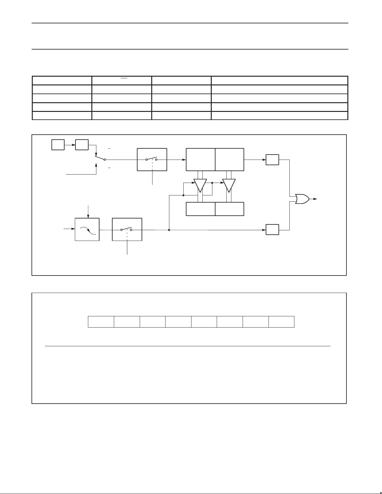
OSC
Timer n
Gate bit
INTn Pin
*d = 6 in 6-clock mode; d = 12 in 12-clock mode.
Tn Pin
÷ d*
TRn
C/T = 0
C/T = 1
Control
TLn
(5 Bits)
THn
(8 Bits)
TFn Interrupt
SU01618
Figure 2. Timer/Counter 0/1 Mode 0: 13-Bit Timer/Counter
TCON Address = 88H Reset Value = 00H
Bit Addressable
76543210
IE0IT1IE1TR0TF0TR1TF1
IT0
BIT SYMBOL FUNCTION
TCON.7 TF1 Timer 1 overflow flag. Set by hardware on Timer/Counter overflow.
Cleared by hardware when processor vectors to interrupt routine, or clearing the bit in software.
TCON.6 TR1 Timer 1 Run control bit. Set/cleared by software to turn Timer/Counter on/off.
TCON.5 TF0 Timer 0 overflow flag. Set by hardware on Timer/Counter overflow.
Cleared by hardware when processor vectors to interrupt routine, or by clearing the bit in software.
TCON.4 TR0 Timer 0 Run control bit. Set/cleared by software to turn Timer/Counter on/off.
TCON.3 IE1 Interrupt 1 Edge flag. Set by hardware when external interrupt edge detected.
Cleared when interrupt processed.
TCON.2 IT1 Interrupt 1 type control bit. Set/cleared by software to specify falling edge/low level triggered
external interrupts.
TCON.1 IE0 Interrupt 0 Edge flag. Set by hardware when external interrupt edge detected.
Cleared when interrupt processed.
TCON.0 IT0 Interrupt 0 Type control bit. Set/cleared by software to specify falling edge/low level
triggered external interrupts.
SU01516
2002 Jul 18
Figure 3. Timer/Counter 0/1 Control (TCON) Register
14
Philips Semiconductors Preliminary data
P89C51RA2/RB2/RC2/RD2xx80C51 8-bit Flash microcontroller family
8KB/16KB/32KB/64KB ISP/IAP Flash with 512B/512B/512B/1KB RAM
OSC
Timer n
Gate bit
INTn Pin
*d = 6 in 6-clock mode; d = 12 in 12-clock mode.
OSC
Timer 0
Gate bit
÷ d*
Tn Pin
TRn
÷ d*
T0 Pin
TR0
C/T = 0
C/T
= 1
Control
TLn
(8 Bits)
THn
(8 Bits)
Reload
Figure 4. Timer/Counter 0/1 Mode 2: 8-Bit Auto-Reload
C/T = 0
C/T
= 1
Control
TL0
(8 Bits)
TFn
TF0
Interrupt
SU01619
Interrupt
INT0 Pin
OSC
*d = 6 in 6-clock mode; d = 12 in 12-clock mode.
÷ d*
TH0
(8 Bits)
Control
TR1
Figure 5. Timer/Counter 0 Mode 3: Two 8-Bit Counters
TF1
Interrupt
SU01620
2002 Jul 18
15

Philips Semiconductors Preliminary data
P89C51RA2/RB2/RC2/RD2xx80C51 8-bit Flash microcontroller family
8KB/16KB/32KB/64KB ISP/IAP Flash with 512B/512B/512B/1KB RAM
TIMER 2 OPERATION
Timer 2
Timer 2 is a 16-bit Timer/Counter which can operate as either an
event timer or an event counter, as selected by C/T
function register T2CON (see Figure 6). Timer 2 has three operating
modes: Capture, Auto-reload (up or down counting), and Baud Rate
Generator, which are selected by bits in the T2CON as shown in
Table 3.
2 in the special
Capture Mode
In the capture mode there are two options which are selected by bit
EXEN2 in T2CON. If EXEN2=0, then timer 2 is a 16-bit timer or
counter (as selected by C/T
sets bit TF2, the timer 2 overflow bit. This bit can be used to
generate an interrupt (by enabling the Timer 2 interrupt bit in the
IE register). If EXEN2= 1, Timer 2 operates as described above, but
with the added feature that a 1- to -0 transition at external input
T2EX causes the current value in the Timer 2 registers, TL2 and
TH2, to be captured into registers RCAP2L and RCAP2H,
respectively. In addition, the transition at T2EX causes bit EXF2 in
T2CON to be set, and EXF2 like TF2 can generate an interrupt
(which vectors to the same location as Timer 2 overflow interrupt.
The Timer 2 interrupt service routine can interrogate TF2 and EXF2
to determine which event caused the interrupt). The capture mode is
illustrated in Figure 7 (There is no reload value for TL2 and TH2 in
this mode. Even when a capture event occurs from T2EX, the
counter keeps on counting T2EX pin transitions or osc/6 pulses
(osc/12 in 12-clock mode).).
2 in T2CON) which, upon overflowing
Auto-Reload Mode (Up or Down Counter)
In the 16-bit auto-reload mode, Timer 2 can be configured (as either
a timer or counter [C/T
or down. The counting direction is determined by bit DCEN (Down
2 in T2CON]) then programmed to count up
Counter Enable) which is located in the T2MOD register (see
Figure 8). When reset is applied the DCEN=0 which means Timer 2
will default to counting up. If DCEN bit is set, Timer 2 can count up
or down depending on the value of the T2EX pin.
Figure 9 shows Timer 2 which will count up automatically since
DCEN=0. In this mode there are two options selected by bit EXEN2
in T2CON register. If EXEN2=0, then T imer 2 counts up to 0FFFFH
and sets the TF2 (Overflow Flag) bit upon overflow. This causes the
Timer 2 registers to be reloaded with the 16-bit value in RCAP2L
and RCAP2H. The values in RCAP2L and RCAP2H are preset by
software means.
If EXEN2=1, then a 16-bit reload can be triggered either by an
overflow or by a 1-to-0 transition at input T2EX. This transition also
sets the EXF2 bit. The Timer 2 interrupt, if enabled, can be
generated when either TF2 or EXF2 are 1.
In Figure 10 DCEN=1 which enables Timer 2 to count up or down.
This mode allows pin T2EX to control the direction of count. When a
logic 1 is applied at pin T2EX Timer 2 will count up. Timer 2 will
overflow at 0FFFFH and set the TF2 flag, which can then generate
an interrupt, if the interrupt is enabled. This timer overflow also
causes the 16-bit value in RCAP2L and RCAP2H to be reloaded
into the timer registers TL2 and TH2.
When a logic 0 is applied at pin T2EX this causes Timer 2 to count
down. The timer will underflow when TL2 and TH2 become equal to
the value stored in RCAP2L and RCAP2H. Timer 2 underflow sets
the TF2 flag and causes 0FFFFH to be reloaded into the timer
registers TL2 and TH2.
The external flag EXF2 toggles when Timer 2 underflows or overflows.
This EXF2 bit can be used as a 17th bit of resolution if needed. The
EXF2 flag does not generate an interrupt in this mode of operation.
(MSB) (LSB)
TF2 EXF2 RCLK TCLK EXEN2 TR2 C/T
Symbol Position Name and Significance
TF2 T2CON.7 Timer 2 overflow flag set by a Timer 2 overflow and must be cleared by software. TF2 will not be set
EXF2 T2CON.6 Timer 2 external flag set when either a capture or reload is caused by a negative transition on T2EX and
RCLK T2CON.5 Receive clock flag. When set, causes the serial port to use Timer 2 overflow pulses for its receive clock
TCLK T2CON.4 Transmit clock flag. When set, causes the serial port to use Timer 2 overflow pulses for its transmit clock
EXEN2 T2CON.3 Timer 2 external enable flag. When set, allows a capture or reload to occur as a result of a negative
TR2 T2CON.2 Start/stop control for Timer 2. A logic 1 starts the timer.
C/T
2 T2CON.1 Timer or counter select. (Timer 2)
CP/RL
2 T2CON.0 Capture/Reload flag. When set, captures will occur on negative transitions at T2EX if EXEN2 = 1. When
when either RCLK or TCLK = 1.
EXEN2 = 1. When Timer 2 interrupt is enabled, EXF2 = 1 will cause the CPU to vector to the Timer 2
interrupt routine. EXF2 must be cleared by software. EXF2 does not cause an interrupt in up/down
counter mode (DCEN = 1).
in modes 1 and 3. RCLK = 0 causes Timer 1 overflow to be used for the receive clock.
in modes 1 and 3. TCLK = 0 causes Timer 1 overflows to be used for the transmit clock.
transition on T2EX if Timer 2 is not being used to clock the serial port. EXEN2 = 0 causes Timer 2 to
ignore events at T2EX.
0 = Internal timer (OSC/6 in 6-clock mode or OSC/12 in 12-clock mode)
1 = External event counter (falling edge triggered).
cleared, auto-reloads will occur either with Timer 2 overflows or negative transitions at T2EX when
EXEN2 = 1. When either RCLK = 1 or TCLK = 1, this bit is ignored and the timer is forced to auto-reload
on Timer 2 overflow .
Figure 6. Timer/Counter 2 (T2CON) Control Register
2 CP/RL2
SU01251
2002 Jul 18
16
Philips Semiconductors Preliminary data
P89C51RA2/RB2/RC2/RD2xx80C51 8-bit Flash microcontroller family
8KB/16KB/32KB/64KB ISP/IAP Flash with 512B/512B/512B/1KB RAM
Table 3. Timer 2 Operating Modes
RCLK + TCLK CP/RL2 TR2 MODE
0 0 1 16-bit Auto-reload
0 1 1 16-bit Capture
1 X 1 Baud rate generator
X X 0 (off)
OSC
T2 Pin
T2EX Pin
÷ n*
Transition
Detector
C/T2 = 0
C/T
2 = 1
EXEN2
Control
TR2
Control
Capture
TL2
(8 BITS)
RCAP2L RCAP2H
TH2
(8 BITS)
TF2
EXF2
* n = 6 in 6-clock mode, or 12 in 12-clock mode.
Figure 7. Timer 2 in Capture Mode
T2MOD Address = 0C9H Reset Value = XXXX XX00B
Not Bit Addressable
— — — — — — T2OE DCEN
Timer 2
Interrupt
SU01252
Bit
76543210
Symbol Function
— Not implemented, reserved for future use.*
T2OE Timer 2 Output Enable bit.
DCEN Down Count Enable bit. When set, this allows Timer 2 to be configured as an up/down counter.
* User software should not write 1s to reserved bits. These bits may be used in future 8051 family products to invoke new features.
In that case, the reset or inactive value of the new bit will be 0, and its active value will be 1. The value read from a reserved bit is
indeterminate.
Figure 8. Timer 2 Mode (T2MOD) Control Register
2002 Jul 18
17
SU00729

Philips Semiconductors Preliminary data
P89C51RA2/RB2/RC2/RD2xx80C51 8-bit Flash microcontroller family
8KB/16KB/32KB/64KB ISP/IAP Flash with 512B/512B/512B/1KB RAM
OSC
T2 PIN
T2EX PIN
÷ n*
TRANSITION
DETECTOR
C/T2 = 0
2 = 1
C/T
CONTROL
EXEN2
* n = 6 in 6-clock mode, or 12 in 12-clock mode.
Figure 9. Timer 2 in Auto-Reload Mode (DCEN = 0)
TL2
(8 BITS)
CONTROL
TR2
RELOAD
RCAP2L RCAP2H
(DOWN COUNTING RELOAD VALUE)
FFH FFH
TH2
(8 BITS)
TF2
EXF2
TOGGLE
TIMER 2
INTERRUPT
SU01253
T2 PIN
÷ n*
C/T2 = 0
C/T
2 = 1
CONTROL
TR2
OSC
* n = 6 in 6-clock mode, or 12 in 12-clock mode.
Figure 10. Timer 2 Auto Reload Mode (DCEN = 1)
TL2 TH2
OVERFLOW
RCAP2L RCAP2H
(UP COUNTING RELOAD VALUE) T2EX PIN
COUNT
DIRECTION
1 = UP
0 = DOWN
TF2
EXF2
INTERRUPT
SU01254
2002 Jul 18
18

Philips Semiconductors Preliminary data
P89C51RA2/RB2/RC2/RD2xx80C51 8-bit Flash microcontroller family
8KB/16KB/32KB/64KB ISP/IAP Flash with 512B/512B/512B/1KB RAM
Timer 1
Overflow
n = 1 in 6-clock mode
n = 2 in 12-clock mode
OSC
÷ n
T2 Pin
Transition
Detector
C/T2 = 0
2 = 1
C/T
TR2
Control
TL2
(8-bits)
RCAP2L RCAP2H
TH2
(8-bits)
Reload
÷ 2
“0” “1”
“0”“1”
“0”“1”
÷ 16
÷ 16
SMOD
RCLK
RX Clock
TCLK
TX Clock
T2EX Pin
Control
EXEN2
Note availability of additional external interrupt.
EXF2
Figure 11. T imer 2 in Baud Rate Generator Mode
Table 4. Timer 2 Generated Commonly Used
Baud Rates
Baud Rate Timer 2
12-clock
mode
6-clock
mode
Osc Freq
RCAP2H RCAP2L
375 k 750 k 12 MHz FF FF
9.6 k 19.2 k 12 MHz FF D9
4.8 k 9.6 k 12 MHz FF B2
2.4 k 4.8 k 12 MHz FF 64
1.2 k 2.4 k 12 MHz FE C8
300 600 12 MHz FB 1E
110 220 12 MHz F2 AF
300 600 6 MHz FD 8F
110 220 6 MHz F9 57
Baud Rate Generator Mode
Bits TCLK and/or RCLK in T2CON (Table 4) allow the serial port
transmit and receive baud rates to be derived from either Timer 1 or
Timer 2. When TCLK= 0, Timer 1 is used as the serial port transmit
baud rate generator . When TCLK= 1, Timer 2 is used as the serial
port transmit baud rate generator. RCLK has the same effect for the
serial port receive baud rate. With these two bits, the serial port can
have different receive and transmit baud rates – one generated by
Timer 1, the other by Timer 2.
Figure 11 shows the Timer 2 in baud rate generation mode. The baud
rate generation mode is like the auto-reload mode,in that a rollover in
TH2 causes the Timer 2 registers to be reloaded with the 16-bit value
in registers RCAP2H and RCAP2L, which are preset by software.
Timer 2
Interrupt
SU01629
The baud rates in modes 1 and 3 are determined by Timer 2’s
overflow rate given below:
Modes 1 and 3 Baud Rates +
Timer 2 Overflow Rate
16
The timer can be configured for either “timer” or “counter” operation.
In many applications, it is configured for “timer” operation (C/T
Timer operation is different for Timer 2 when it is being used as a
baud rate generator.
Usually, as a timer it would increment every machine cycle (i.e.,
1
/6 the oscillator frequency in 6-clock mode, 1/12 the oscillator
frequency in 12-clock mode). As a baud rate generator, it
increments at the oscillator frequency in 6-clock mode (
OSC
12-clock mode). Thus the baud rate formula is as follows:
Modes 1 and 3 Baud Rates =
Oscillator Frequency
[n* [65536 * (RCAP2H, RCAP2L)]]
* n = 16 in 6-clock mode
32 in 12-clock mode
Where: (RCAP2H, RCAP2L)= The content of RCAP2H and
RCAP2L taken as a 16-bit unsigned integer.
The Timer 2 as a baud rate generator mode shown in Figure 11, is
valid only if RCLK and/or TCLK = 1 in T2CON register. Note that a
rollover in TH2 does not set TF2, and will not generate an interrupt.
Thus, the Timer 2 interrupt does not have to be disabled when
Timer 2 is in the baud rate generator mode. Also if the EXEN2
(T2 external enable flag) is set, a 1-to-0 transition in T2EX
(Timer/counter 2 trigger input) will set EXF2 (T2 external flag) but
will not cause a reload from (RCAP2H, RCAP2L) to (TH2,TL2).
Therefore when Timer 2 is in use as a baud rate generator, T2EX
can be used as an additional external interrupt, if needed.
2=0).
/2 in
2002 Jul 18
19

Philips Semiconductors Preliminary data
P89C51RA2/RB2/RC2/RD2xx80C51 8-bit Flash microcontroller family
8KB/16KB/32KB/64KB ISP/IAP Flash with 512B/512B/512B/1KB RAM
When Timer 2 is in the baud rate generator mode, one should not try
to read or write TH2 and TL2. As a baud rate generator, T imer 2 is
incremented every state time (osc/2) or asynchronously from pin T2;
under these conditions, a read or write of TH2 or TL2 may not be
accurate. The RCAP2 registers may be read, but should not be
written to, because a write might overlap a reload and cause write
and/or reload errors. The timer should be turned off (clear TR2)
before accessing the Timer 2 or RCAP2 registers.
Table 4 shows commonly used baud rates and how they can be
obtained from Timer 2.
Summary of Baud Rate Equations
Timer 2 is in baud rate generating mode. If Timer 2 is being clocked
through pin T2 (P1.0) the baud rate is:
Baud Rate +
Timer 2 Overflow Rate
16
If Timer 2 is being clocked internally, the baud rate is:
f
Baud Rate +
Where f
OSC
To obtain the reload value for RCAP2H and RCAP2L, the above
equation can be rewritten as:
RCAP2H,RCAP2L + 65536 *
[n* [65536 * (RCAP2H, RCAP2L)]]
* n = 16 in 6-clock mode
= Oscillator Frequency
OSC
32 in 12-clock mode
ǒ
n* Baud Rate
Timer/Counter 2 Set-up
Except for the baud rate generator mode, the values given for T2CON
do not include the setting of the TR2 bit. Therefore, bit TR2 must be
set, separately, to turn the timer on. see Table 5 for set-up of Timer 2
as a timer. Also see Table 6 for set-up of Timer 2 as a counter.
Table 5. Timer 2 as a Timer
T2CON
MODE
16-bit Auto-Reload 00H 08H
16-bit Capture 01H 09H
Baud rate generator receive and transmit same baud rate 34H 36H
Receive only 24H 26H
Transmit only 14H 16H
INTERNAL CONTROL
(Note 1)
EXTERNAL CONTROL
f
OSC
(Note 2)
Ǔ
Table 6. Timer 2 as a Counter
TMOD
MODE
16-bit 02H 0AH
Auto-Reload 03H 0BH
NOTES:
1. Capture/reload occurs only on timer/counter overflow.
2. Capture/reload occurs on timer/counter overflow and a 1-to-0 transition on T2EX (P1.1) pin except when Timer 2 is used in the baud rate
generator mode.
INTERNAL CONTROL
(Note 1)
EXTERNAL CONTROL
(Note 2)
2002 Jul 18
20

Philips Semiconductors Preliminary data
P89C51RA2/RB2/RC2/RD2xx80C51 8-bit Flash microcontroller family
8KB/16KB/32KB/64KB ISP/IAP Flash with 512B/512B/512B/1KB RAM
FULL-DUPLEX ENHANCED UART
Standard UART operation
The serial port is full duplex, meaning it can transmit and receive
simultaneously. It is also receive-buffered, meaning it can
commence reception of a second byte before a previously received
byte has been read from the register. (However, if the first byte still
hasn’t been read by the time reception of the second byte is
complete, one of the bytes will be lost.) The serial port receive and
transmit registers are both accessed at Special Function Register
SBUF. Writing to SBUF loads the transmit register, and reading
SBUF accesses a physically separate receive register.
The serial port can operate in 4 modes:
Mode 0: Serial data enters and exits through RxD. TxD outputs
the shift clock. 8 bits are transmitted/received (LSB first).
The baud rate is fixed at 1/12 the oscillator frequency in
12-clock mode or 1/6 the oscillator frequency in 6-clock
mode.
Mode 1: 10 bits are transmitted (through TxD) or received
(through RxD): a start bit (0), 8 data bits (LSB first), and
a stop bit (1). On receive, the stop bit goes into RB8 in
Special Function Register SCON. The baud rate is
variable.
Mode 2: 1 1 bits are transmitted (through TxD) or received
(through RxD): start bit (0), 8 data bits (LSB first), a
programmable 9th data bit, and a stop bit (1). On
Transmit, the 9th data bit (TB8 in SCON) can be
assigned the value of 0 or 1. Or, for example, the parity
bit (P, in the PSW) could be moved into TB8. On receive,
the 9th data bit goes into RB8 in Special Function
Register SCON, while the stop bit is ignored. The baud
rate is programmable to either 1/32 or 1/64 the oscillator
frequency in 12-clock mode or 1/16 or 1/32 the oscillator
frequency in 6-clock mode.
Mode 3: 1 1 bits are transmitted (through TxD) or received
(through RxD): a start bit (0), 8 data bits (LSB first), a
programmable 9th data bit, and a stop bit (1). In fact,
Mode 3 is the same as Mode 2 in all respects except
baud rate. The baud rate in Mode 3 is variable.
In all four modes, transmission is initiated by any instruction that
uses SBUF as a destination register. Reception is initiated in Mode 0
by the condition RI = 0 and REN = 1. Reception is initiated in the
other modes by the incoming start bit if REN = 1.
Multiprocessor Communications
Modes 2 and 3 have a special provision for multiprocessor
communications. In these modes, 9 data bits are received. The 9th
one goes into RB8. Then comes a stop bit. The port can be
programmed such that when the stop bit is received, the serial port
interrupt will be activated only if RB8 = 1. This feature is enabled by
setting bit SM2 in SCON. A way to use this feature in multiprocessor
systems is as follows:
When the master processor wants to transmit a block of data to one
of several slaves, it first sends out an address byte which identifies
the target slave. An address byte differs from a data byte in that the
9th bit is 1 in an address byte and 0 in a data byte. With SM2 = 1, no
slave will be interrupted by a data byte. An address byte, however,
will interrupt all slaves, so that each slave can examine the received
byte and see if it is being addressed. The addressed slave will clear
its SM2 bit and prepare to receive the data bytes that will be coming.
The slaves that weren’t being addressed leave their SM2s set and
go on about their business, ignoring the coming data bytes.
SM2 has no effect in Mode 0, and in Mode 1 can be used to check
the validity of the stop bit. In a Mode 1 reception, if SM2 = 1, the
receive interrupt will not be activated unless a valid stop bit is
received.
Serial Port Control Register
The serial port control and status register is the Special Function
Register SCON, shown in Figure 12. This register contains not only
the mode selection bits, but also the 9th data bit for transmit and
receive (TB8 and RB8), and the serial port interrupt bits (TI and RI).
Baud Rates
The baud rate in Mode 0 is fixed: Mode 0 Baud Rate = Oscillator
Frequency / 12 (12-clock mode) or / 6 (6-clock mode). The baud
rate in Mode 2 depends on the value of bit SMOD in Special
Function Register PCON. If SMOD = 0 (which is the value on reset),
and the port pins in 12-clock mode, the baud rate is 1/64 the
oscillator frequency . If SMOD = 1, the baud rate is 1/32 the oscillator
frequency. In 6-clock mode, the baud rate is 1/32 or 1/16 the
oscillator frequency, respectively.
Mode 2 Baud Rate =
SMOD
2
(Oscillator Frequency)
n
Where:
n = 64 in 12-clock mode, 32 in 6-clock mode
The baud rates in Modes 1 and 3 are determined by the Timer 1 or
Timer 2 overflow rate.
Using Timer 1 to Generate Baud Rates
When Timer 1 is used as the baud rate generator (T2CON.RCLK
= 0, T2CON.TCLK = 0), the baud rates in Modes 1 and 3 are
determined by the Timer 1 overflow rate and the value of SMOD as
follows:
Mode 1, 3 Baud Rate =
SMOD
2
(Timer 1 Overflow Rate)
n
Where:
n = 32 in 12-clock mode, 16 in 6-clock mode
The Timer 1 interrupt should be disabled in this application. The
Timer itself can be configured for either “timer” or “counter”
operation, and in any of its 3 running modes. In the most typical
applications, it is configured for “timer” operation, in the auto-reload
mode (high nibble of TMOD = 0010B). In that case the baud rate is
given by the formula:
Mode 1, 3 Baud Rate =
SMOD
2
Where:
n = 32 in 12-clock mode, 16 in 6-clock mode
One can achieve very low baud rates with Timer 1 by leaving the
Timer 1 interrupt enabled, and configuring the Timer to run as a
16-bit timer (high nibble of TMOD = 0001B), and using the Timer 1
interrupt to do a 16-bit software reload. Figure 13 lists various
commonly used baud rates and how they can be obtained from
Timer 1.
Oscillator Frequency
n
12 [256–(TH1)]
2002 Jul 18
21
 Loading...