

Philips P87C750PBPN, P87C750PBDDB, P87C750EFFFA, P87C750PFPN, P87C750PFFFA Datasheet
...
83C750/87C750
80C51 8-bit microcontroller family
1K/64 OTP ROM, low pin count
Product specification
Supersedes data of 1998 Jan 19
IC20 Data Handbook
1998 May 01
INTEGRATED CIRCUITS
Philips Semiconductors Product specification
83C750/87C750
80C51 8-bit microcontroller family
1K/64 OTP/ROM, low pin count
2
1998 May 01 853–1683 19331
DESCRIPTION
The Philips 8XC750 offers the advantages of the 80C51 architecture
in a small package and at low cost.
The 8XC750 Microcontroller is fabricated with Philips high-density
CMOS technology. Philips epitaxial substrate minimizes CMOS
latch-up sensitivity.
The 87C750 contains a 1k × 8 EPROM, a 64 × 8 RAM, 19 I/O lines,
a 16-bit auto-reload counter/timer , a five-source, fixed-priority level
interrupt structure and an on-chip oscillator.
FEA TURES
•80C51 based architecture
•Oscillator frequency range—up to 16MHz
•Small package sizes
– 24-pin DIP (300 mil “skinny DIP”)
– 24-pin Shrink Small Outline Package
– 28-pin PLCC
•87C750 available in one-time programmable plastic packages
•Low power consumption:
– Normal operation: less than 11mA @ 5V, 12MHz
– Idle mode
– Power-down mode
•1k × 8 EPROM (87C750)
•64 × 8 RAM
•16-bit auto reloadable counter/timer
•Boolean processor
•CMOS and TTL compatible
•Well suited for logic replacement, consumer and industrial
applications
•LED drive outputs
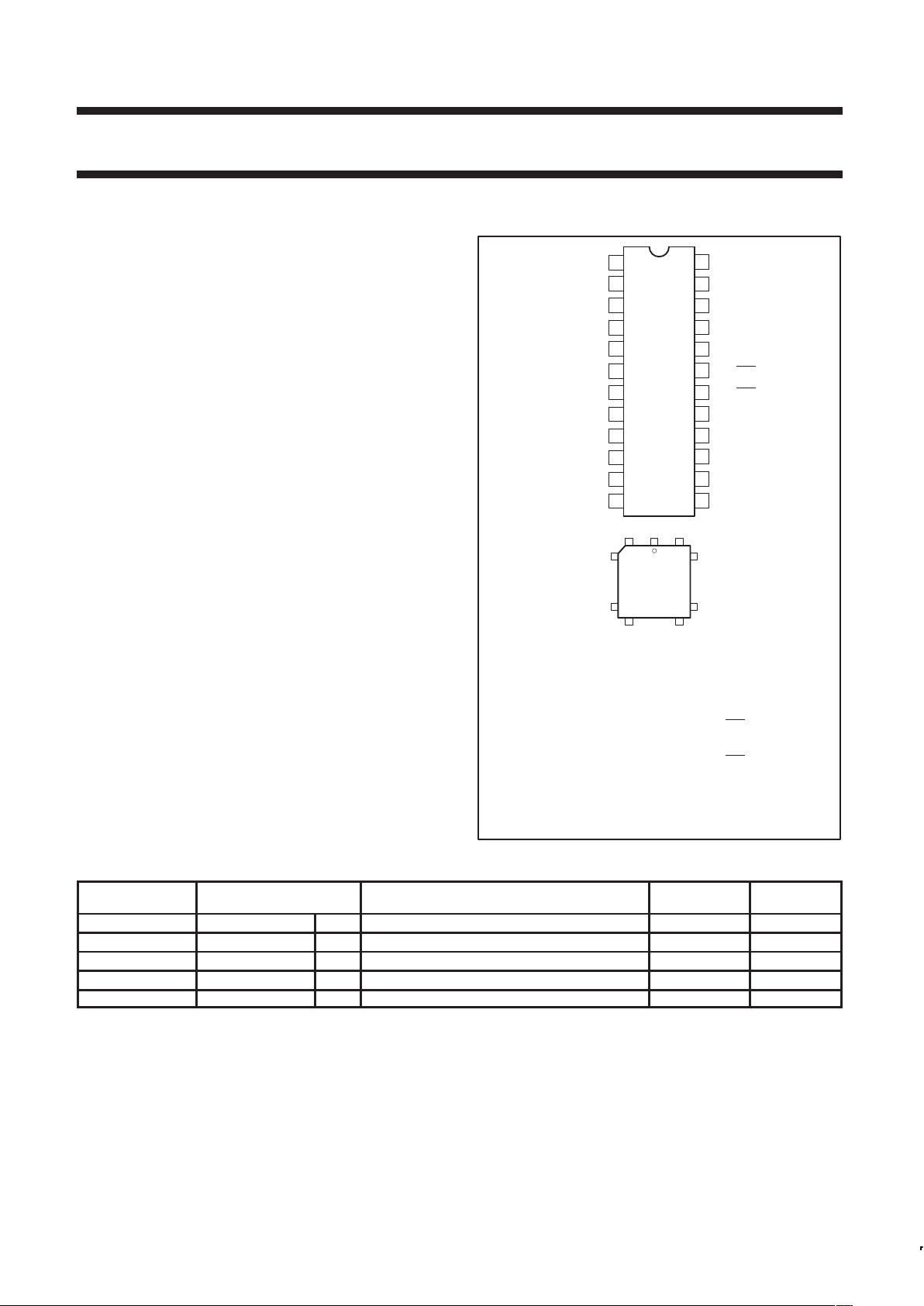
PIN CONFIGURATIONS
1
2
3
4
5
6
7
8
9
10
11
12
13
14
15
16
17
18
19
20
21
22
23
24
P3.4/A4
P3.3/A3
P3.2/A2/A10
P3.1/A1/A9
P3.0/A0/A8
P0.2/V
PP
RST
X2
X1
V
SS
P0.0/ASEL
P1.0/D0
P1.1/D1
P1.2/D2
P1.3/D3
P1.4/D4
P1.5/INT0/D5
P1.6/INT1/D6
P1.7/T0/D7
P3.7/A7
P3.6/A6
P3.5/A5
V
CC
PLASTIC
DUAL
IN-LINE
AND
SHRINK
SMALL
OUTLINE
PACKAGE
PLASTIC
LEADED
CHIP
CARRIER
4126
5
11
25
19
12 18
P0.1/OE–PGM
Pin Function
1 P3.4/A4
2 P3.3/A3
3 P3.2/A2/A10
4 P3.1/A1/A9
5 NC*
6 P3.0/A0/A8
7 P0.2/V
PP
8 P0.1/OE-PGM
9 P0.0/ASEL
10 NC*
11 RST
12 X2
13 X1
14 V
SS
Pin Function
15 P1.0/D0
16 P1.1/D1
17 P1.2/D2
18 P1.3/D3
19 P1.4/D4
20 P1.5/INT0
/D5
21 NC*
22 NC*
23 P1.6/INT1/D6
24 P1.7/T0/D7
25 P3.7/A7
26 P3.6/A6
27 P3.5/A5
28 V
CC
SU00295A
* NO INTERNAL CONNECTION
ORDERING INFORMATION
ROM EPROM
1
TEMPERATURE RANGE °C AND PACKAGE FREQUENCY
DRAWING
NUMBER
P83C750EBP N P87C750EBP N OTP 0 to +70, Plastic Dual In-line Package 3.5 to 16MHz SOT222-1
P83C750EFP N P87C750EFP N OTP –40 to +85, Plastic Dual In-line Package 3.5 to 16MHz SOT222-1
P83C750EBA A P87C750EBA A OTP 0 to +70, Plastic Lead Chip Carrier 3.5 to 16MHz SOT261-3
P83C750EFA A P87C750EFA A OTP –40 to +85, Plastic Lead Chip Carrier 3.5 to 16MHz SOT261-3
P83C750EBD DB P87C750EBD DB OTP 0 to +70, Shrink Small Outline Package 3.5 to 16MHz SOT340-1
NOTE:
1. OTP = One Time Programmable EPROM.
Philips Semiconductors Product specification
83C750/87C750
80C51 8-bit microcontroller family
1K/64 OTP/ROM, low pin count
1998 May 01
3
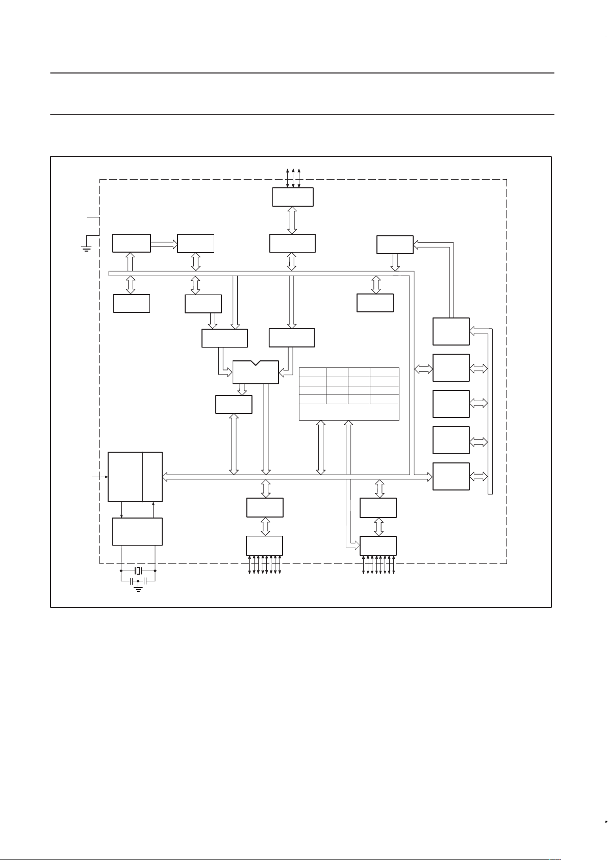
BLOCK DIAGRAM
RST
X1
X2
V
CC
V
SS
RAM
EPROM
ACC
TMP2
TMP1
ALU
INSTRUCTION
REGISTER
PD
OSCILLATOR
PSW
BUFFER
DPTR
PCON TCON
IE
TH0 TL0
RTH RTL
INTERRUPT AND
TIMER BLOCKS
P1.0–P1.7
P3.0–P3.7
P0.0–P0.2
PORT 0
DRIVERS
RAM ADDR
REGISTER
PORT 0
LATCH
STACK
POINTER
PROGRAM
ADDRESS
REGISTER
PC
INCRE-
MENTER
PROGRAM
COUNTER
PORT 3
DRIVERS
PORT 1
DRIVERS
PORT 3
LATCH
PORT 1
LATCH
TIMING
AND
CONTROL
B
REGISTER
SU00312
Philips Semiconductors Product specification
83C750/87C750
80C51 8-bit microcontroller family
1K/64 OTP/ROM, low pin count
1998 May 01
4
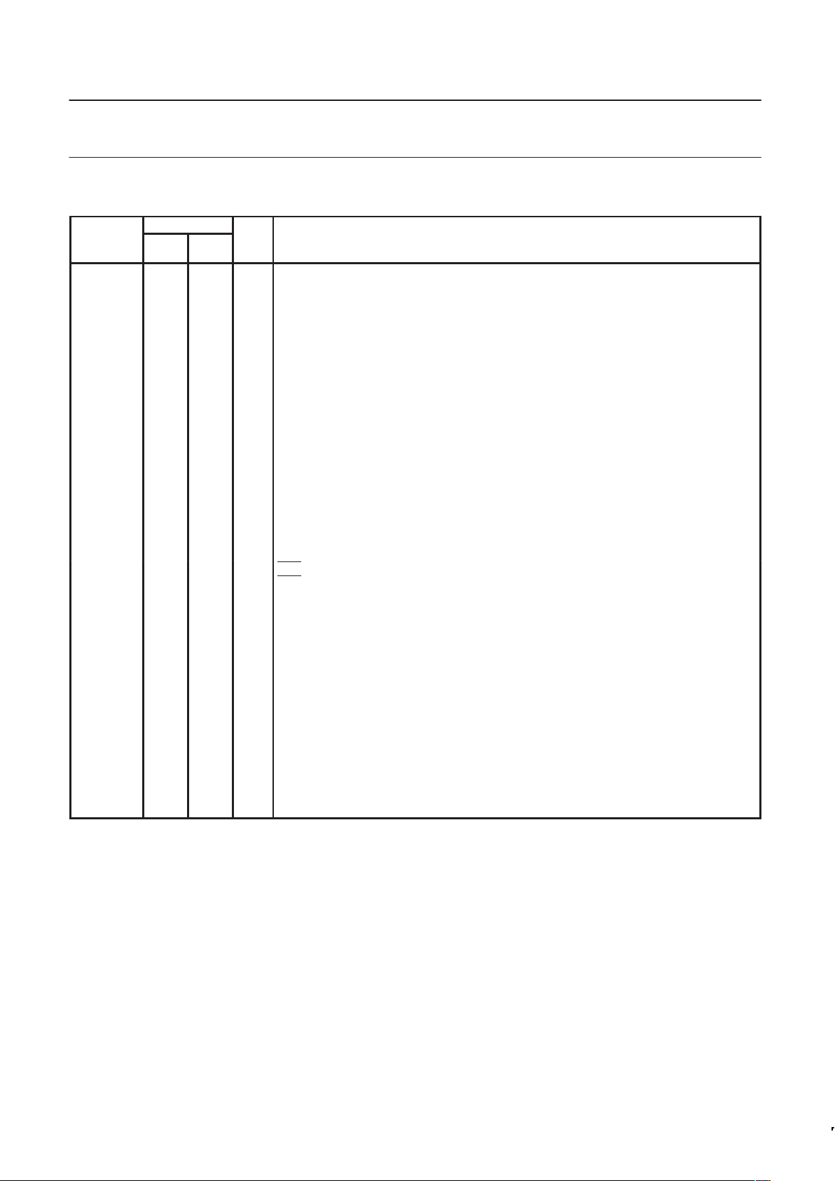
PIN DESCRIPTIONS
PIN NO.
MNEMONIC DIP/
SSOP
LCC TYPE NAME AND FUNCTION
V
SS
12 14 I Circuit Ground Potential
V
CC
24 28 I Supply voltage during normal, idle, and power-down operation.
P0.0-P0.2 8-6 9-7 I/O Port 0: Port 0 is a 3-bit open-drain, bidirectional port. Port 0 pins that have 1s written to them float,
and in that state can be used as high-impedance inputs. These pins are driven low if the port register
bit is written with a 0. The state of the pin can always be read from the port register by the program.
P0.0, P0.1, and P0.2 are open drain bidirectional I/O pins with the electrical characteristics listed in
the tables that follow. While these differ from “standard TTL” characteristics, they are close enough
for the pins to still be used as general-purpose I/O. Port 0 also provides alternate functions for
programming the EPROM memory as follows:
6 7 N/A VPP (P0.2) – Programming voltage input. (See Note 1.)
7 8 I OE/PGM (P0.1) – Input which specifies verify mode (output enable) or the program mode.
OE/PGM = 1 output enabled (verify mode).
OE/PGM = 0 program mode.
8 9 I ASEL (P0.0) – Input which indicates which bits of the EPROM address are applied to port 3.
ASEL = 0 low address byte available on port 3.
ASEL = 1 high address byte available on port 3 (only the three least significant bits are used).
P1.0-P1.7 13-20 15-20,
23, 24
I/O Port 1: Port 1 is an 8-bit bidirectional I/O port with internal pull-ups. Port 1 pins that have 1s written
to them are pulled high by the internal pull-ups and can be used as inputs. As inputs, port 1 pins
that are externally pulled low will source current because of the internal pull-ups. (See DC
Electrical Characteristics: I
IL
). Port 1 serves to output the addressed EPROM contents in the verify
mode and accepts as inputs the value to program into the selected address during the program
mode. Port 1 also serves the special function features of the 80C51 family as listed below:
18 20 I INT0 (P1.5): External interrupt.
19 23 I INT1 (P1.6): External interrupt.
20 24 I T0 (P1.7): Timer 0 external input.
P3.0-P3.7 5-1,
23-21
6, 4-1,
27-25
I/O Port 3: Port 3 is an 8-bit bidirectional I/O port with internal pull-ups. Port 3 pins that have 1s written
to them are pulled high by the internal pull-ups and can be used as inputs. As inputs, port 3 pins
that are externally being pulled low will source current because of the pull-ups. (See DC Electrical
Characteristics: I
IL
). Port 3 also functions as the address input for the EPROM memory location to
be programmed (or verified). The 10-bit address is multiplexed into this port as specified by
P0.0/ASEL.
RST 9 11 I Reset: A high on this pin for two machine cycles while the oscillator is running, resets the device.
An internal diffused resistor to V
SS
permits a power-on RESET using only an external capacitor to
V
CC
. After the device is reset, a 10-bit serial sequence, sent LSB first, applied to RESET, places
the device in the programming state allowing programming address, data and V
PP
to be applied for
programming or verification purposes. The RESET serial sequence must be synchronized with the
X1 input.
X1 11 13 I Crystal 1: Input to the inverting oscillator amplifier and input to the internal clock generator circuits.
X1 also serves as the clock to strobe in a serial bit stream into RESET to place the device in the
programming state.
X2 10 12 O Crystal 2: Output from the inverting oscillator amplifier.
NOTE:
1. When P0.2 is at or close to 0 Volt, it may affect the internal ROM operation. We recommend that P0.2 be tied to V
CC
via a small pull-up (e.g.,
2kΩ).
OSCILLA T OR CHARACTERISTICS
X1 and X2 are the input and output, respectively, of an inverting
amplifier which can be configured for use as an on-chip oscillator.
To drive the device from an external clock source, X1 should be
driven while X2 is left unconnected. There are no requirements on
the duty cycle of the external clock signal, because the input to the
internal clock circuitry is through a divide-by-two flip-flop. However,
minimum and maximum high and low times specified in the data
sheet must be observed.
RESET
A reset is accomplished by holding the RST pin high for at least two
machine cycles (24 oscillator periods), while the oscillator is running.
To insure a good power-up reset, the RST pin must be high long
enough to allow the oscillator time to start up (normally a few
milliseconds) plus two machine cycles. At power-up, the voltage on
V
CC
and RST must come up at the same time for a proper start-up.
IDLE MODE
In idle mode, the CPU puts itself to sleep while all of the on-chip
peripherals stay active. The instruction to invoke the idle mode is the
last instruction executed in the normal operating mode before the
idle mode is activated. The CPU contents, the on-chip RAM, and all
of the special function registers remain intact during this mode. The
idle mode can be terminated either by any enabled interrupt (at
which time the process is picked up at the interrupt service routine
and continued), or by a hardware reset which starts the processor in
the same manner as a power-on reset.
Philips Semiconductors Product specification
83C750/87C750
80C51 8-bit microcontroller family
1K/64 OTP/ROM, low pin count
1998 May 01
5
POWER-DOWN MODE
In the power-down mode, the oscillator is stopped and the
instruction to invoke power-down is the last instruction executed.
Only the contents of the on-chip RAM are preserved. A hardware
reset is the only way to terminate the power-down mode. the control
bits for the reduced power modes are in the special function register
PCON.
Table 1. External Pin Status During Idle and
Power-Down Modes
MODE Port 0 Port 1 Port 2
Idle Data Data Data
Power-down Data Data Data
DIFFERENCES BETWEEN THE 8XC750 AND THE
80C51
Program Memory
On the 8XC750, program memory is 1024 bytes long and is not
externally expandable, so the 80C51 instructions MOVX, LJMP, and
LCALL are not implemented. The only fixed locations in program
memory are the addresses at which execution is taken up in
response to reset and interrupts, which are as follows:
Program Memory
Event Address
Reset 000
External INT0
003
Counter/timer 0 00B
External INT1
013
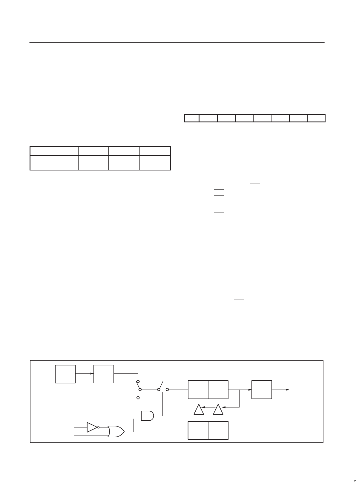
Counter/Timer Subsystem
Timer/Counter
The 8XC750 has one timers: a 16-bit timer/counter. The 16-bit
timer/counter’s operation is similar to mode 2 operation on the
80C51, but is extended to 16 bits. The timer/counter is clocked by
either 1/12 the oscillator frequency or by transitions on the T0 pin.
The C/T pin in special function register TCON selects between
these two modes. When the TCON TR bit is set, the timer/counter is
enabled. Register pair TH and TL are incremented by the clock
source. When the register pair overflows, the register pair is
reloaded with the values in registers RTH and RTL. The value in the
reload registers is left unchanged. See the 83C750 counter/timer
block diagram in Figure 1. The TF bit in special function register
TCON is set on counter overflow and, if the interrupt is enabled, will
generate an interrupt.
TCON Register
MSB LSB
GATE
C/T TF TR IE0 IT0 IE1 IT1
GATE 1 – Timer/counter is enabled only when INT0 pin is high,
and TR is 1.
0 – Timer/counter is enabled when TR is 1.
C/T 1 – Counter/timer operation from T0 pin.
0 – Timer operation from internal clock.
TF 1 – Set on overflow of TH.
0 – Cleared when processor vectors to interrupt routine
and by reset.
TR 1 – Timer/counter enabled.
0 – Timer/counter disabled.
IE0 1 – Edge detected in INT0
.
IT0 1 – INT0
is edge triggered.
0 – INT0
is level sensitive.
IE1 1 – Edge detected on INT1
.
IT1 1 – INT1
is edge triggered.
0 – INT1
is level sensitive.
These flags are functionally identical to the corresponding 80C51
flags, except that there is only one timer on the 83C750 and the
flags are therefore combined into one register.
Note that the positions of the IE0/IT0 and IE1/IT1 bits are
transposed from the positions used in the standard 80C51 TCON
register.
Interrupt Subsystem – Fixed Priority
The IP register and the 2-level interrupt system of the 80C51 are
eliminated. Simultaneous interrupt conditions are resolved by a
single-level, fixed priority as follows:
Highest priority: Pin INT0
Counter/timer flag 0
Pin INT1
Special Function Register Addresses
Special function registers for the 8XC750 are identical to those of
the 80C51, except for the changes listed below:
80C51 special function registers not present in the 8XC750 are
TMOD (89), P2 (A0) and IP (B8). The 80C51 registers TH1 and TL1
are replaced with the 87C750 registers RTH and RTL respectively
(refer to Table 2).
OSC
÷ 12
TL TH TF
RTL RTH
T0 Pin
TR
Gate
INT0
Pin
Int.
C/T = 0
C/T = 1
Reload
SU00300
Figure 1. 83C751 Counter/Timer Block Diagram
 Loading...