Philips NE5539 Service Manual

RF COMMUNICATIONS PRODUCTS
NE/SE5539
High frequency operational amplifier
Product specification April 15, 1992
IC11
Philips Semiconductors

Philips Semiconductors Product specification
NE/SE5539High frequency operational amplifier
DESCRIPTION
The NE/SE5539 is a very wide bandwidth, high slew rate, monolithic
operational amplifier for use in video amplifiers, RF amplifiers, and
extremely high slew rate amplifiers.
Emitter-follower inputs provide a true differential input impedance
device. Proper external compensation will allow design operation
over a wide range of closed-loop gains, both inverting and
non-inverting, to meet specific design requirements.
FEA TURES
•Bandwidth
– Unity gain - 350MHz
– Full power - 48MHz
– GBW - 1.2GHz at 17dB
•Slew rate: 600/Vµs
•A
: 52dB typical
VOL
•Low noise - 4nV√Hz typical
•MIL-STD processing available
APPLICA TIONS
•High speed datacom
•Video monitors & TV
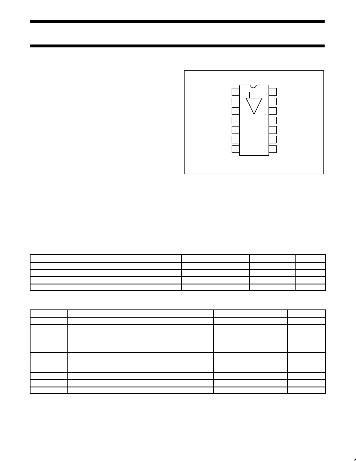
PIN CONFIGURA TION
D, F, N Packages
OS
A
V
NC
NC
ADJ
ADJ
NC
1
2
3
4
5
/
6
7
+ INPUT
-V
SUPPLY
V
GROUND
Top View
Figure 1. Pin Configuration
•Satellite communications
•Image processing
•RF instrumentation & oscillators
•Magnetic storage
•Military communications
+–
14
- INPUT
13
NC
FREQUENCY
12
COMPENS.
NC
11
10
+V
9
NC
8
OUTPUT
SL00570
ORDERING INFORMATION
DESCRIPTION TEMPERATURE RANGE ORDER CODE DWG #
14-Pin Plastic Dual In-Line Package (DIP) 0 to +70°C NE5539N SOT27-1
14-Pin Plastic Small Outline (SO) package 0 to +70°C NE5539D SOT108-1
14-Pin Ceramic Dual In-Line Package 0 to +70°C NE5539F 0581B
14-Pin Ceramic Dual In-Line Package -55 to +125°C SE5539F 0581B
ABSOLUTE MAXIMUM RATINGS
SYMBOL
V
CC
P
DMAX
T
A
T
STG
T
J
T
SOLD
NOTES:
1. Differential input voltage should not exceed 0.25V to prevent excesive input bias current and common-mode voltage 2.5V. These voltage
limits may be exceeded if current is limited to less than 10mA.
2. Derate above 25°C, at the following rates:
Supply voltage ±12 V
Maximum power dissipation,
= 25°C (still-air)
T
A
F package
N package
D package
Operating temperature range
NE
SE
Storage temperature range -65 to +150 °C
Max junction temperature 150 °C
Lead soldering temperature (10sec max) +300 °C
F package at 9.3mW/°C
N package at 11.6mW/°C
D package at 7.9mW/°C
1
PARAMETER RATING UNITS
2
1.17
1.45
0.99
0 to 70
-55 to +125
W
W
W
°C
°C
1992 Apr 15 853-0814 06456
2

Philips Semiconductors Product specification
SYMBOL
PARAMETER
TEST CONDITIONS
UNITS
CMRR
C
dB
NE/SE5539High frequency operational amplifier
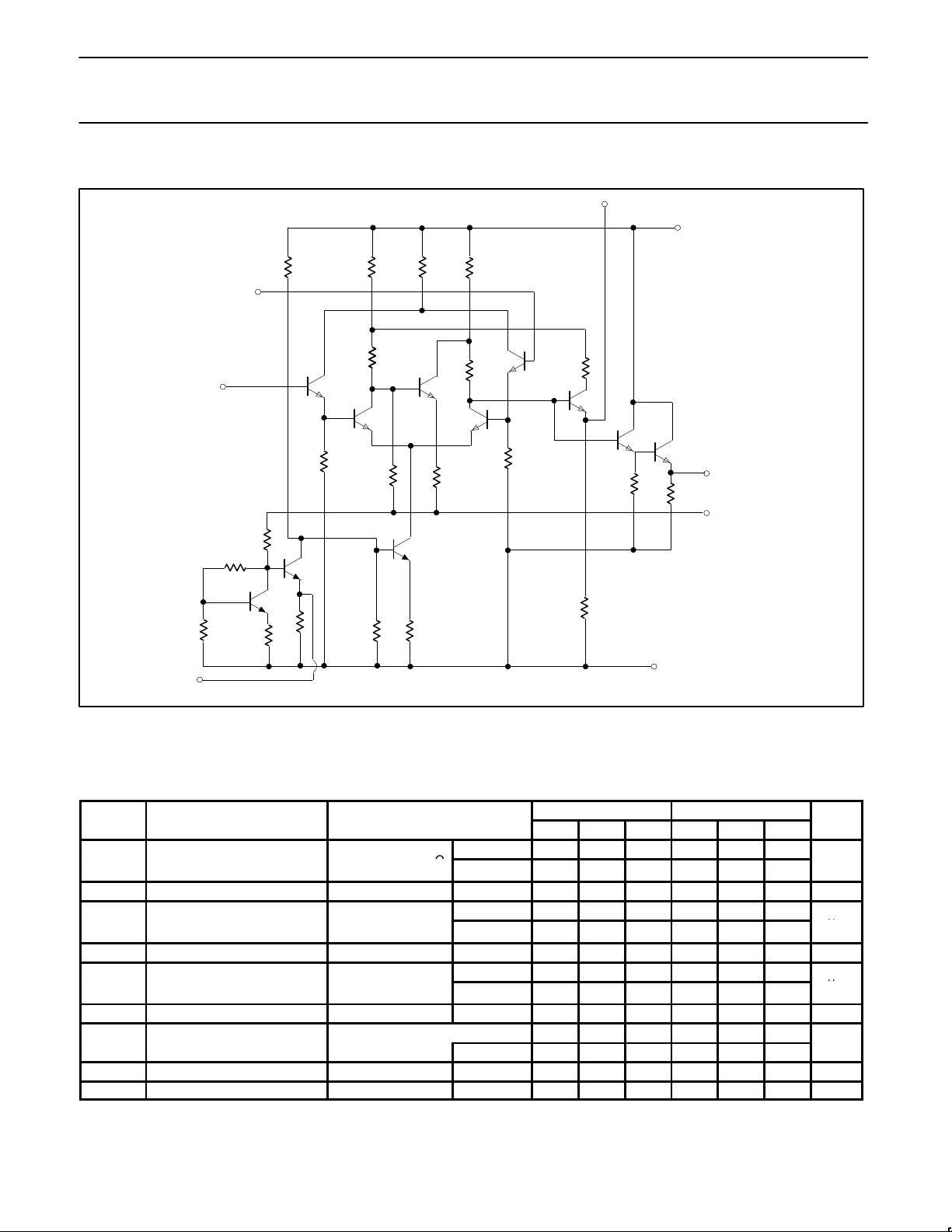
EQUIVALENT CIRCUIT
(12) FREQUENCY COMP.
(10) +V
CC
(–) 14
INVERTING INPUT
(+) 1
NON–INVERTING
INPUT
5
R
18
Q
R
R
13
Q
R
11
R
12
R
14
10
Q
11
R
15
R
R
1
Q
2
20
R
1
R
16
R
19
2
Q
9
R
17
R
3
Q
5
Q
6
R
6
4
Q
3
R
4
R
8
Q
5
Q
7
Q
R
21
R
7
8
R
2.2k
(8) OUTPUT
10
(7) GRD
CC
SL00571
R
9
(3) –V
Figure 2. Equivalent Circuit
DC ELECTRICAL CHARACTERISTICS
VCC = ±8V, TA = 25°C; unless otherwise specified.
V
I
R
R
1992 Apr 15
Input offset voltage VO = 0V, RS = 100Ω
OS
∆VOS/∆T 5 5 µV/°C
Input offset current
OS
∆IOS/∆T 0.5 0.5 nA/°C
I
Input bias current
B
∆IB/∆T 10 10 nA/°C
ommon mode rejection ratio
Input impedance 100 100 kΩ
IN
Output impedance 10 10 Ω
OUT
F = 1kHz, RS = 100Ω, VCM ±1.7V 70 80 70 80
SE5539 NE5539
MIN TYP MAX MIN TYP MAX
Over temp 2 5
TA = 25°C
2 3 2.5 5
Over temp 0.1 3
TA = 25°C
0.1 1 2
Over temp 6 25
TA = 25°C
5 13 5 20
Over temp 70 80
3
mV
µA
µA

Philips Semiconductors Product specification
SYMBOL
PARAMETER
TEST CONDITIONS
UNITS
V
Output
V
I
Positi
t
A
I
N
t
A
PSRR
P
V/V
A
VOL
Large signal voltage gain
dB
A
VOL
Large signal voltage gain
dB
SYMBOL
PARAMETER
TEST CONDITIONS
UNITS
VOSI
V
IOSI
t
A
IBI
t
A
I
Positi
t
A
I
N
t
A
PSRR
P
∆V
±1V
V/V
V
Output
V
NE/SE5539High frequency operational amplifier
DC ELECTRICAL CHARACTERISTICS (Continued)
VCC = ±8V, TA = 25°C; unless otherwise specified.
SE5539 NE5539
MIN TYP MAX MIN TYP MAX
V
A
A
A
OUT
OUT
CC+
CC-
VOL
VOL
VOL
Output voltage swing
voltage swing
ve supply curren
egative supply curren
ower supply rejection ratio
Large signal voltage gain
Large signal voltage gain
Large signal voltage gain
RL = 150Ω to GND and
470Ω to -V
CC
RL = 25Ω to GND
Over temp
RL = 25Ω to GND
= 25°C
T
A
VO = 0, R1 = ∞, Over temp 14 18
VO = 0, R1 = ∞, TA = 25°C 14 17 14 18
VO = 0, R1 = ∞, Over temp 11 15
VO = 0, R1 = ∞, TA = 25°C 11 14 11 15
∆VCC = ±1V, Over temp 300 1000
∆VCC = ±1V, TA = 25°C 200 1000
VO = +2.3V , -1.7V, RL = 150Ω to
GND, 470Ω to -V
VO = +2.3V , -1.7V
RL = 2Ω to GND TA = 25°C 47 52 57
VO = +2.5V , -2.0V
RL = 2Ω to GND TA = 25°C 48 53 58
+Swing
-Swing
+Swing
-Swing
+Swing
-Swing
CC
Over
temp
Over
temp
+2.3
+3.0
-1.5
+2.5
-2.0
-2.1
+3.1
-2.7
46 60
+2.3
+2.7
-1.7
-2.2
47 52 57 dB
V
m
m
µ
dB
dB
DC ELECTRICAL CHARACTERISTICS
VCC = ±6V, TA = 25°C; unless otherwise specified.
SE5539
MIN TYP MAX
nput offset voltage
nput offset curren
nput bias curren
CMRR Common-mode rejection ratio VCM = ±1.3V, RS = 100Ω 70 85 dB
CC+
CC-
ve supply curren
egative supply curren
ower supply rejection ratio
CC
=
Over +Swing +1.4 +2.0
OUT
voltage swing
RL = 150Ω to GND temp –Swing –1.1 –1.7
and 390Ω to –V
CC
TA = +Swing +1.5 +2.0
25°C –Swing –1.4 –1.8
Over temp 2 5
TA = 25°C 2 3
Over temp 0.1 3
TA = 25°C 0.1 1
Over temp 5 20
TA = 25°C 4 10
Over temp 11 14
TA = 25°C 11 13
Over temp 8 11
TA = 25°CmA 8 10
Over temp 300 1000
TA = 25°C
m
µ
µ
m
m
µ
1992 Apr 15
4
 Loading...