

Philips NE5534AN, NE5534D, NE5534N, NE5534AD, NE5533N Datasheet
...
Philips Semiconductors Linear Products Product specification
NE5533/5533A/
NE/SA/SE5534/5534A
Dual and single low noise op amp
114
August 31, 1994 853-0222 13721
DESCRIPTION
The 5533/5534 are dual and single high-performance low noise
operational amplifiers. Compared to other operational amplifiers,
such as TL083, they show better noise performance, improved
output drive capability and considerably higher small-signal and
power bandwidths.
This makes the devices especially suitable for application in high
quality and professional audio equipment, in instrumentation and
control circuits and telephone channel amplifiers. The op amps are
internally compensated for gain equal to, or higher than, three. The
frequency response can be optimized with an external
compensation capacitor for various applications (unity gain amplifier,
capacitive load, slew rate, low overshoot, etc.) If very low noise is of
prime importance, it is recommended that the 5533A/5534A version
be used which has guaranteed noise specifications.
FEATURES
•Small-signal bandwidth: 10MHz
•Output drive capability: 600Ω, 10V
RMS
at VS=±18V
•Input noise voltage:
4
nVH
z
•DC voltage gain: 100000
•AC voltage gain: 6000 at 10kHz
•Power bandwidth: 200kHz
•Slew rate: 13V/µs
•Large supply voltage range: ±3 to ±20V
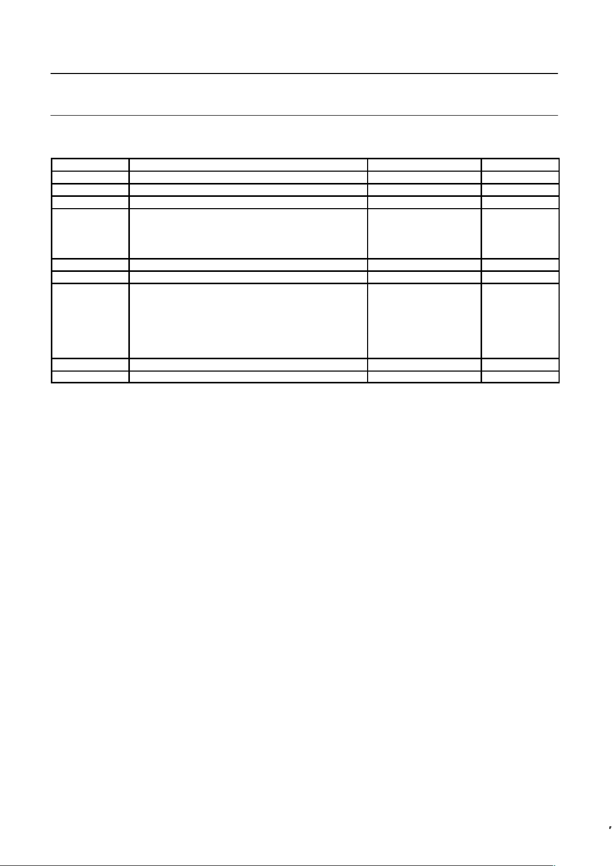
PIN CONFIGURATIONS
8
7
6
54
3
2
1
BALANCE/ COMPENSATION
V+
OUTPUT
COMPENSATION
BALANCE
INVERTING INPUT
NON-INVERTING
V-
NE/SA/SE5534/5534A
D, FE, N Packages
1
2
3
4
5
6
7
8
9
10
11
12
14
13
NE5533/5533A
N Package
INV INPUT A
NON–INV INPUT A
BALANCE A
V–
BALANCE B
NON–INV B
INV B
BAL COMP A
COMP A
OUTPUT A
V+
OUTPUT B
COMP B
BAL COMP B
TOP VIEW
TOP VIEW
APPLICATIONS
•Audio equipment
•Instrumentation and control circuits
•Telephone channel amplifiers
•Medical equipment
ORDERING INFORMATION
DESCRIPTION TEMPERATURE RANGE ORDER CODE DWG #
14-Pin Plastic Dual In-Line Package (DIP) 0 to +70°C NE5533N 0405B
14-Pin Plastic Dual In-Line Package (DIP) 0 to +70°C NE5533AN 0405B
8-Pin Plastic Small Outline (SO) package 0 to +70°C NE5534D 0174C
8-Pin Hermetic Ceramic Dual In-Line Package (CERDIP) 0 to +70°C NE5534FE
8-Pin Plastic Dual In-Line Package (DIP) 0 to +70°C NE5534N 0404B
8-Pin Plastic Small Outline (SO) package 0 to +70°C NE5534AD 0174C
8-Pin Hermetic Ceramic Dual In-Line Package (CERDIP) 0 to +70°C NE5534AF
8-Pin Plastic Dual In-Line Package (DIP) 0 to +70°C NE5534AN 0404B
8-Pin Plastic Dual In-Line Package (DIP) -40°C to +85°C SA5534N 0404B
8-Pin Plastic Small Outline (SO) package -40°C to +85°C SA5534AD 0174C
8-Pin Plastic Dual In-Line Package (DIP) -55°C to +125°C SE5534N 0404B
8-Pin Hermetic Ceramic Dual In-Line Package (CERDIP) -55°C to +125°C SE5534AF
8-Pin Plastic Dual In-Line Package (DIP) -55°C to +125°C SE5534AN 0404B
8-Pin Plastic Dual In-Line Package (DIP) -40°C to +85°C SA5534AN 0404B
Philips Semiconductors Linear Products Product specification
NE5533/5533A/
NE/SA/SE5534/5534A
Dual and single low noise op amp
August 31, 1994
115
ABSOLUTE MAXIMUM RATINGS
SYMBOL PARAMETER RATING UNIT
V
S
Supply voltage ±22 V
V
IN
Input voltage ±V supply V
V
DIFF
Differential input voltage
1
±0.5 V
T
A
Operating temperature range
SE -55 to +125 °C
SA -40 to +85 °C
NE 0 to +70 °C
T
STG
Storage temperature range -65 to +150 °C
T
J
Junction temperature 150 °C
P
D
Power dissipation at 25°C
2
16D Pkg 1350 mW
16N Pkg 1500 mW
8D Pkg 750 mW
8FE Pkg 800 mW
8N Pkg 1150 mW
Output short-circuit duration
3
Indefinite
T
SOLD
Lead soldering temperature (10sec max) 300 °C
NOTES:
1. Diodes protect the inputs against over voltage. Therefore, unless current-limiting resistors are used, large currents will flow if the differential
input voltage exceeds 0.6V. Maximum current should be limited to ±10mA.
2. For operation at elevated temperature, derate packages based on the following junction-to-ambient thermal resistance:
8-pin ceramic DIP 150°C/W
8-pin plastic DIP 105°C/W
8-pin plastic SO 160°C/W
16-pin plastic DIP 80°C/W
16-pin plastic SO 90°C/W
3. Output may be shorted to ground at V
S
=±15V, TA=25°C. Temperature and/or supply voltages must be limited to ensure dissipation rating is
not exceeded.
Philips Semiconductors Linear Products Product specification
NE5533/5533A/
NE/SA/SE5534/5534A
Dual and single low noise op amp
August 31, 1994
116
DC ELECTRICAL CHARACTERISTICS
TA=25°C, VS=±15V, unless otherwise specified.
1, 2, 3
SYMBOL
PARAMETER
TEST CONDITIONS
SE5534/5534A
NE5533/5533A
NE/SA5534/5534A
UNIT
SYMBOL
PARAMETER
TEST CONDITIONS
Min Typ Max Min Typ Max
UNIT
V
OS
0.5 2 0.5 4 mV
Offset voltage Over temperature 3 5 mV
∆VOS/∆T 5 5 µV/°C
I
OS
10 200 20 300 nA
Offset current Over temperature 500 400 nA
∆IOS/∆T 200 200 pA/°C
I
B
400 800 500 1500 nA
Input current Over temperature 1500 2000 nA
∆IB/∆T 5 5 nA/°C
I
CC
Supply current
per op amp
Over temperature
4 6.5
9
4 8
10
mA
mA
V
CM
Common mode input range ±12 ±13 ±12 ±13 V
CMRR Common mode rejection ratio 80 100 70 100 dB
PSRR Power supply rejection ratio 10 50 10 100 µV/V
A
VOL
Large-signal voltage gain
RL≥600Ω, VO=±10V
Over temperature
5025100 2515100 V/mV
V/mV
V
OUT
Output swing
RL≥600Ω
Over temperature
R
L
≥600Ω, VS=±18V
R
L
≥2kΩ
Over temperature
±12
±10
±15
±13
±12
±13
±12
±16
±13.5
±12.5
±12
±10
±15
±13
±12
±13
±12
±16
±13.5
±12.5
V
V
V
V
V
R
IN
Input resistance 50 100 30 100 kΩ
I
SC
Output short circuit current 38 38 mA
NOTES:
1. For NE5533/5533A/5534/5534A, T
MIN
= 0°C, T
MAX
= 70°C
2. For SE5534/5534A, T
MIN
= -55°C, T
MAX
= +125°C
3. For SA5534/5534A, T
MIN
= -40°C, T
MAX
= +125°C
 Loading...