Philips NE529D, NE529NB, NE529N Datasheet

0 (0)
Philips NE529D, NE529NB, NE529N Datasheet

Philips Semiconductors Linear Products

Product specification


Voltage comparator

NE529


DESCRIPTION

The NE529 is a high-speed analog voltage comparator which, for the first time, mates state-of-the-art Schottky diode technology with the conventional linear process. This allows simultaneous fabrication of high-speed TTL gates with a precision linear amplifier on a single monolithic chip.

FEATURES

10ns propagation delay

Complementary output gates

TTL or ECL compatible outputs

Wide common-mode and differential voltage range

Typical gain 5000

PIN CONFIGURATIONS

D, N Packages

V1 +

1


14

V2 +


NC


STROBE A

2


13

INPUT A

3


12

NC

INPUT B

4


11

OUTPUT A

NC

5


10

GND


V1 ±


6


9

OUTPUT B


NC

7


8

STROBE B


TOP VIEW

APPLICATIONS

BLOCK DIAGRAM


A/D conversion


V1 +


STROBE A


V2 +


ECL-to-TTL interface

INPUT A


OUTPUT A


TTL-to-ECL interface


Memory sensing

INPUT B


OUTPUT B


Optical data coupling


ORDERING INFORMATION


V1 ±

STROBE B


DESCRIPTION


TEMPERATURE RANGE


ORDER CODE


DWG #


14-Pin Plastic Dual In-Line Package (DIP)


0 to +70°C


NE529N


0405B


14-Pin Small Outline (SO) Package


0 to +70°C


NE529D


0175D


V1 +


STROBE A


V2 +

R1

20K


1K

1K


R15

4K

R16

1.5K

R17

55


R13

R14


Q3


D1


Q17


D2

R2

R3


D10


Q18


R18

4K

OUTPUT A

D3

1.5K

1.5K


750

750


R10


Q26


R11

R12


20K


Q15


Q4

Q5

Q12

Q13

Q14


Q19


R21

R22


55

250

R20


D4


D5


6.13K

4K

1.5K


R23

R19

500


R9


INPUT A


INPUT B


Q10 Q11


Q23


Q20

GND


Q1

Q2


Q24


D6


R24


OUTPUT B


4K


Q6

Q7

Q8

Q9

D7

Q21

Q22


Q27


D8


Q25


250

R25


R5


R4

200

R6

R7

R8


R26

500


V1 ±

300

300

100

200

D9


D11


Q26


STROBE B


August 31, 1994


320


853-0902 13721

Philips Semiconductors Linear Products

Product specification


Voltage comparator

NE529


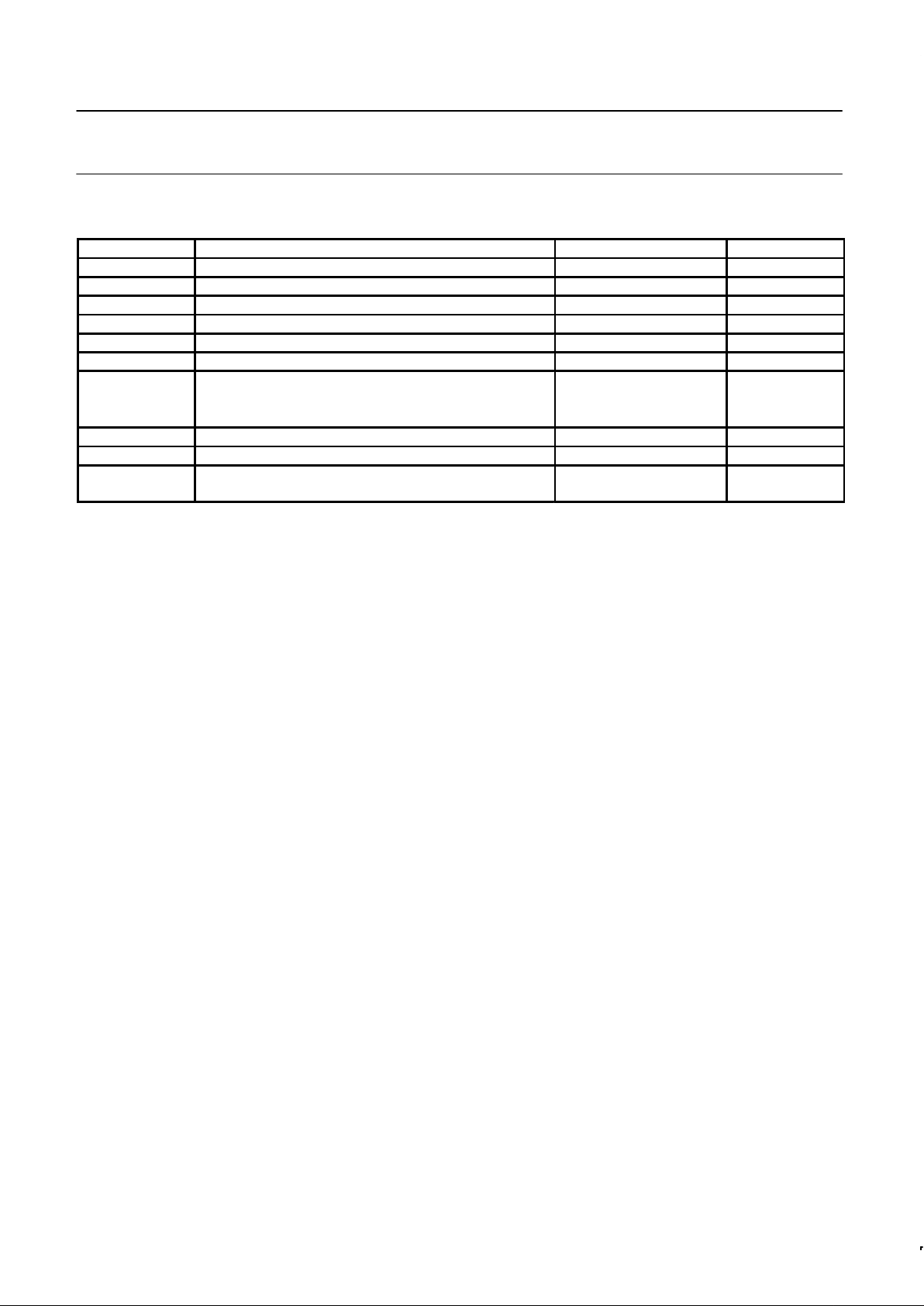
ABSOLUTE MAXIMUM RATINGS


SYMBOL

PARAMETER

RATING

UNIT


V1+

Positive supply voltage


+15

V

V1-

Negative supply voltage


-15

V

V2+

Gate supply voltage


+7

V

VOUT

Output voltage


+7

V

VIN

Differential input voltage


±5

V

VCM

Input common mode voltage


±6

V

P

D

Maximum power dissipation1

T =25°C (still-air)


A


N package


1420

mW


D package


1040

mW


TA

Operating temperature range


0 to +70

°C

TSTG

Storage temperature range


-65 to +150

°C

TSOLD

Lead soldering temperature


(10 sec max)


+300

°C

NOTES:

1. Derate above 25°C at the following rates: N package at 11.5mW/°C

D package at 8.3mW/°C

August 31, 1994

321

Loading...
+ 3 hidden pages