

Philips NE527N Datasheet
Philips Semiconductors Linear Products Product specification
NE527Voltage comparator
315
August 31, 1994 853-0906 13721
DESCRIPTION
The NE527 is a high-speed analog voltage comparator which, for
the first time, mates state-of-the-art Schottky diode technology with
the conventional linear process. This allows simultaneous
fabrication of high speed TTL gates with a precision linear amplifier
on a single monolithic chip. The NE527 is similar in design to the
Philips Semiconductors NE529 voltage comparator except that it
incorporates an “Emitter-Follower” input stage for extremely low
input currents. This opens the door to a whole new range of
applications for analog voltage comparators.
FEATURES
•15ns propagation delay
•Complementary output gates
•TTL or ECL compatible outputs
•Wide common-mode and differential voltage range
•Typical gain of 5000
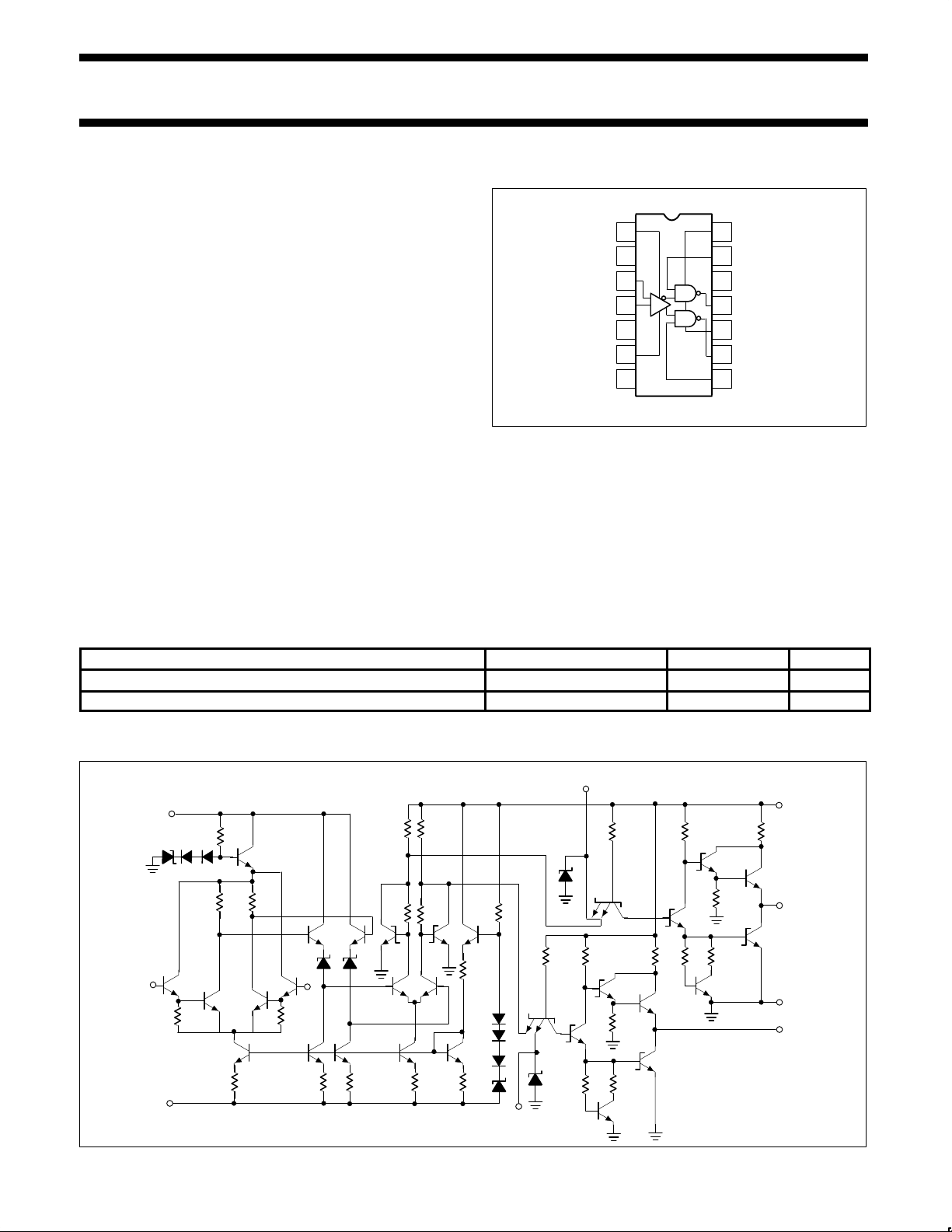
PIN CONFIGURATIONS
1
2
3
4
5
6
7 8
14
13
12
11
10
9
V1
+
NC
INPUT A
INPUT B
NC
V1
–
NC
V2
+
STROBE A
OUTPUT A
NC
GND
OUTPUT B
STROBE B
D, N Packages
TOP VIEW
APPLICATIONS
•A/D conversion
•ECL-to-TTL interface
•TTL-to-ECL interface
•Memory sensing
•Optical data coupling
ORDERING INFORMATION
DESCRIPTION TEMPERATURE RANGE ORDER CODE DWG #
14-Pin Plastic Dual In-Line Package (DIP) 0 to +70°C NE527N 0405B
14-Pin Small Outline (SO) Package 0 to +70°C NE527D 0175D
EQUIVALENT SCHEMATIC
V
1
20K
1.5K 1.5K
INPUT A
INPUT
B
200
V
1
300300 100 200
750
750
6.13K
1K 1K
STROBE B
20K
4K 1.5K
STROBE A
4K
250 500
4K
55
250
500
GND
OUTPUT B
OUTPUT A
4K
1.5K
V2
+
55
7.5K
–
7.5K
+
Philips Semiconductors Linear Products Product specification
NE527Voltage comparator
August 31, 1994
316
ABSOLUTE MAXIMUM RATINGS
SYMBOL PARAMETER RATING UNIT
V1+ Positive supply voltage +15 V
V1- Negative supply voltage -15 V
V2+ Gate supply voltage +7 V
V
OUT
Output voltage +7 V
V
IN
Differential input voltage ±5 V
V
CM
Input common mode voltage ±6 V
P
D
Max power dissipation
1
25°C ambient (still air)
N package 1420 mW
D package 1040 mW
T
A
Operating temperature range 0 to +70 °C
T
STG
Storage temperature range -65 to +150 °C
T
SOLD
Lead soldering temperature (10sec max) +300 °C
NOTES:
1. Derate above 25°C, at the following rates:
N package 11.4mW/°C
D package 8.3mW/°C
BLOCK DIAGRAM
V
1
+
STROBE A
OUTPUT A
INPUT A
INPUT B
OUTPUT B
STROBE B
V
1
–
V
2
+
 Loading...