

Philips N82S123A, N82S123N, N82S23N Datasheet
Philips Semiconductors Product specification
82S23/82S123256-bit TTL bipolar PROM (32 x 8)
1
November 11, 1986 853-0154 86487
DESCRIPTION
The 82S23 and 82S123 are field
programmable, which means that
custom patterns are immediately
available by following the Signetics
Generic I fusing procedure. The 82S23
and 82S123 devices are supplied with
all outputs at logical Low. Outputs are
programmed to a logic High level at any
specified address by fusing the Ni-Cr
link matrix.
These devices include on-chip decoding
and 1 Chip Enable input for memory
expansion. They feature either Open
Collector or 3-State outputs for
optimization of word expansion in bused
organizations.
Ordering information can be found on
the following page.
The 82S23 and 82S123 devices are
also processed to military requirements
for operation over the military
temperature range. For specifications
and ordering information, consult the
Signetics Military Data Handbook.
FEATURES
•Address access time: 50ns max
•Power dissipation: 1.3mW/bit typ
•Input loading: –100µA max
•On-chip address decoding
•One Chip Enable input
•Output options:
– N82S23: Open Collector
– N82S123: 3-State
•No separate fusing pins
•Unprogrammed outputs are Low level
•Fully TTL compatible
APPLICATIONS
•Prototyping/volume production
•Sequential controllers
•Format conversion
•Hardwired algorithms
•Random logic
•Code conversion
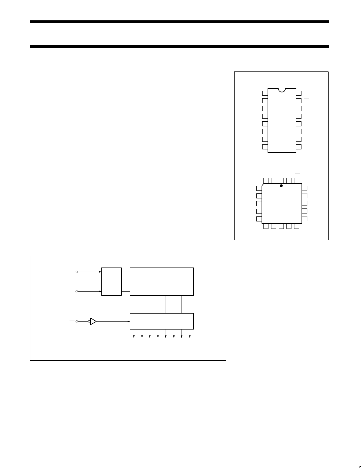
PIN CONFIGURATIONS
1
2
3
4
5
6
7
8 9
10
11
12
13
14
15
16
O1
O2
O3
O4
O5
O6
O7
GND
V
CC
CE
A4
A2
A1
A0
O8
123
4
5
6
7
8
9 10 11 12 13
14
15
16
17
18
1920
A Package
N Package
A3
NC
NCNC
NC
V
CC
CE
A4
A3
A2
A1
A0O8GNDO7
O5
O6
O3
O4
O2
O1
BLOCK DIAGRAM
O2 O4 O6 O8
A0
A4
CE
ADDRESS
LINES
1:32
DECODER
32 × 8 MATRIX
8 OUTPUT DRIVERS
OUTPUT LINES
O1 O3 O5 O7

Philips Semiconductors Product specification
82S23/82S123256-bit TTL bipolar PROM (32 x 8)
November 11, 1986
2
ORDERING INFORMATION
DESCRIPTION ORDER CODE
16-Pin Plastic Dual-In-Line
300mil-wide
N82S23 N, N82S123 N
20-Pin Plastic Leaded Chip Carrier
350mil-square
N82S23 A, N82S123 A
ABSOLUTE MAXIMUM RATINGS
SYMBOL PARAMETER RATING UNIT
V
CC
Supply voltage +7.0 V
DC
V
IN
Input voltage +5.5 V
DC
V
OH
Output voltage High (82S23) +5.5 V
DC
V
O
Output voltage Off-State (82S123) +5.5 V
DC
T
amb
Operating temperature range 0 to +75 °C
T
stg
Storage temperature range –65 to +150 °C
DC ELECTRICAL CHARACTERISTICS
0°C ≤ T
amb
≤ +75°C, 4.75V ≤ VCC ≤ 5.25V
SYMBOL
PARAMETER TEST CONDITIONS
1, 2
LIMITS UNIT
MIN TYP
3
MAX
Input voltage
V
IL
Low VCC = 4.75V 0.8 V
V
IH
High VCC = 5.25V 2.0 V
V
IC
Clamp IIN = –12mA –1.2 V
Output voltage
CE = Low
V
OL
Low I
OUT
= 16mA 0.45 V
V
OH
High I
OUT
= –2.0mA 2.4 V
Input current
I
IL
Low VIN = 0.45V –100 µA
I
IH
High VIN = 5.5V 50 µA
Output current
I
OLK
Leakage (82S23) CE = High, V
OUT
= 5.5V 40 µA
I
OZ
Hi-Z state (82S123) CE = High, V
OUT
= 5.5V 40 µA
CE = High, V
OUT
= 0.5V –40 µA
I
OS
Short circuit (82S123)
4
CE = Low, V
OUT
= 0V, High stored –15 –90 mA
Supply current
5
I
CC
VCC = 5.25V 96 mA
Capacitance
CE = High, VCC = 5.0V
C
IN
Input VIN = 2.0V 5 pF
C
OUT
Output V
OUT
= 2.0V 8 pF
NOTES:
1. Positive current is defined as into the terminal referenced.
2. All voltages with respect to network ground terminal.
3. Typical values are at V
CC
= 5V, T
amb
= +25°C.
4. Duration of short circuit should not exceed 1 second.
5. Measured with all inputs grounded and all outputs open.
 Loading...