

Philips N74F8960F, N74F8961N, N74F8961F, N74F8961A, N74F8960N Datasheet
Philips Semiconductors FAST Products Product specification
74F8960/74F8961
Octal latched bidirectional Futurebus transceivers
(3-State + open-collector)
1
December 19, 1990 853-1120 01322
FEATURES
•Octal latched transceiver
•Drives heavily loaded backplanes with
equivalent load impedances down to 10Ω
•High drive (100mA) open collector drivers
on B port
•Reduced voltage swing (1 volt) produces
less noise and reduces power consumption
•High speed operation enhances
performance of backplane buses and
facilitates incident wave switching
•Compatible with IEEE futurebus standards
•Built-in precision band-gap reference
provides accurate receiver thresholds and
improved noise immunity
•Controlled output ramp and multiple GND
pins minimize ground bounce
•Glitch-free power up/down operation
DESCRIPTION
The 74F8960 and 74F8961 are octal
bidirectional latched transceivers and are
intended to provide the electrical interface to
a high performance wired–OR bus. The B
port inverting drivers are low–capacitance
open collector with controlled ramp and are
designed to sink 100mA from 2 volts. The B
port inverting receivers have a 100 mV
threshold region and a 4ns glitch filter.
The B port interfaces to ‘Backplane
Transceiver Logic’ (BTL). BTL features a
reduced (1V to 2V) voltage swing for lower
power consumption and a series diode on
the drivers to reduce capacitive loading.
Incident switching is employed, therefore BTL
propagation delays are short. Although the
voltage swing is much less for BTL, so is its
receiver threshold region, therefore noise
margins are excellent.
BTL offers low power consumption, low
ground bounce, EMI and crosstalk, low
capacitive loading, superior noise margin and
low propagation delays. This results in a high
bandwidth, reliable backplane.
The 74F8960 and 74F8961 A ports have TTL
3–state drivers and TTL receivers with a latch
function. A separate High–level control input
(VX) is provided to limit the A side output
level to a given voltage level (such as 3.3V).
For 5.0V systems, VX is simply tied to VCC.
The 74F8961 is the non–inverting version of
74F8960.
TYPE
TYPICAL PROPAGATION DELAY TYPICAL SUPPLY CURRENT( TOTAL)
74F8960 6.5ns 80mA
74F8961 6.5ns 80mA
ORDERING INFORMATION
ORDER CODE
DESCRIPTION COMMERCIAL RANGE
V
CC
= 5V ±10%, T
amb
= 0°C to +70°C
28–pin plastic DIP (300 mil)
1
N74F8960N, N748961N
28–pin PLCC
1
N74F8960A, N74F8961A
NOTE: Thermal mounting techiques are recommended.
INPUT AND OUTPUT LOADING AND FAN OUT TABLE
PINS DESCRIPTION
74F (U.L.)
HIGH/LOW
LOAD VALUE
HIGH/LOW
A0 – A8 PNP latched inputs 3.5/0.117 70µA/70µA
B0 – B8 Data inputs with threshold circuitry 5.0/0.167 100µA/100µA
OEA A output enable input (active high) 1.0/0.033 20µA/20µA
OEB0, OEB1 B output enable inputs (active low) 1.0/0.033 20µA/20µA
LE Latch enable input (active low) 1.0/0.033 20µA/20µA
A0 – A7 3–state outputs 150/40 3mA/24mA
B0 – B7 Open collector outputs OC/166.7 OC/100mA
NOTES:
1. One (1.0) FAST unit load is defined as: 20µA in the high state and 0.6mA in the low state.
2. OC = Open collector.

Philips Semiconductors FAST Products Product specification
74F8960/74F8961
Octal latched bidirectional Futurebus transceivers
(3-State + open-collector)
December 19, 1990
2
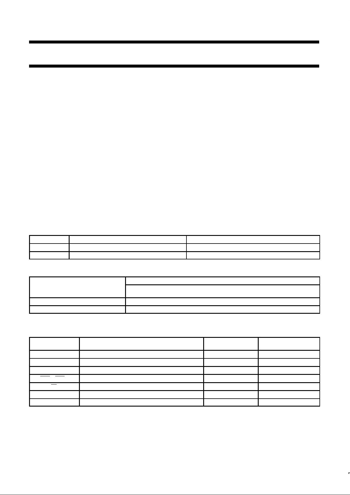
PIN CONFIGURATION PIN CONFIGURATION PLCC LOGIC SYMBOL
1
2
3
4
5
6
7
8
9
10 19
20
21
22
23
24
25
26
27
28
OEA
A1
GND
A3
A4
V
CC
15
2
28
16
A0
V
X
OEB1
OEB
0
OEB1
OEB0
OEA
LE
3 5 6
A0 A1 A2
GND
A5
4 3 2 1 28 27
25
24
23
22
21
20
11
10
9
8
7
6
18
16 17151413
26
19
12
5
PLCC
A1
A2
A3
GND
A4
11
12
13
14 15
16
17
18
A2
GND
A5
A6
GND
A7
B0
B2
GND
GND
B5
LE
B1
B3
B4
B6
B7
GND
V
CC
OEAA0GND LE B0 B1
GND
B2
B3
GND
B5
B4
B6
GNDOEB
1OEB2 B7
V
X
A7A6
7 9 10 12 13
A6 A7A3 A4 A5
27 26 24
B0 B1 B2
23 21 20 19 17
B6 B7B3 B4 B5
V
CC
= Pin 1, V
X
= Pin 14
GND = Pin 4, 8, 11, 18, 22, 25
74F8960
74F8960 74F8960
PIN CONFIGURATION PIN CONFIGURATION PLCC LOGIC SYMBOL
15
2
28
16 OEB1
OEB0
OEA
LE
3 5 6
A0 A1 A2
7 9 10 12 13
A6 A7A3 A4 A5
27 26 24
B0 B1 B2
23 21 20 19 17
B6 B7B3 B4 B5
V
CC
= Pin 1, V
X
= Pin 14
GND = Pin 4, 8, 11, 18, 22, 25
74F8961
74F8961 74F8961
1
2
3
4
5
6
7
8
9
10 19
20
21
22
23
24
25
26
27
28
OEA
A1
GND
A3
A4
V
CC
A0
V
X
OEB1
OEB
0
11
12
13
14 15
16
17
18
A2
GND
A5
A6
GND
A7
B0
B2
GND
GND
B5
LE
B1
B3
B4
B6
B7
GND
GND
A5
4 3 2 1 28 27
25
24
23
22
21
20
11
10
9
8
7
6
18
16 17151413
26
19
12
5
PLCC
A1
A2
A3
GND
A4
V
CC
OEAA0GND LE B0 B1
GND
B2
B3
GND
B5
B4
B6
GNDOEB
1OEB2 B7
V
X
A7A6
Philips Semiconductors FAST Products Product specification
74F8960/74F8961
Octal latched bidirectional Futurebus transceivers
(3-State + open-collector)
December 19, 1990
3
IEC/IEEE SYMBOL FOR 74F8960 IEC/IEEE SYMBOL FOR 74F8961
74F8960 74F8961
3
2
3
&
EN2
EN3
C1
1D
27
26
24
23
21
20
19
17
5
6
7
9
10
11
13
15
16
28
2
3
2
3
&
EN2
EN3
C1
1D
27
26
24
23
21
20
19
17
5
6
7
9
10
11
13
15
16
28
2
PIN DESCRIPTION
SYMBOL PINS TYPE NAME AND FUNCTION
A0 – A7 3, 5, 6, 7, 9, 10, 12, 13 I/O PNP latched input/3–state output (with VX control option)
B0 – B7 27, 26, 24, 23, 21, 20, 19, 17 I/O
Data input with special threshold circuitry to reject noise/ open collector output, high
current drive
OEB0 15 Input Enables the B outputs when both pins are low
OEB1 16 Input Enables the A outputs when high
LE 28 Input Latched when high (a special feature is buillt in for proper enabling times)
V
X
14 Input Clamping voltage keeping VOH from rising above VX (VX = Vcc for normal use)
Philips Semiconductors FAST Products Product specification
74F8960/74F8961
Octal latched bidirectional Futurebus transceivers
(3-State + open-collector)
December 19, 1990
4
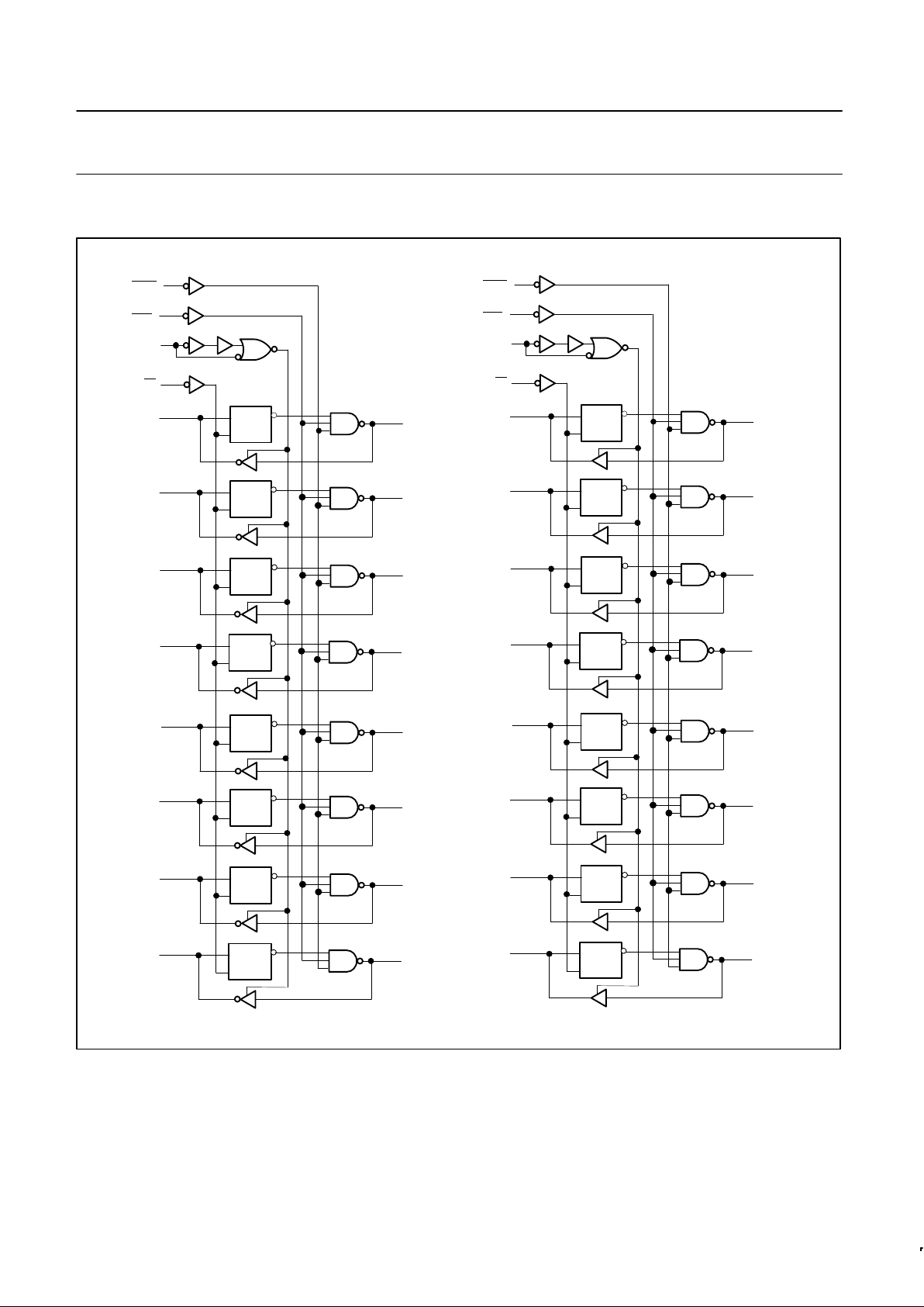
LOGIC DIAGRAM
LE
B0
OEB0
Data
Q
27
3
LE
OEA
V
CC
= Pin 1, V
X
= Pin 14,
GND = Pin 4, 8, 11, 18, 22, 25
A0
LE
B1
Data
Q
26
5
A1
LE
B2
Data
Q
24
6
A2
LE
B3
Data
Q
23
7
A3
LE
B4
Data
Q
21
9
A4
LE
B5
Data
Q
20
10
A5
LE
B6
Data
Q
19
12
A6
LE
B7
Data
Q
17
13
A7
28
2
16
15
OEB
1
LE
B0
OEB0
Data
Q
27
3
LE
OEA
A0
LE
B1
Data
Q
26
5
A1
LE
B2
Data
Q
24
6
A2
LE
B3
Data
Q
23
7
A3
LE
B4
Data
Q
21
9
A4
LE
B5
Data
Q
20
10
A5
LE
B6
Data
Q
19
12
A6
LE
B7
Data
Q
17
13
A7
28
2
16
15
OEB1
74F9861
74F9860
 Loading...