

Philips N74F786N, N74F786D Datasheet

INTEGRATED CIRCUITS
74F786
4-bit asynchronous bus arbiter
Product specification
IC15 Data Handbook
1991 Feb 14
Philips Semiconductors Product specification
74F7864-bit asynchronous bus arbiter
FEA TURES
•Arbitrates between 4 asynchronous inputs
•Separate grant output for each input
•Common output enable
•On board 4 input AND gate
•Metastable–free outputs
•Industrial temperature range available (–40°C to +85°C)
The 74F786 is designed so that contention between two or more
request signals will not glitch or display a metastable condition. In
this situation an increase in the BR
n to BGn t
may be observed.
PHL
A typical 74F786 has an h = 6.6ns, t = 0.41ns and To = 5µsec.
Where:
h = Typical propagation delay through the device and t and To are
device parameters derived from test results and can most nearly be
defined as:
t = A function of the rate at which a latch in a metastable state
resolves that condition.
DESCRIPTION
The 74F786 is an asynchronous 4–bit arbiter designed for high
speed real–time applications. The priority of arbitration is determined
on a first–come first–served basis. Separate bus grant (BGn)
outputs are available to indicate which one of the request inputs is
served by the arbitration logic. All BG
common enable (EN
) pin. In order to generate a bus request signal
a separate 4 input AND gate is provided which may also be used as
an independent AND gate. Unused bus request (BR
disabled by tying them high.
n outputs are enabled by a
) inputs may be
To = A function of the measurement of the propensity of a latch to
enter a metastable state. To is also a very strong function of the
normal propagation delay of the device.
For further information, please refer to the 74F786 application notes.
TYPE
TYPICAL
PROPAGATION DELAY
TYPICAL
SUPPLY CURRENT
74F786 6.6ns 55mA
ORDERING INFORMATION
ORDER CODE
COMMERCIAL RANGE INDUSTRIAL RANGE
DESCRIPTION VCC = 5V ±10%, VCC = 5V ±10%, PKG DWG #
T
= 0°C to +70°C T
amb
16–pin plastic DIP N74F786N I74F786N SOT 38-4
16–pin plastic SO N74F786D I74F786D SOT109-1
= –40°C to +85°C
amb
(TOTAL)
INPUT AND OUTPUT LOADING AND FAN OUT TABLE
PINS
BR0 – BR3
A, B, C, D
EN
YOUT
BG0 – BG3
Bus request inputs (active low)
AND gate inputs
Common bus grant output enable input (active low)
AND gate output
Bus grant outputs (active low)
NOTE:
One (1.0) FAST unit load is defined as: 20µA in the high state and 0.6mA in the low state.
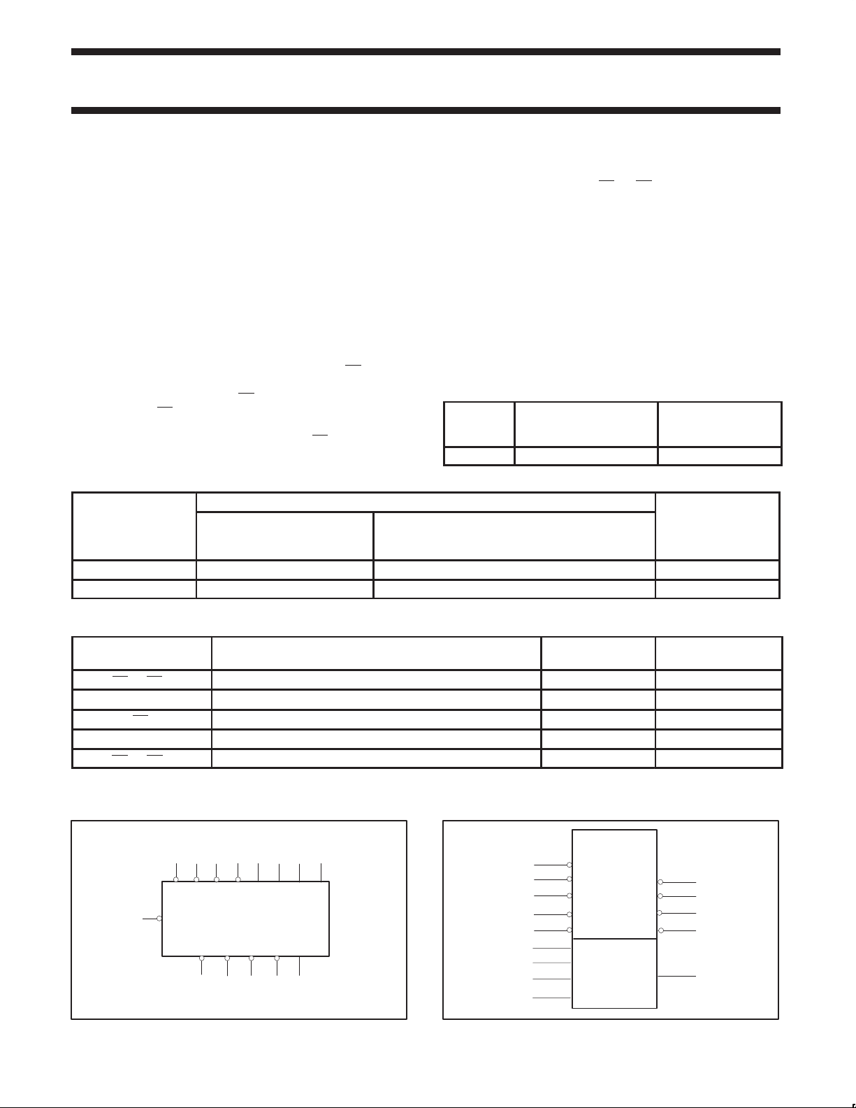
LOGIC SYMBOL
456715123
BR0 BR1 BR2 BR3 A B C D
EN
6
BG0 BG1 BG2 BG3 YOUT
13 12 11 10 14
V
= Pin 16
CC
GND = Pin 8
SF00442
DESCRIPTION
IEC/IEEE SYMBOL
74F (U.L.) HIGH/
1.0/3.0
1.0/1.0
1.0/1.0
150/40
150/40
9
4
5
6
7
15
1
2
3
EN
BR0
BR1
BR2
BR3
LOW
BUS ARBITER
Φ
74F786
&
LOAD VALUE HIGH/
20µA/1.8mA
20µA/0.6mA
20µA/0.6mA
3.0mA/24mA
3.0mA/24mA
BG0
BG1
BG2
BG3
13
12
11
10
14
SF00443
LOW
February 14, 1991 853–1269 01717
2
Philips Semiconductors Product specification
74F7864-bit asynchronous bus arbiter
FUNCTIONAL DESCRIPTION
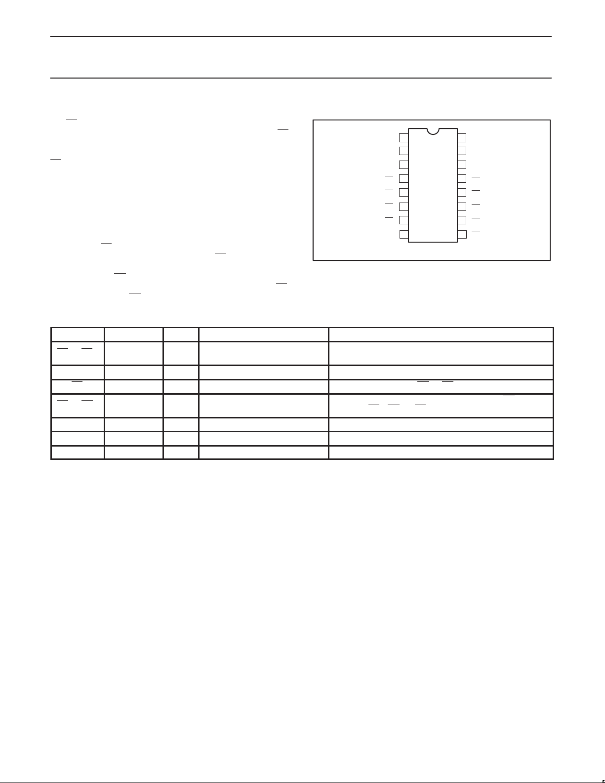
PIN CONFIGURATION
The BRn inputs have no inherent priority. The arbiter assigns priority
to the incoming requests as they are received, therefore, the first BR
asserted will have the highest priority. When a bus request is
received its corresponding bus grant becomes active, provided that
EN
is low. If additional bus requests are made during this time they
are queued. When the first request is removed, the arbiter services
the bus request with the next highest priority. Removing a request
while a previous request is being serviced can cause a grant to be
changed when arbitrating between three or four requests. For that
reason, the user should not remove ungranted requests when
arbitrating between three or four requests. This does not apply to
arbitration between two requests.
If two or more BR
one of them will be selected at random, and all BG
n inputs are asserted at precisely the same time,
n outputs will be
BR
BR
BR
BR3
GND
1
B
2
C
3
D
4
0
5
1
6
2
held in the high state until the selection is made. This guarantees
that an erroneous BG
n will not be generated even though a
metastable condition may occur internal to the device. When the EN
is in the high state the BGn outputs are forced high.
PIN DESCRIPTION
SYMBOL PINS TYPE NAME FUNCTION
BR0 – BR3 4, 5, 6, 7 Input Bus request inputs (active low)
A, B, C, D 15, 1, 2, 3 Input Inputs of the 4–input AND gate
EN 9 Input Enable input When low it enables the BG0 – BG3 outputs.
BG0 – BG3 13, 12, 11, 10 Output Bus grant outputs (active low)
YOUT 14 Output Output of the 4–input AND gate
GND 8 Ground ground (0V)
V
CC
16 Power Positive supply voltages
The logic of this device arbitrates between these four inputs.
Unused inputs should be tied high.
These outputs indicate the selected bus request. BG0 corresponds to BR0, BG1 to BR1, etc.
16
V
CC
15
A
14
YOUT
13
BG
12
BG1
11
BG
107
BG
98
EN
SF00441
0
2
3
February 14, 1991
3
Philips Semiconductors Product specification
74F7864-bit asynchronous bus arbiter
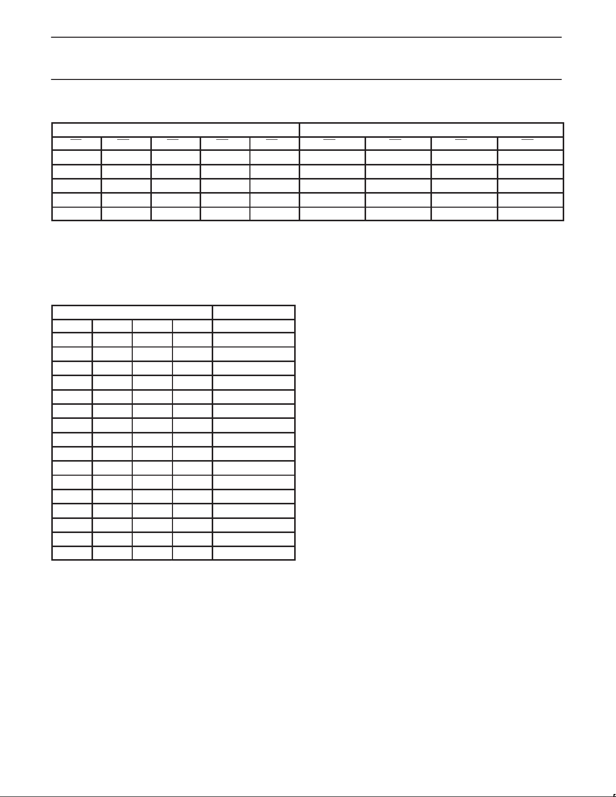
ARBITER FUNCTION TABLE
INPUTS OUTPUTS
EN BR0 BR1 BR2 BR3 BG0 BG1 BG2 BG3
L 1 X X X L H H H
L X 1 X X H L H H
L X X 1 X H H L H
L X X X 1 H H H L
H X X X X H H H H
Notes to mode selection function table
H = High–voltage level
L = Low–voltage level
X = Don’t care
1 = First of inputs to go low
ARBITER FUNCTION TABLE
INPUTS OUTPUT
A B C D YOUT
L L L L L
L L L H L
L L H L L
L L H H L
L H L L L
L H L H L
L H H L L
L H H H L
H L L L L
H L L H L
H L H L L
H L H H L
H H L L L
H H L H L
H H H L L
H H H H H
Notes to AND function table
H = High–voltage level
L = Low–voltage level
February 14, 1991
4
 Loading...