

Philips N74F657D, N74F657DB, N74F657N Datasheet
INTEGRATED CIRCUITS
74F657
Octal transceiver with 8-bit parit
generator/checker
Process specification
IC15 Data Handbook
1990 Jul 30
Philips Semiconductors Product specification
74F657Octal transceiver with 8-bit parity generator/checker
FEA TURES
• Combines 74F245 and 74F280A functions in one package
• High impedance base input for reduced loading (70µA in
high and low states)
• Ideal in applications where high output drive and light bus
loading are required (I
is 70µA vs FAST std of 600µA)
IL
• 3–state buffer outputs sink 64mA and source 15mA
• Input diodes for termination effects
• 24–pin plastic slim DIP (300mil) package
• Industrial temperature range available (–40°C to +85°C)
DESCRIPTION
The 74F657 is an octal transceiver featuring non–inverting
buffers with 3–state outputs and an 8–bit parity
generator/checker, and is intended for bus–oriented
applications. The buffers have a guaranteed current sinking
capability of 24mA at the A ports and 64mA at the B ports.
The transmit/receive (T/R
the data flow through the bidirectional transceivers.
Transmit (active high) enables data from A ports to B ports;
receive (active low) enables data from B ports to A ports.
The output enable (OE) input disables both the A and B ports by
placing them in a high impedance condition when the OE
.
high
) input determines the direction of
input is
The parity select (ODD/EVEN) input gives the user the option of
odd or even parity systems
The parity (PARITY) pin is an output from the generator/checker
when transmitting from the port A to B (T/R
when receiving from port B to A port ( T/R
When transmitting (T/R
is set, then the A port data is polled to determined the number of
high bits. The parity (PARITY) output then goes to the logic state
determined by the parity select (ODD/EVEN
number of high bits on port A.
For example, if the parity select (ODD/EVEN
parity), and the number of high bits on port A is odd, then the parity
(PARITY) output will be high, transmitting even parity. If the number
of high bits on port A is even, then the parity (PARITY) output will
be low, keeping even parity.
When in receive mode (T/R
the number of high bits. If parity select (ODD/EVEN
parity) and the number of highs on port B is:
(1) odd and the parity (PARITY) input is high, then ERROR
high, significantly no error.
(2) even and the parity (PARITY) input is high, then ERROR
asserted low, indicating an error.
TYPE
74F657 8.0ns 100mA
TYPICAL PROPAGA-
TION DELAY
.
= high) and an input
= low).
= high) the parity select (ODD/EVEN) input
) setting and by the
) is set low (even
= low) the B port is polled to determine
) is low (even
will be
will be
TYPICAL SUPPL Y
CURRENT( TOTAL)
ORDERING INFORMATION
ORDER CODE
COMMERCIAL RANGE INDUSTRIAL RANGE
DESCRIPTION
24–pin plastic slim
DIP (300mil)
24–pin plastic SOL N74F657D I74F657D SOT137-1
24–pin plastic SSOP N74F657DB I74F657DB SOT340-1
VCC = 5V ±10%, VCC = 5V ±10%,
T
= 0°C to +70°C T
amb
N74F657N I74F657N SOT222-1
= –40°C to +85°C
amb
PKG DWG #
INPUT AND OUTPUT LOADING AND FAN OUT TABLE
PINS DESCRIPTION
A0 – A7 A ports 3–state inputs 3.5/0.1 17
B0 – B7 B ports 3–state inputs 3.5/0.1 17
PARITY Parity input 3.5/0.1 17
T/R Transmit/receive input 2.0/0.066
ODD/EVEN Parity select input 1.0/0.033
OE Output enable input (active low) 2.0/0.066
A0 – A7 A ports 3–state outputs 150/40 3.0mA/24mA
B0 – B7 B ports 3–state outputs 750/106.7 15mA/64mA
PARITY Parity output 750/106.7 15mA/64mA
ERROR Error output 750/106.7
Note to input and output loading and fan out table
1. One (1.0) FAST unit load is defined as: 20µA in the high state and 0.6mA in the low state.
74F (U.L.)
HIGH/LOW
LOAD VALUE
HIGH/LOW
70µA/70µA
70µA/70µA
70µA/70µA
40µA/40µA
20µA/20µA
40µA/40µA
15mA/64mA
90 July 30 853 1117 00081
2
Philips Semiconductors Product specification
74F657Octal transceiver with 8-bit parity generator/checker
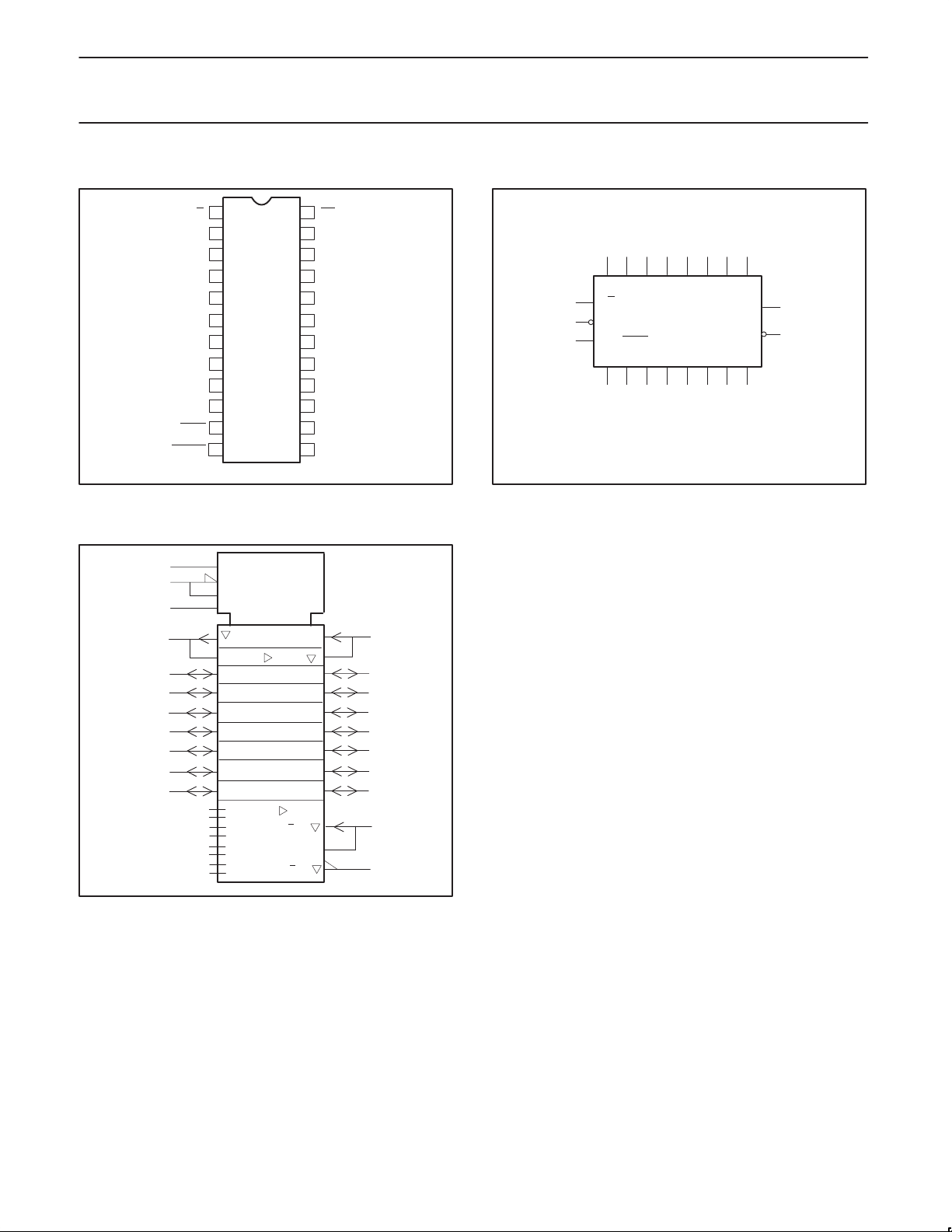
PIN CONFIGURATION
T/R
1OE
2
A0
3
A1
4
A2
5
A3
6
A4
V
7
CC
A5
8
A6
9
A7
10
ODD/EVEN
11
ERROR
IEC/IEEE SYMBOL
24
1
11
2
3
4
5
6
8
9
10
3 EN1/3G5 (REC)
3 EN2 (XMIT)
N4
Z11
G3
LOGIC SYMBOL
24
23
B0
22
B1
21
B2
20
B3
GND
19
GND
18
17
B4
16
B5
15
B6
14
B7
PARITY
1312
SF00414
5
23
22
21
20
17
16
15
14
13
12
SF00416
1
2
11
2 k
.
.
.
18
4, 2
4, 1
= Pin 7
V
CC
GND = Pin 18, 19
234568910
A0 A1 A2 A3 A4 A5 A6 A7
T/R
1
OE
24
ODD/EVEN
11
B0 B1 B2 B3
23 22 21 20 17 16 15 14
PARITY
ERROR
B4 B5 B6 B7
13
12
SF00415
90 July 30
3
Philips Semiconductors Product specification
74F657Octal transceiver with 8-bit parity generator/checker
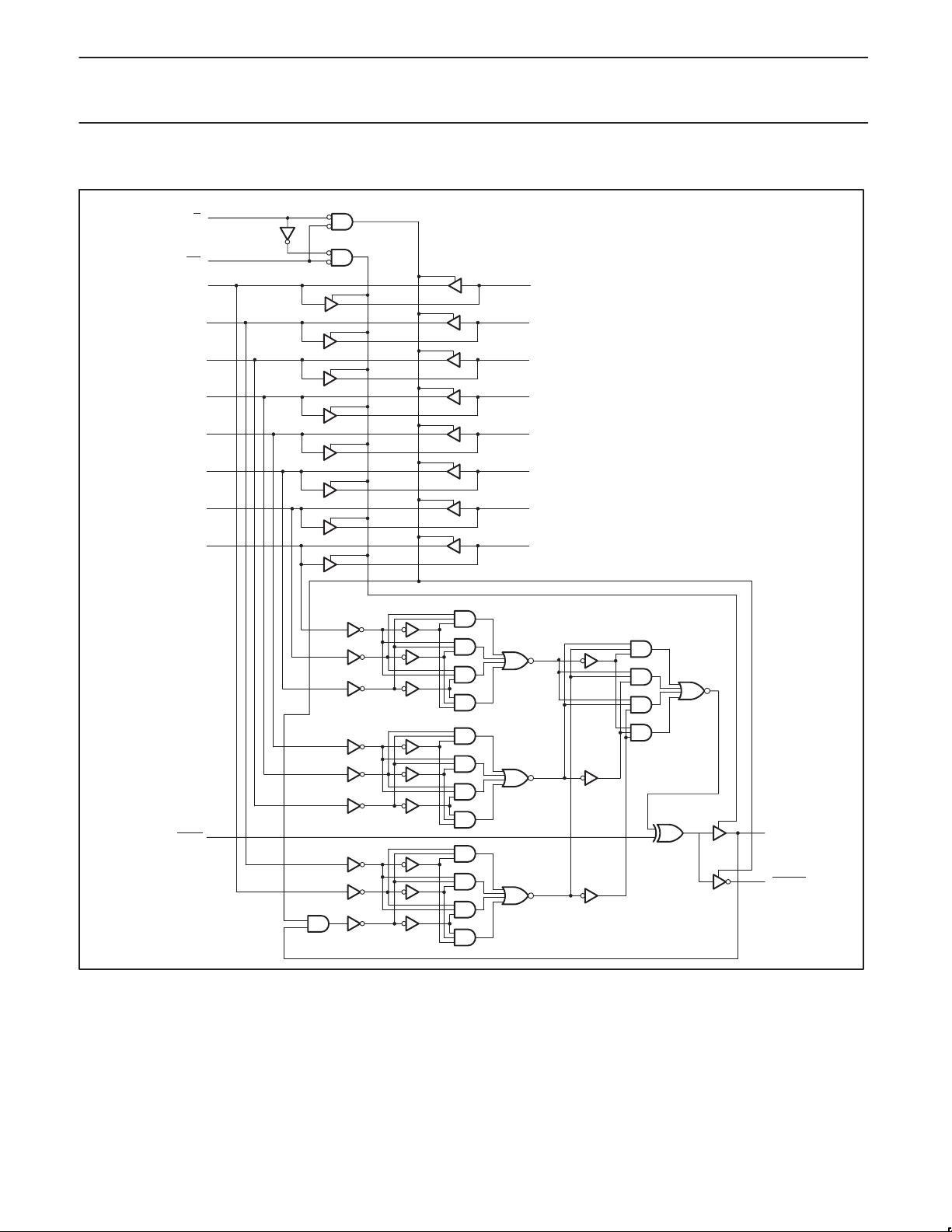
LOGIC DIAGRAM
1
T/R
24
OE
2
A0
23
B0
3
A1
4
A2
5
A3
6
A4
8
A5
9
A6
10
A7
22
B1
21
B2
20
B3
17
B4
16
B5
15
B6
14
B7
VCC = Pin 7,
GND = Pin 18, 19
90 July 30
ODD/EVEN
11
13
12
PARITY
ERROR
SF00417
4
 Loading...