

Philips N74ALS563AD, N74ALS563AN, N74ALS564AD Datasheet

74ALS563A/74ALS564A
Latch flip/flop
Product specification
IC05 Data Handbook
1996 Jul 01
INTEGRATED CIRCUITS
Philips Semiconductors Product specification
74ALS563A/74ALS564ALatch/flip-flop
74ALS563A Octal transparent latch, inverting (3-State)
74ALS564A Octal D flip-flop, inverting (3-State)
2
1996 Jul 01 853–1306 01670
FEA TURES
•74ALS563A is broadside pinout and inverting version of
74ALS373
•74ALS564A is broadside pinout and inverting version of
74ALS374
•Inputs and outputs on opposite side of package allow easy
interface to microprocessors
•Useful as an input or output port for microprocessors
•3-State outputs for bus interfacing
•Common output enable
•74ALS573A and 74ALS574A are non-inverting version of
74ALS563B and 74ALS564A respectively
TYPE
TYPICAL
PROPAGATION DELAY
TYPICAL
SUPPLY CURRENT
(TOTAL)
74ALS563A 6.0ns 12mA
74ALS564A 6.0ns 15mA
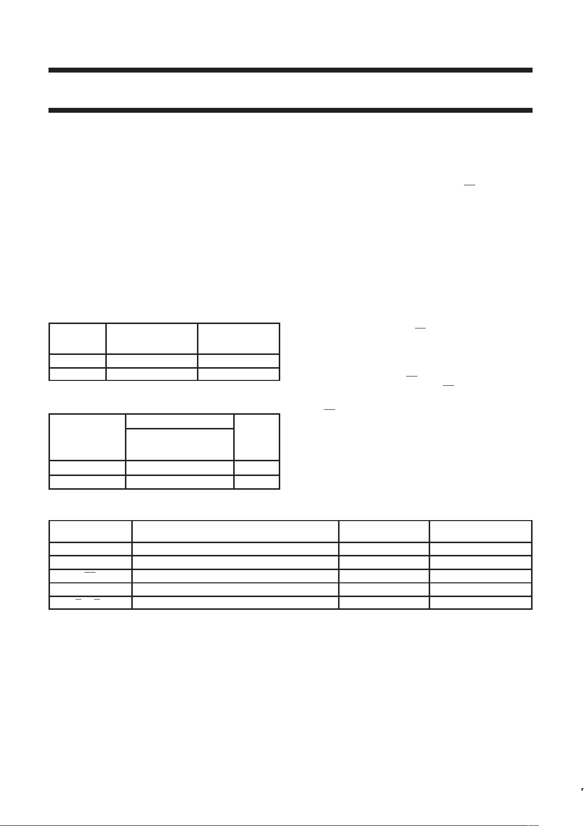
ORDERING INFORMATION
ORDER CODE
DESCRIPTION COMMERCIAL RANGE
V
CC
= 5V ±10%,
T
amb
= 0°C to +70°C
DRAWING
NUMBER
20-pin plastic DIP 74ALS563AN, 74ALS564AN SOT146-1
20-pin plastic SOL 74ALS563AD, 74ALS564AD SOT163-1
DESCRIPTION
The 74ALS563A is an octal transparent latch coupled to eight
3-State output devices. The two sections of the device are controlled
independently by enable (E) and output enable (OE
) control gates.
The 74ALS563A is a complementary version of the 74ALS373 and
has a broadside pinout configuration to facilitate PC board layout
and allow easy interface with microprocessors.
The data on the D inputs is transferred to the latch outputs when the
enable (E) input is High. The latch remains transparent to the data
input while E is High, and stores the inverted data that is present
one setup time before the High-to-Low enable transition.
The 74ALS564A is a complementary version of the 74ALS373 and
has a broadside pinout configuration to facilitate PC board layout
and allow easy interface with microprocessors.
It is an 8-bit edge triggered register coupled to eight 3-State output
buffers. The two sections of the device are controlled independently
by clock (CP) and output enable (OE
) control gates.
The register is fully edge triggered. The state of the D input, one
setup time before the Low-to-High clock transition is transferred to
the corresponding flip-flop’s Q output.
The active-Low output enable (OE
) controls all eight 3-State buffers
independent of the latch operation. When OE
is Low, latched or
transparent data appears at the output.
When OE
is High, the outputs are in high impedance “off” state,
which means they will neither drive nor load the bus.
INPUT AND OUTPUT LOADING AND FAN-OUT TABLE
PINS DESCRIPTION
74ALS (U.L.)
HIGH/LOW
LOAD VALUE
HIGH/LOW
D0 – D7 Data inputs 1.0/2.0 20µA/0.2mA
E (74ALS563A) Enable input 1.0/1.0 20µA/0.1mA
OE Output enable input (active-Low) 1.0/1.0 20µA/0.1mA
CP (74ALS564A) Clock pulse input (active rising edge) 1.0/2.0 20µA/0.2mA
Q0 – Q7 Data outputs 130/240 2.6mA/24mA
NOTE: One (1.0) ALS unit load is defined as: 20µA in the High state and 0.1mA in the Low state.
Philips Semiconductors Product specification
74ALS563A/74ALS564ALatch/flip-flop
1996 Jul 01
3
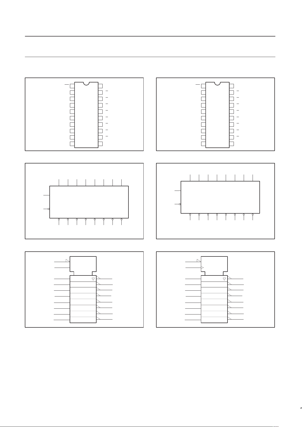
PIN CONFIGURATION – 74ALS563A
1
2
3
4
5
6
7
8
9
10 11
12
13
14
15
16
17
18
19
20
OE
GND
V
CC
E
SC00111
Q0
D0
D1
Q
1
D2
Q2
Q
3
D3
Q
4
D4
Q
5
D5
Q
6
D6
Q
7
D7
PIN CONFIGURATION – 74ALS564A
1
2
3
4
5
6
7
8
9
10 11
12
13
14
15
16
17
18
19
20
OE
GND
V
CC
CP
SF01052
Q0
D0
D1
Q
1
D2
Q2
Q
3
D3
Q
4
D4
Q
5
D5
Q
6
D6
Q
7
D7
LOGIC SYMBOL – 74ALS563A
345678
141516171819
1
11 E
OE
Q0
D0 D1Q1D2
Q2 Q3D3Q4D4Q5
D5
9
2
1213
Q6D6Q7
D7
SC00112
VCC=Pin 20
GND=Pin 10
LOGIC SYMBOL – 74ALS564A
345678
141516171819
1
11 CP
OE
Q0
D0 D1Q1D2
Q2 Q3D3Q4D4Q5
D5
9
2
1213
Q6D6Q7
D7
SF01053
VCC=Pin 20
GND=Pin 10
IEC/IEEE SYMBOL – 74ALS563A
1
2D
EN1
1
SC00113
11
EN2
2
3
4
5
6
7
8
9
19
18
17
16
15
14
13
12
IEC/IEEE SYMBOL – 74ALS564A
1
2D
EN1
1
SF01054
11
C2
2
3
4
5
6
7
8
9
19
18
17
16
15
14
13
12
Philips Semiconductors Product specification
74ALS563A/74ALS564ALatch/flip-flop
1996 Jul 01
4
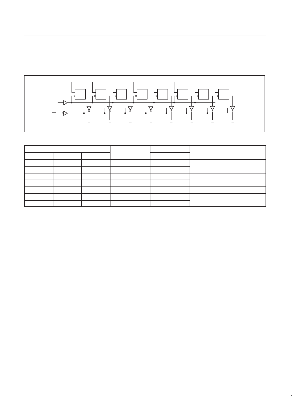
LOGIC DIAGRAM – 74ALS563A
V
CC
= Pin 20
GND = Pin 10
D0
D
E
Q
Q0
2
19
D1
D
E
Q
Q1
3
18
D2
D
E
Q
Q2
4
17
D3
D
E
Q
Q3
5
16
D4
D
E
Q
Q4
6
15
D5
D
E
Q
Q5
7
14
D6
D
E
Q
Q6
8
13
D7
D
E
Q
Q7
9
12
11
E
SC00116
1
OE
FUNCTION T ABLE – 74ALS563A
INPUTS
OUTPUTS
INTERNAL
OE E Dn
REGISTER
Q0 – Q7
OPERATING MODE
L H L L H
L H H H L
Enable and read register
L ↓ l L H
L ↓ h H L
Latch and read register
L L X NC NC Hold
H L X NC Z
p
H H Dn Dn Z
Disable outputs
H = High voltage level
h = High state must be present one setup time before the High-to-Low enable transition
L = Low voltage level
l = Low state must be present one setup time before the High-to-Low enable transition
NC= No change
X = Don’t care
Z = High impedance “off” state
↓ = High-to-Low enable transition
 Loading...