

Philips N74ALS251D, N74ALS251N Datasheet
74ALS251
8–input multiplexer (3–State)
Product specification
IC05 Data Handbook
1991 Feb 08
INTEGRATED CIRCUITS
Philips Semiconductors Product specification
74ALS2518-input multiplexer (3-State)
2
1991 Feb 08 853–1377 01670
FEA TURES
•8-to-1 multiplexing
•On chip decoding
•Multifunction capability
•Inverting and non-inverting outputs
•Both outputs are 3-State for further multiplexer expansion
DESCRIPTION
The 74ALS251 is a logic implementation of a single 8-position
switch with the switch position controlled by the state of three select
(S0, S1, S2) inputs. True (Y) and complementary (Y
) outputs are
both provided.
The output enable (OE
) is active Low. When OE is High, both
outputs are in High impedance state, allowing multiple connections
to a common bus without driving nor loading the bus significantly.
When the outputs of more than one device are tied together, the
user must ensure that there is no overlap in the active-Low portion
of the output enable voltages in order to avoid high currents that
could exceed the maximum current rating.
TYPE
TYPICAL
PROPAGATION DELAY
TYPICAL
SUPPLY CURRENT
(TOTAL)
74ALS251 7.0ns 7.5mA
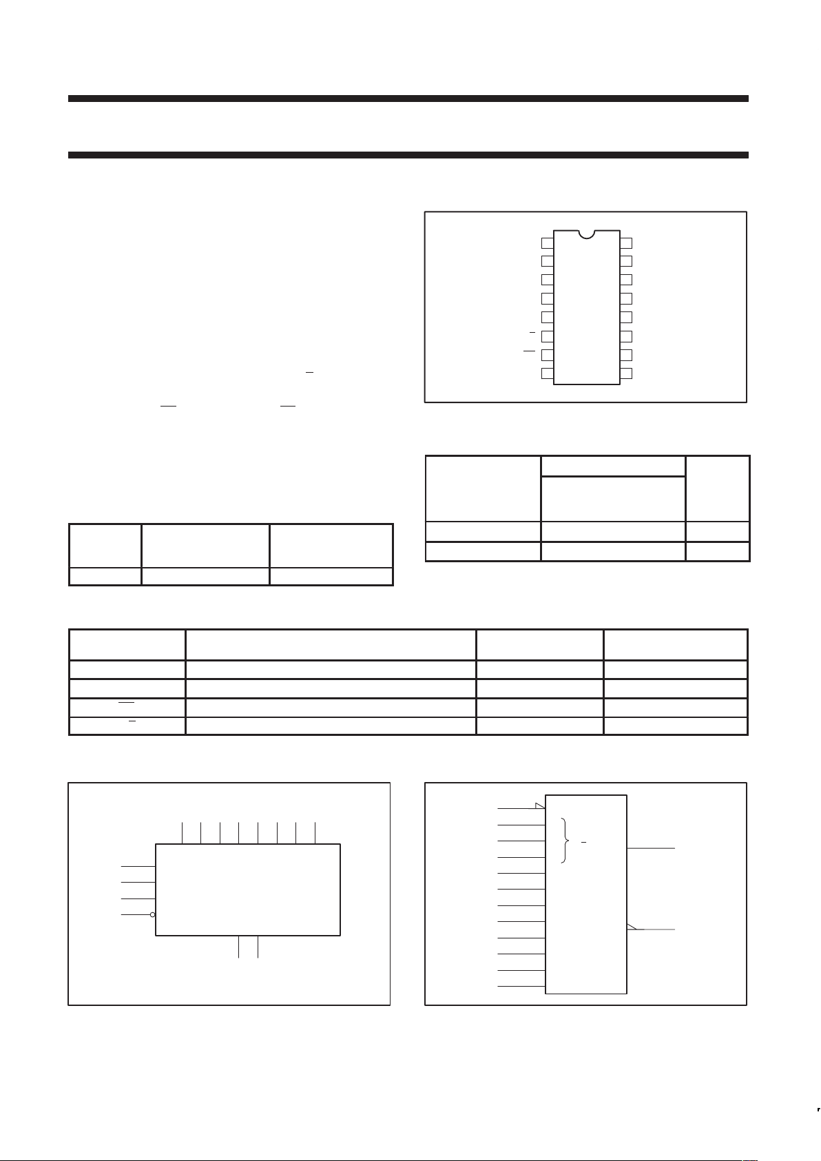
PIN CONFIGURATION
16
15
14
13
12
11
107
6
5
4
3
2
1
OE
V
CC
I7
S0
S1
I6
I4
I5
I3
I2
Y
I1
I0
Y
98GND S2
SC00066
ORDERING INFORMA TION
ORDER CODE
DESCRIPTION COMMERCIAL RANGE
V
CC
= 5V ±10%,
T
amb
= 0°C to +70°C
DRAWING
NUMBER
16-pin plastic DIP 74ALS251N SOT38-4
16-pin plastic SO 74ALS251D SOT109-1
INPUT AND OUTPUT LOADING AND FAN-OUT TABLE
PINS DESCRIPTION
74ALS (U.L.)
HIGH/LOW
LOAD VALUE
HIGH/LOW
I0 – I7 Data inputs 1.0/1.0 20µA/0.1mA
S0 – S2 Select inputs 1.0/1.0 20µA/0.1mA
OE Output Enable input (active-Low) 1.0/1.0 20µA/0.1mA
Y, Y Data outputs 130/240 2.5mA/24mA
NOTE: One (1.0) ALS unit load is defined as: 20µA in the High state and 0.1mA in the Low state.
LOGIC SYMBOL
VCC = Pin 16
GND = Pin 8
SC00067
9
7
S2
OE
4 3 2 1 15 14 13
I0 I1 I2 I3 I4 I5 I6
YY
56
12
I7
10 S1
11 S0
IEC/IEEE SYMBOL
SC00068
MUX
7
11
5
6
0
G
0
7
10
2
9
4
3
2
1
15
14
13
12
EN
Philips Semiconductors Product specification
74ALS2518-input multiplexer (3-State)
1991 Feb 08
3
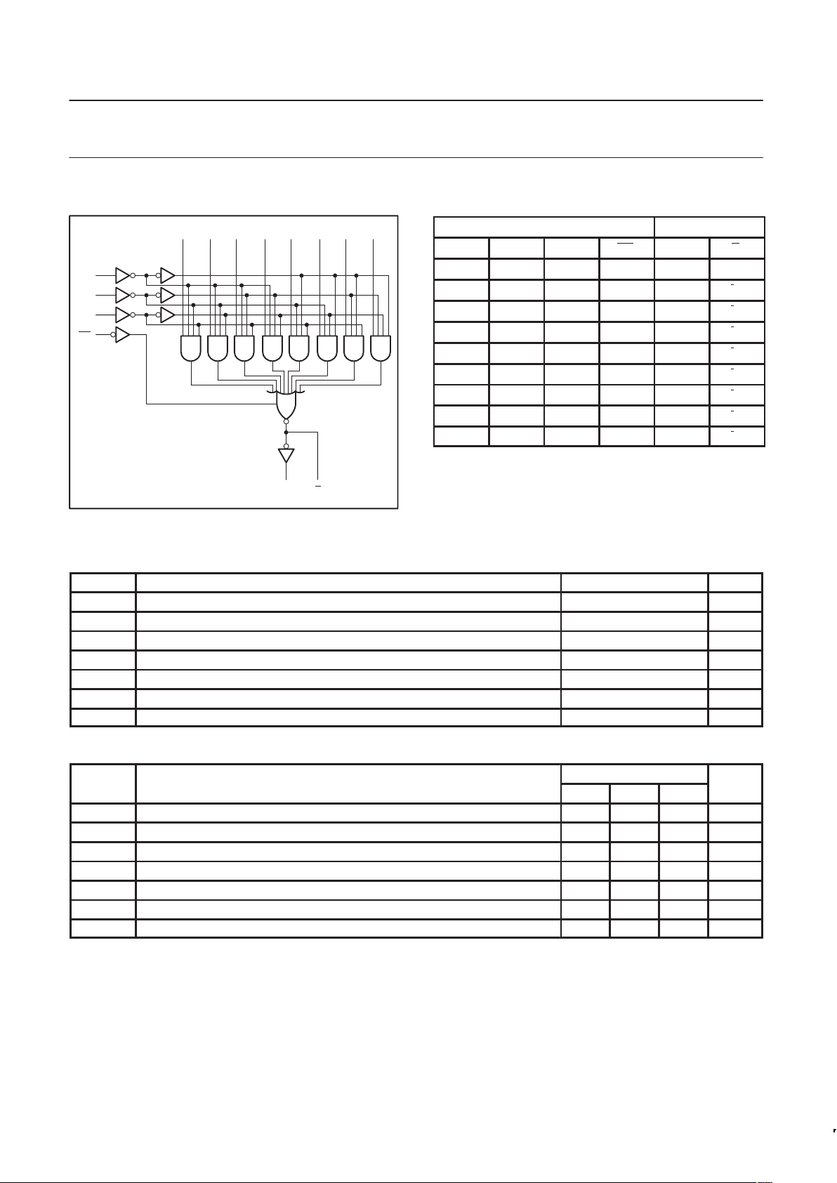
LOGIC DIAGRAM
VCC = Pin 16
GND = Pin 8
SC00069
I0 I1 I2 I3 I4 I5 I6 I7
4 3 2 1 15 14 13 12
S2
S1
S0
OE
9
10
11
7
56
YY
FUNCTION TABLE
INPUTS OUTPUTS
S2 S1 S0 OE Y Y
X X X H Z Z
L L L L I0 I0
L L H L I1 I1
L H L L I2 I2
L H H L I3 I3
H L L L I4 I4
H L H L I5 I5
H H L L I6 I6
H H H L I7 I7
H = High voltage level
L = Low voltage level
X = Don’t care
Z = High impedance “off” state
ABSOLUTE MAXIMUM RATINGS
(Operation beyond the limit set forth in this table may impair the useful life of the device.
Unless otherwise noted these limits are over the operating free air temperature range.)
SYMBOL
PARAMETER RATING UNIT
V
CC
Supply voltage –0.5 to +7.0 V
V
IN
Input voltage –0.5 to +7.0 V
I
IN
Input current –30 to +5 mA
V
OUT
Voltage applied to output in High output state –0.5 to V
CC
V
I
OUT
Current applied to output in Low output state 48 mA
T
amb
Operating free-air temperature range 0 to +70 °C
T
stg
Storage temperature range –65 to +150 °C
RECOMMENDED OPERATING CONDITIONS
LIMITS
SYMBOL
PARAMETER
MIN NOM MAX
UNIT
V
CC
Supply voltage 4.5 5.0 5.5 V
V
IH
High-level input voltage 2.0 V
V
IL
Low-level input voltage 0.8 V
I
IK
Input clamp current –18 mA
I
OH
High-level output current –2.6 mA
I
OL
Low-level output current 24 mA
T
amb
Operating free-air temperature range 0 +70 °C
 Loading...