

Philips N74ALS174D, N74ALS174N Datasheet
74ALS174
Hex D flip–flop
Product specification 1991 Feb 08
INTEGRATED CIRCUITS
IC05 Data Handbook
Philips Semiconductors Product specification
74ALS174Hex D flip-flop
2
1991 Feb 08 853–1023 01670
FEA TURES
•Four edge-triggered D flip-flops
•Buffered common clock
•Buffered asynchronous master reset
DESCRIPTION
The 74ALS174 has six edge-triggered D-type flip-flops with
individual D inputs and Q outputs. The common buffered clock (CP)
and master reset (MR
) inputs load and reset (clear) all flip-flops
simultaneously .
The register is fully edge-triggered. The state of each D input, one
setup time before the Low-to-High clock transition is transferred to
the corresponding flip-flop’s Q output.
All Q outputs will be forced Low independent of clock or data inputs
by a Low voltage level on the MR
input. The device is useful for
applications where true outputs only are required, and the clock and
master reset are common to all storage elements.
TYPE
TYPICAL
f
MAX
TYPICAL
SUPPLY CURRENT
(TOTAL)
74ALS174 70MHz 7mA
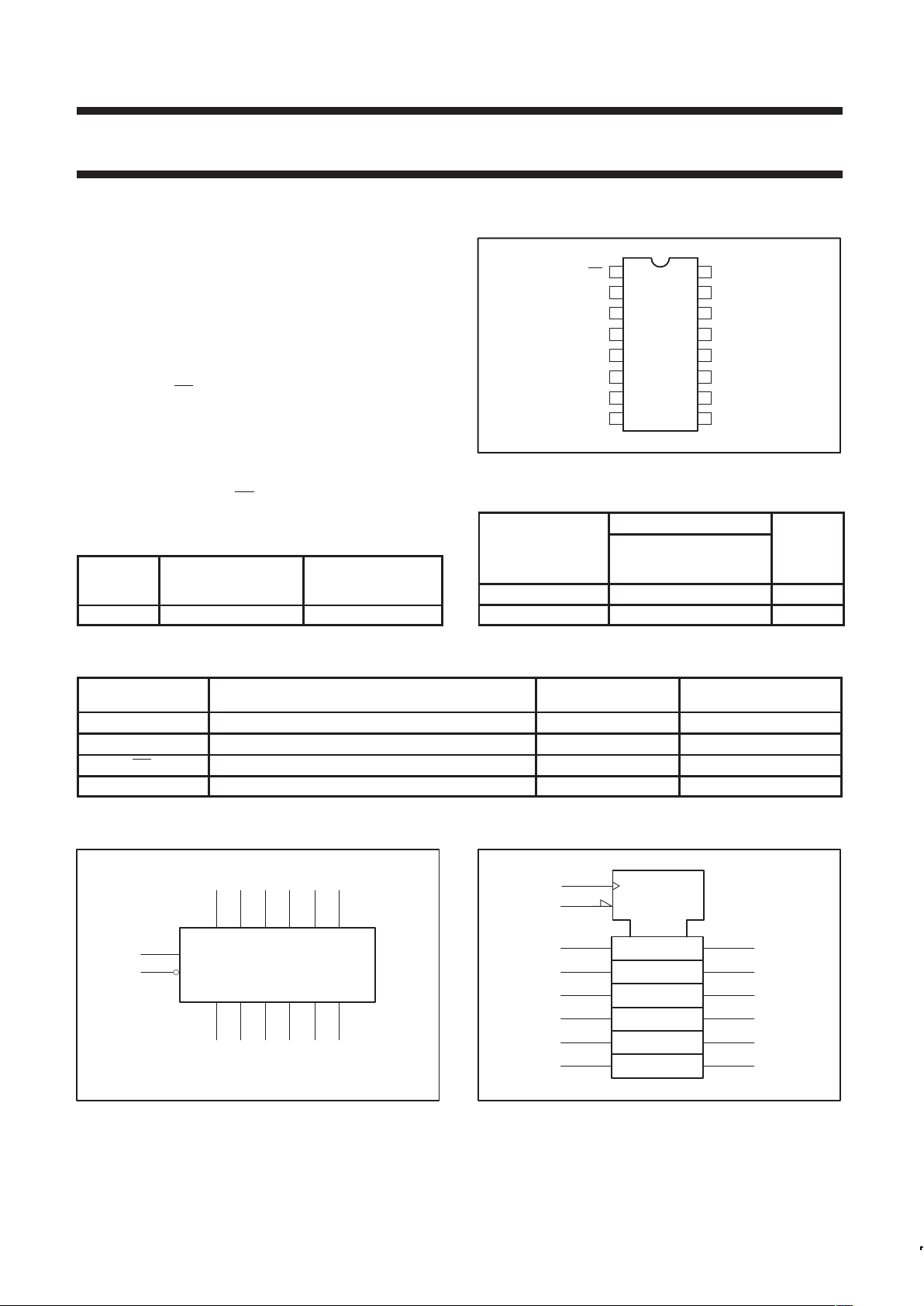
PIN CONFIGURATION
16
15
14
13
12
11
107
6
5
4
3
2
1
Q2
V
CC
Q4
D3
Q3
D4
Q5
D5
MR
Q0
D2
D0
D1
Q1
98GND CP
SF00188
ORDERING INFORMA TION
ORDER CODE
DESCRIPTION COMMERCIAL RANGE
V
CC
= 5V ±10%,
T
amb
= 0°C to +70°C
DRAWING
NUMBER
16-pin plastic DIP 74ALS174N SOT38-4
16-pin plastic SO 74ALS174D SOT109-1
INPUT AND OUTPUT LOADING AND FAN-OUT TABLE
PINS DESCRIPTION
74ALS (U.L.)
HIGH/LOW
LOAD VALUE
HIGH/LOW
D0 – D3 Data inputs 1.0/1.0 20µA/0.1mA
CP Clock Pulse input (active rising edge) 1.0/1.0 20µA/0.1mA
MR Master Reset input (active-Low) 1.0/1.0 20µA/0.1mA
Q0 – Q5 Data outputs 20/80 0.4mA/8mA
NOTE: One (1.0) ALS unit load is defined as: 20µA in the High state and 0.1mA in the Low state.
LOGIC SYMBOL
Q2 Q3 Q4 Q5
7101215
346
V
CC
= Pin 16
GND = Pin 8
SF00189
Q1
5Q02
9
1
CP
MR
D0 D1 D2 D3 D4 D5
11 13 14
IEC/IEEE SYMBOL
SF00190
3
1D
9
C1
1
R
4
6
11
13
14
2
5
7
10
12
15
Philips Semiconductors Product specification
74ALS174Hex D flip-flop
1991 Feb 08
3
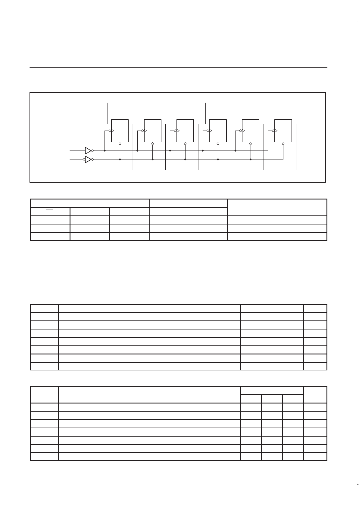
LOGIC DIAGRAM
SF00192
CP
D
R
D
MR
1
CP
9
V
CC
= Pin 16
GND = Pin 8
Q
D0
3
Q0
2
CP
D
R
D
Q
D1
4
Q1
5
CP
D
R
D
Q
D2
6
Q2
7
CP
D
R
D
Q
D3
11
Q3
10
CP
D
R
D
Q
D4
13
Q4
12
CP
D
R
D
Q
D5
14
Q5
15
FUNCTION TABLE
INPUTS OUTPUTS
OPERATING
MR CP D Q
n
MODE
L X X L Reset (clear)
H ↑ h H Load “1”
H ↑ I L Load “0”
NOTES:
H = High-voltage level
h = High state must be present one setup time before the Low-to-High clock transition
L = Low-voltage level
l = Low state must be present one setup time before the Low-to-High clock transition
X = Don’t care
↑ = Low-to-High clock transition
ABSOLUTE MAXIMUM RATINGS
(Operation beyond the limit set forth in this table may impair the useful life of the device.
Unless otherwise noted these limits are over the operating free air temperature range.)
SYMBOL
PARAMETER RATING UNIT
V
CC
Supply voltage –0.5 to +7.0 V
V
IN
Input voltage –0.5 to +7.0 V
I
IN
Input current –30 to +5 mA
V
OUT
Voltage applied to output in High output state –0.5 to V
CC
V
I
OUT
Current applied to output in Low output state 16 mA
T
amb
Operating free-air temperature range 0 to +70 °C
T
stg
Storage temperature range –65 to +150 °C
RECOMMENDED OPERATING CONDITIONS
LIMITS
SYMBOL
PARAMETER
MIN NOM MAX
UNIT
V
CC
Supply voltage 4.5 5.0 5.5 V
V
IH
High-level input voltage 2.0 V
V
IL
Low-level input voltage 0.8 V
I
IK
Input clamp current –18 mA
I
OH
High-level output current –0.4 mA
I
OL
Low-level output current 8 mA
T
amb
Operating free-air temperature range 0 +70 °C
 Loading...