

Page 1

Colour Television Chassis
MG5.1E
AA
Contents Page
1 MG99 Light path
2 Introduction
3 Overall blockdiagram
4 Power supply
5 Scan circuits
6 Small signal panel
7 CRT drive circuit
8 Interface panel
9 SIDE JACK panel
10 Audio signal part
11 Digital convergence circuit
2
8
9
11
24
29
69
72
74
75
80
©
Copyright reserved 1999 Philips Consumer Electronics B.V. Eindhoven, The
Netherlands. All rights reserved. No part of this publication may be reproduced,
stored in a retrieval system or transmitted, in any form or by any means, electronic,
mechanical, photocopying, or otherwise without the prior permission of Philips.
Published by LM 9972 Service PaCE Printed in the Netherlands Subject to modification 5 3122 785 10053
Page 2
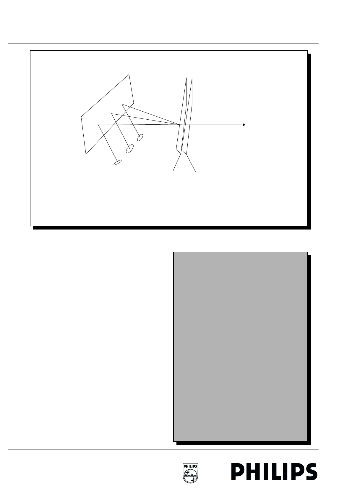
2 1. MG99 Light path MG5.1E
1. MG99 Light path
MIRROR
R+G+B
RED
GREEN
BLUE
FRESNAL
LENS
LENTICULAR
SCREEN
CL 96532100_078.eps
121199
The MG99 Projection TV uses three single color tubes, Red,
Green, and Blue. (Figure 1-1) The output of each tube is
projected onto a mirror where it is then reflected onto a viewing
screen. The Tubes are converged so the light from each tube
strikes the same spot on the Fresnel Lens. The Fresnel Lens
equalizes and concentrates the light to provide equal light
uniformity across the screen. The Mirror is a first surface mirror
type which has the reflective coating on the outside of the
mirror. To prevent scratching of this surface, always use a soft
cotton cloth to clean it.
Figure 1-1
Personal notes
Page 3
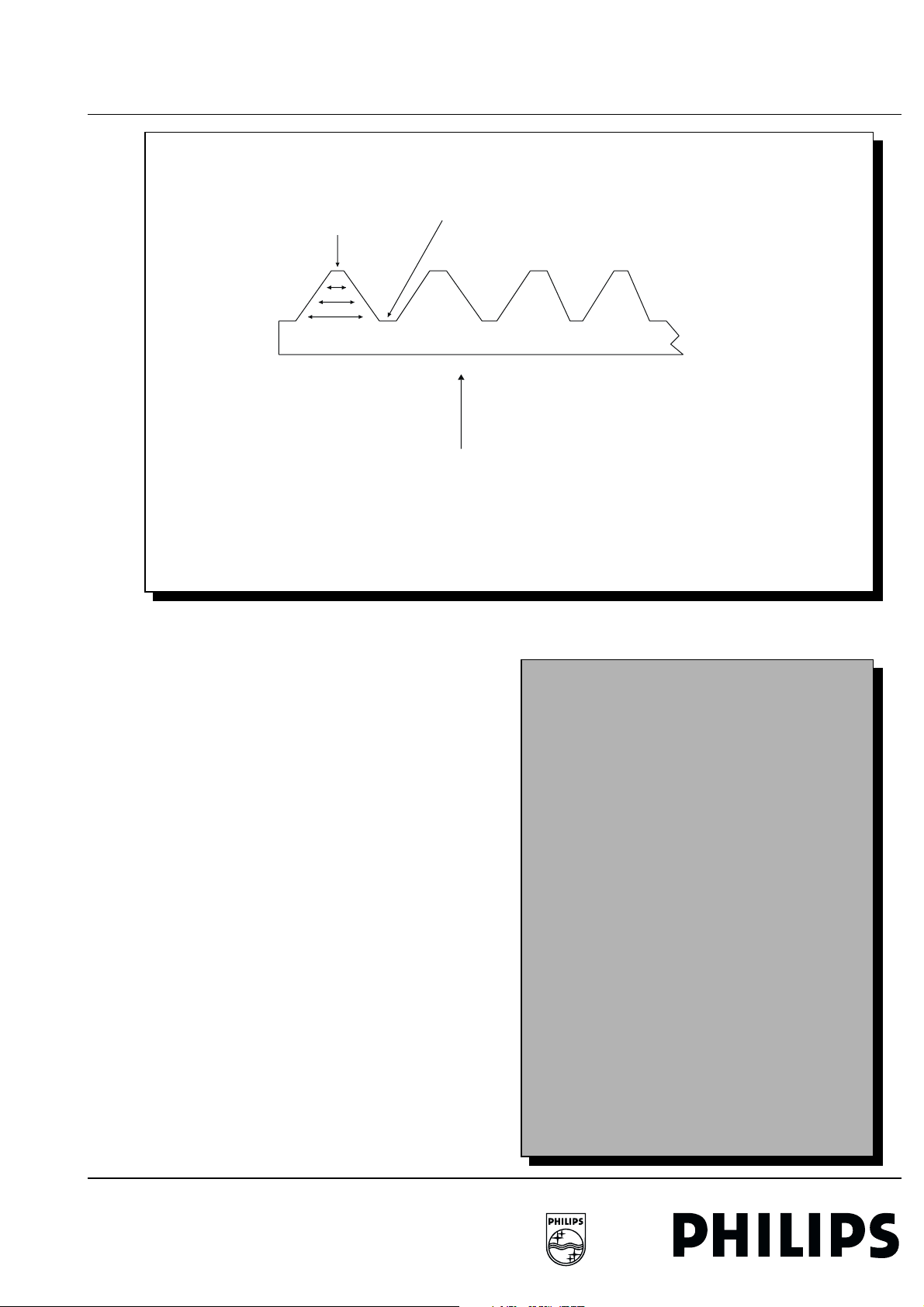
MG5.1E 1. MG99 Light path 3
OUTPUT
BLACK STRIPING
LIGHT
Figure 1-2
CL 96532100_079.eps
111199
The Lenticular Lens Screen calumniates the light from the
Fresnel Lens. (Figure 1-2) The Lenticular Lens increases
contrast by reducing the ambient light by the use of Black
Striping. The Prismatic formation of the screen allows for nearly
3X light output as compared to a flat screen. Caution should be
used when working with the screen. Damage can easily occur
in the form of scratching, or by using certain chemical screen
cleaners which can strip the black striping from the screen. To
clean the screen, use one drop of dish washing detergent in a
small bowl of water. (approximately 2 liters) Wipe the screen
with a soft cotton cloth in the direction of the stripes.
Personal notes
Page 4

4 1. MG99 Light path MG5.1E
C ELEMENT LENS
CRT
LIQUID COOLANTOUTPUT LENS
The Three CRT's are driven by 30KV of high voltage and 15KV
of focus voltage. (Figure 1-3) The Tube produces a highly
concentrated light output of color. A liquid coolant of Glycol is
used to transfer heat from the face of the tube to the
surrounding mechanical assembly. The
C-element lens seals the Coupling fluid within the coupler. The
C-element lens and Coupling fluid are part of the light path and
contribute to the properties of the optical system.
Figure 1-3
Personal notes
CL 96532100_080.eps
111199
Page 5

MG5.1E 1. MG99 Light path 5
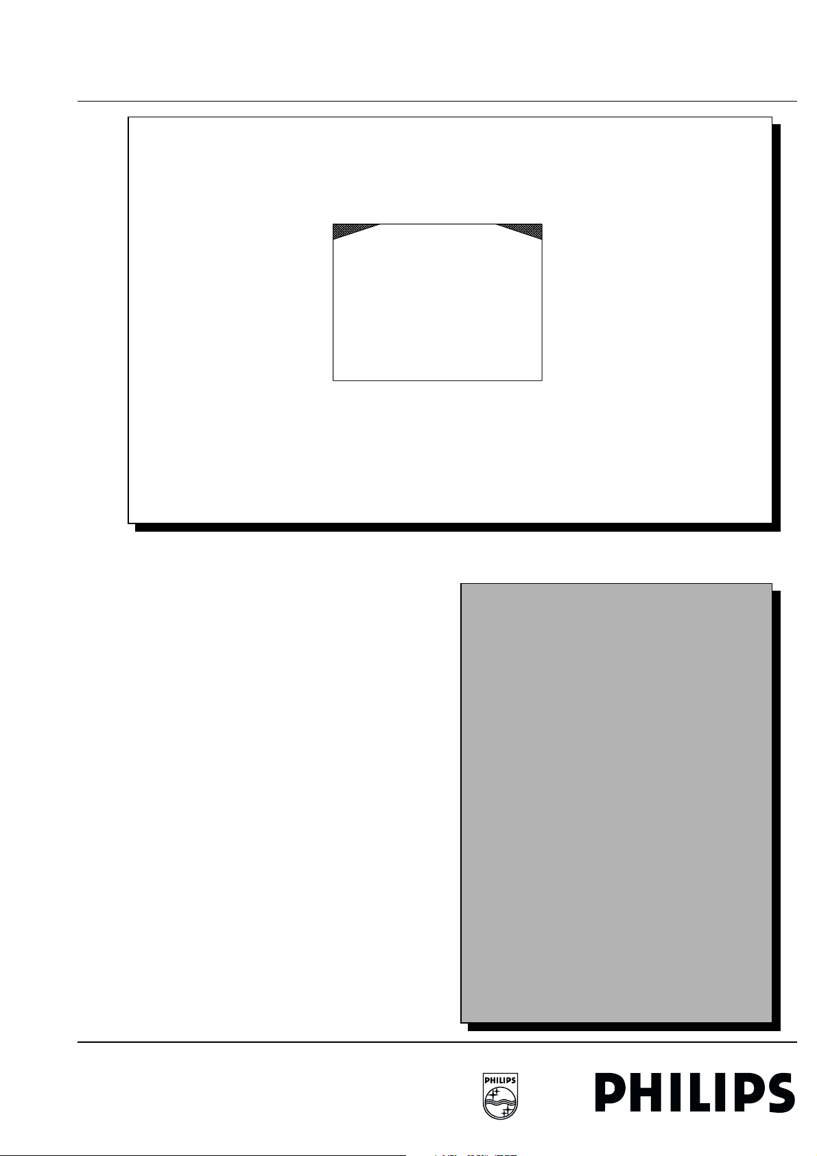
1.1 MG99 LIGHT PATH PROBLEMS
1.1 MG99 LIGHT PATH PROBLEMS
Look at the edges of the screen. They may be bowed inward.
PROBLEM - BOTTOM CORNERS DARK
PROBLEM - BOTTOM CORNERS COLORED
There is no problem with the set. The viewing angle is too high.
Figure 1-4
Personal notes
CL 96532100_107.eps
021299
Page 6

6 1. MG99 Light path MG5.1E
1.1 MG99 LIGHT PATH PROBLEMS
Fresnel may be reversed. Carefully remove the fresnel and
point the grooves toward the viewer.
PROBLEM - BRIGTH AND DARK LINES ON A WHITE FIELD
Figure 1-5
CL 96532100_109.eps
151199
Personal notes
Page 7
MG5.1E 1. MG99 Light path 7
1.1 MG99 LIGHT PATH PROBLEMS
The Fresnel offset is pointing down. The center of the Fresnel
should be toward the top of the screen.
PROBLEM- UPPER CORNERS OF THE SCREEN DARK
Figure 1-6
CL 96532100_110.eps
151199
Personal notes
Page 8

8 2. Introduction MG5.1E
2. Introduction
The 1999 MG99 PTV chassis is designed for the European
market. It is available in a 46 inch (117 cm) and a 55 inch (140
cm) 16 by 9 aspect ratio screen sizes. Selected Video can be
displayed in either a 4 by 3, 14 by 9, or 16 by 9 aspect ratios.
The set has a viewing angle of 160 degrees.
The MG99 PTV is capable of receiving signal from PAL B/G,
PAL B/G 6OHz, PAL B/H, PAL D/K, PAL 1, PAL M, PAL N, PAL
plus, SECAM B/G, SECAM D/K, SECAM L, AND SECAM Li TV
systems. There are four composite video inputs which include
three SCART connectors, and a Side Jack panel. The systems
that can be applied to these inputs are NTSC 3.58, NTSC 4.43,
NTSC Play Back, PAL 4.43, PAL, B/G Play Back, SECAM, and
SECAM Play Back.
The set is equipped with a Frame and Line doubler to produce
a horizontal resolution greater than 800 lines. The picture
display is driven by three seven inch Red, Green, and Blue
tubes.
The Sound system is driven by a 2 times 20 watt power
amplifier. A switch in the rear of the set allows the sets internal
speakers to be driven by an external amplifier.
The following sets will be sold in Europe:
46PP9501/05U.K. and Ireland
55PP9501/05U.K. and Ireland
46PP9501/12Western Europe
55PP9501/12Western Europe
46PP9501/58Eastern Europe
55PP9501/58Eastern Europe
These units will be distributed from Philips Bundling Center in
Bruges, Belgium.
Personal notes
Page 9

9 3. Overall blockdiagram MG5.1E
3. Overall blockdiagram
Y_CVBS
SIDE JACK
PANEL
MG99 SMALL
SIGNAL PANEL
C
L
R
Y
R
G
B
CRT
DRIVE
CIRCUIT
DELAY
SVM
MODULE
BLUE
CRT
R
G
B
GREEN
CRT
RED
CRT
AC
SWITCH
PANEL
LINE SYNC
FRAME SYNC
POWER
SUPPLY
CONV R, G, B, FB
LEFT AUDIO
RIGHT AUDIO
+5V STBY
+15V STBY
+130V
+38V
-38V
+33V
+15V
-15V
-7V7
+8V6
+5V2
INTENSITY
CONTROL
INTERFACE PANEL
AUDIO
AMPLIFIER
LINE
DRIVE
FRAME
DRIVE
HV
CIRCUIT
HV/SCAN
PANEL
SPEAKER
SWITCH
CONV R, G, B, FB
CONVERGENCE
PANEL
LINE SYNC
FRAME SYNC
FOCUS/G2
BLOCK
CONV
YOKES
FOCUS
G2
CL 96532100_081.eps
191199
Figure 3-1
Page 10

10 3. Overall blockdiagram MG5.1E
There are eleven PC boards in the MG99 chassis. (Figure 3-1)
They are the Small Signal panel, Side Jack panel, Power
Supply panel, Interface panel, SVM module, Blue CRT panel,
Green CRT panel, Red CRT panel, High Voltage Scan panel,
and Convergence panel.
Whenever AC power is applied to the set and the Mains switch
is turned On, the Power Supply panel produces a 5 and a 15
volt standby supplies. When the set is turned On by the channel
up button on the Front Keyboard or the Remote Control, the
130 volt, 38 volt, -38 volt, 33 volt, 15 volt, -15 volt, -7.7 volt, 8.6
volt, and 5.2 volt supplies are switched On.
Frame and Line drive from the Small Signal panel is routed
through the Interface Panel to the Frame Drive and Line Drive
circuits on the High voltage Scan panel. The High Voltage scan
panel produces the High Voltage and Sync to the Convergence
panel. Focus voltage from the High Voltage circuit is fed to a
Focus/G2 block which provides Focus and G2 voltage to the
three CRT'S. During the Convergence adjustment mode, Red,
Green, Blue, and Fast Blanking from the Convergence Panel is
fed to the Small Signal panel to generate the adjustment grid.
The Small Signal panel selects video from the Antenna input,
one of the three Scart connectors, or the Side Jack panel. The
Small Signal panel outputs Red, Green, and Blue drive to the
CRT drive circuit located on the Interface Panel. The CRT drive
circuit then provides drive for the three CRT panels.
Personal notes
Left and Right channel audio from the Small Signal panel is
routed through the Interface Panel to the Audio Amplifier panel.
The Audio Amplifier panel has its own separate Switch Mode
power supply. The output of the Audio Amplifier is then fed to
the Speaker Switch panel which selects between the Audio
Amplifier or External Audio from a separate amplifier.
Luminance or Y from the Small Signal panel is fed to a Delay
circuit on the Interface panel before being applied to the SVM
panel. The Scan Velocity Module speeds up the beam during
light to dark transitions in the picture to provide a sharper
image.
Page 11

11 4. Power supply MG5.1E
4. Power supply
AC
INPUT
CIRCUIT
AC
SWITCH
PANEL
POWER
FACTOR
CORRECTION
CIRCUIT
STBY
POWER
SUPPLY
+5V STBY
+15V STBY
ON/OFF
AC power is applied to the set on the Power Supply panel.
(Figure 4-1) It is then fed to the Mains switch on the AC switch
panel located on the front of the set. It is then fed back to the
Power Supply panel and to the Power Factor Correction circuit.
If the AC mains is 240 volts, the output of the Power Factor
correction circuit is approximately 329 volts DC in standby and
350 volts DC when the set is turned On. The Power Factor
correction circuit is turned Off during standby. This is a "HOT"
chassis. When troubleshooting this or any power supply,
always use an isolation transformer.
The Standby Power supply produces a 5 and a 15 volt supplies.
It also provides operating voltage for the Power Factor
Correction and the Audio Amplifier power supply. The Power
Factor correction circuit is turned Off when the set is in the
Standby mode.
The Main Switch Mode Power supply produces a 130 volt, a 33
volt, a 35 volt, a -35 volt, a 15 volt, and a
-15 volt supply. The Main SMPS and the Power Factor
Correction Circuit is switched On by a Low from the Small
Signal panel.
Figure 4-1
MAIN
SMPS
POWER
SUPPLY
+15V
+15V
-15V
5V2
REG
8V6
REG
-7V7
REG
Personal notes
+130V
+33V
+35V
-35V
+15V
-15V
+5V2
+8V6
-7V7
CL 96532100_082.eps
121199
Page 12
MG5.1E 4. Power supply 12
TO AC SW BD
1221
1000
5A
2000
680n
3011
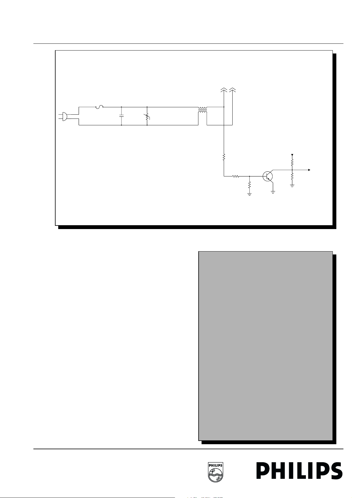
The applied AC voltage is fed to a 5 amp fuse and then to the
Mains switch on the AC switch panel. (Figure 4-2) The AC
voltage is fed to transistor 7000 and then to the Small Signal
panel for clock synchronization.
Figure 4-2
4
5001
1
3004
3.3M
3005
3.3M
3006
470K
Personal notes
7000
3007
6.8K
+5VSTBY
3008
10K
50_60HZ
CL 96532100_083.eps
121199
The Standby Supply produces the 5 volt and 15 volt standby
supplies. (Figure 4-3) The output of the Power Factor correction
circuit PFCOUT is applied to Pin 5 of 7211 through Pins 2 and
4 of the switching transformer 5202. When the supply voltage
is first applied, voltage through the internal startup resistor Rs
is applied to capacitor 2283 via Pin 4. When the capacitor
charges to 5.7 volts, the internal oscillator switches On driving
the internal FET switch. When the voltage across capacitor
2283 drops below 4.7 volts, the IC turns Off. This cycle repeats
until the 5 volt standby supply turns Shunt Regulator 6205 On.
The supply voltage for the IC is then supplied to Pin 4 through
7213. Operating voltage to Pin 5 of 7213, the Audio Amplifier
power supply, and the Power Factor correction circuit is
supplied by Pin 5 of 5202. During normal operation, the 5 volt
standby source is monitored by the Shunt Regulator 6205. If
the 5 volt supply should increase, the Shut Regulator will cause
more current to flow through the LED inside the opto-isolator
7213. This will reduce the resistance of the transistor inside
7213. As a result, more current will flow through the Sensing
resistor inside 7211, which will reduce the On time of the FET
inside the IC. This will reduce the output voltage to the correct
level. This supply operates at approximately 100 KHz.
Page 13

MG5.1E 4. Power supply 13
RESET
+5VSTBY
SOURCE
2282
1uF
5234
3245
2210
7209
RESET
3222
+15VSTBY
2270
6204
1098
2
6200
6207
22uF
3240
1K5
100uF
4
6236
1K
39K
6231
3247
180
3246
2K4
2213
1000uF
+5VSTBY
2208
100
2226
3223
22n
3239
2K4
3244
33K
47
1
6205
SHUT
REGULATOR
2
7213
4
5
3287
470
5
CONTROL
5214
+5VSTBY
3215
5233
5211
7204
3241
1K
PFC
1
6K8
7208
GND_C
6201
8.2V
2209
100uF
3230
1K5
2211
.1
3216
6235
2269
100
7
5202
1
5
GND_C
2228
100
10
3213
10K
5
GND_C
4
7206
2
7205
+5VSTBY
3212
10K
7214
3289
3214
10K
ON_OFF
100K
2284
3288
10n
10K
PFCOUT
Figure 4-3
2206
GND_C
220uF
S
R
7211
INTERNAL
4
SUPPLY
PWM
-
5.7V
4.7V
S
R
5.7V
GND_C
1,2,3,7,8
2283
CL 96532100_084.eps
011299
GND_C
47uF
Page 14

14 4. Power supply MG5.1E
To troubleshoot the Standby Supply, first check the supply
voltage on Pin 5 of 7211. If there is no secondary voltage and
7211 is working correctly, startup pulses should be seen at Pin
5 of the IC. If the IC is pulsing and there is no secondary
voltage, there is a problem with the outputs of 5202 or with the
feedback circuit. If 7211 is not pulsing, either the IC or capacitor
2283 is defective.
When the set is turned On, transistor 7214 will turn Off turning
7205 On. This will turn the Optoisolator 7206 On turning
transistor 7204 On, switching the operating voltage to the
Power Factor Correction circuit. It also switches the operating
voltage to the power supply on the Audio Amplifier panel on the
line labeled "CONTROL".
Personal notes
Page 15

MG5.1E 4. Power supply 15
4.1 European power factor correction circuit
4.1 European power factor correction circuit
AC IN
AC CURRENT
CAPACITOR
CHARGE
VOLTAGE
BRIDGE
AB
The input to most switching power supplies consists of a bridge
rectifier and a large electrolytic capacitor. (Figure 4-4) When
AC power is applied, the Capacitor will charge to approximately
1.4 times the RMS value of the applied AC voltage. This type of
supply does not draw current from the AC power source
through out the entire AC cycle. When the capacitor charge falls
to point "A", the instantaneous value of the AC voltage exceeds
the charge of the capacitor. The bridge diodes are then forward
biased, causing current to flow from the AC source. Current will
continue to flow from the AC line until the AC sinusoidal voltage
reaches its peak at Point "B". At this point, the charge on the
capacitor will exceed the AC line voltage reversing the bridge
diodes. This results in an AC current waveform that is narrow
and distorted compared to the AC voltage waveform. Non
sinusoidal waveforms have a high harmonic content, with
excessive peaks which results in a low power factor of 0.5 to
0.6. Power Factor is a ratio of real power divided by apparent
power. Excessive harmonics and peak currents reduce the
efficiency of the power distribution system.
The MG5.1 Projection TV without Power Factor correction has
a high harmonic content of 85 percent, creating a Power Factor
of 0.5. Current spikes of 7 amps will also be created in the AC
supply. With the Power Factor correction circuit, the peak
current is limited to 1.58 amps, with the harmonic content being
reduced to 4.5 percent. The Power Factor is increased to 0.99.
The ideal Power Factor is one, which occurs when the current
is sinusoidal and in phase with the voltage. The European
standard IEC1000 limits the current harmonic content of
equipment supplied by the AC Mains.
Figure 4-4
CAP
CL 96532100_085.eps
LOAD
121199
Personal notes
Page 16
16 4. Power supply MG5.1E
4.1 European power factor correction circuit
AC INPUT
BRIDGE
CURRENT SENSE
REGULATOR
DRIVE
7102
The MG5.1 Power Factor correction circuit uses a Boost
regulator to smooth out the current draw from the AC line
improving the Power Factor to 0.99, which is accomplished by
drawing current from the AC source throughout the entire AC
cycle making the current waveform sinusoidal. (figure 4-5) Input
to the module is connected to the AC Mains. The output
supplies are approximately 350 volts DC to the Main and
Standby Switched mode Power Supply circuit. The Boost
Regulator circuit produces a higher output voltage than the
input voltage. The regulator drive circuit compares 6103's
output voltage, the input voltage from the bridge, and the
voltage across the current sensing resistors to control the On
time of 7104. This will maintain the output voltage at 350 volts
DC and limit the input current to acceptable levels. When 7104
is On, current flow through 5109 stores energy in the choke.
When 7104 turns Off, 5109 reverses polarity and charges 2110.
Using this type of regulation, current is drawn from the AC
source throughout the entire cycle, keeping the current
waveform sinusoidal. When the AC cycle is at its low point,
7104 is on for a longer period of time. When the AC voltage is
at its peak, 7104 is on for a shorter time to store the same
amount of energy in 5109 to maintain the output voltage at 350
volts.
Figure 4-5
5109
5
3
6103
7104
2110
350V DC OUT
CL 96532100_086.eps
121199
If the Boost regulator circuit should become inoperative, due to
a loss of regulator drive, operating voltage is still applied to the
set. The supply voltage to the switching supplies will drop from
350 volt to approximately 329 volts depending on the Mains
voltage. Since the customer would not detect a failure, the
operation of this circuit should be checked after any repair of
the set.
Page 17

MG5.1E 4. Power supply 17
4.2 Full power factor correction circuit
350V DC OUT
PFCOUT
(329V)
GND_C
2105
3105
470p
5106
5103
6R8
6103
5105
35
5109
GND_B
2107
1n
3126
3M3
GND_B GND_B
2118
47K
1uF
3125
GND_B
1K
3119
GND_B
2120
7104
3117
220p
10K
GND_B
GND_B
PFC
2113
3115
100uF
47
GND_B
6104
3114
5108
19V
(25V)
47
20
15
LATCH
LOGIC
1.28
-
+
R
OUTPUT
Q
S
VCC
19
16
2110
470uF
5107
13
15
OVP
V REF
5.11 V
4.3V
3
3134
470K
3108
3M3
3110
39K
3109
47K
11
5006
3010
5003
2R2
1222-1
5005
3120
5K6
0.23V
IPK
5.11V
2
5.45V
5
9
8
5.45V5.11V
13
14
3127
3118
390
2116
2n2
18K
GND_B
3128
1K8
3123
1K8
2115
.33
3124
330K
CL 96532100_087.eps
191199
+
-
2114
R490
1M
C485
C486
R493
1n5
3121
33K
3111
1M
.22
.22
INST LINE VOLTAGE
33K
STARTUP VOLTAGE
FOR FULL
POWER SECTION
6000
0.36V MAX
3133
0R1
3132
0R1
R491
5004
5007
3131
3130
FROM AC
SW BOARD
1222-4
0R1
0R1
GND_B
GND_HA
330K
OSCILLATOR
17 18
7102
4
7
1.5-5.5V
GILBERTS
6
5.11V
+
MULTIPLIER
-
COMPARATOR
CURRENT
AMPLIFIER
-
+
Figure 4-6
Page 18

18 4. Power supply MG5.1E
4.2 Full power factor correction circuit
An explanation of the full Power Factor Correction circuit is now
given. (Figure 4-6) The Power Factor Correction circuit is a
fixed-frequency Pulse-Width modulated boost regulator power
supply. Operating frequency is approximately 60 kilohertz. Due
to the low power consumption of the set during the standby
mode, the Power Factor Correction circuit is turned Off. The
operating voltage, PFC, on Pin 19 of 7102 is turned Off. When
the set is turned On, the operating voltage is switched to Pin 19
of 7102. Once the circuit is in operation, a 5.11 volt internal
reference voltage on Pin 11 is applied to Pin 6 of the IC. Output
of the bridge rectifier is fed to the IC on Pins 4 and 7. Feedback
from the output circuit is fed to Pin 14 where it is multiplied with
the Bridge output. Inputs to the Gilberts Multiplier produce an
error signal that is fed to the current amplifier. The Gilberts
Multiplier multiplies the bridge output voltage with the output
voltage on D438. The 5.11 volt reference is used to provide a
clamping reference for the other inputs. Input current is
sampled by resistors 3130, 3131, 3132, and 3133. This sample
is added to the error signal from the Multiplier going into Pin 8.
The error signal is amplified and then compared to the oscillator
ramp to determine the reset point for the latch. When the
oscillator goes low, the latch is set making output "Q" High. With
the other inputs to the AND gate High, Pin 20 then goes High,
turning 7104 On. By comparing the input and output voltage,
the On time of 7104 is increased when the AC voltage is at its
low point to maintain the 350 volt DC output. When the AC input
voltage is at its peak, 7104 is On for a shorter period.
Personal notes
The IPK circuit connected to Pin 2 is an overcurrent protection
circuit which resets the latch if there is excessive current
through the return resistors. This will reduce the On time of
7104. In a like manner, the OVP, Over Voltage Protection,
circuit will reset the latch removing drive to Pin 20 is the output
voltage exceeds 392 volts.
To check the operation of this circuit when the set is operating
correctly, check the PFCOUT voltage. This voltage should be
approximately 350 volts. If the output voltage is approximately
329 volts, this circuit is not working. Check the operating
voltage on Pin 19 of 7102. Then check the output drive on Pin
20 and at the gate of 7104. There are three grounds on the Hot
side of the supply. Ground HA is connected directly to the
bridge 6000. Ground "B" is the ground for the Power Factor
Correction circuit. If the current sensing resistors 3130 through
3133 should open, this would remove the ground for all the
switching supplies and make the set inoperative. Ground "C" is
the ground for the switching supplies. When ground "B" passes
through the choke 5106, it becomes ground "C".
Startup up voltage for the Full Power supply is taken from the
neutral side of the AC mains.
Page 19

MG5.1E 4. Power supply 19
4.3 Full power supply
+15V
2326
3331
3330
22K
22K
2312
+33V
470P
5305
5304
+130V
14
4
PFOUT
2314
6305
2350
2313
22uF
470uF
470P
6
3446
3346
12
470R
3345
6315
10
470R
8
+35V
2318
100n
2317
1000u
5307
2316
1000u
2315
5306 6306
1516171819
3307
33R
2
470p
7301
6304
5302
100n
-15V
2332
-35V
5314
100n
1000u
1000uF
2319
1V
+
B
FLIP
470p
3308
6302
3310
2307
-
FLOP
3309
1302
0R47
0R1
330R
4A
6309 5313
202122
10
11
GND_C
GND_C
6303
2311
1N
2308
R
2331
2330
2319
GND_C
2322
2321
2321
63075308
3305
10K
GND_C
3306
10R
3
4
7
A
Q
S
100n
100n
470u
2327
470u
3329
330R
2328
3319
12
3328
1u
100R
3326
4K7
1
7303
VCC
5
6301
2302
3316
1K
GND_C
15K
GND_C
3318
150K
VCC
GND_C
GND_C
2324
14
-
5312
2m2
2323
470p
3315
15K
2.5V
+
C
5312
2325
100n
1301
4A
5310
6308
470p
3447
2.7K
3317
15K
5
13
FB
7302
3324
150K
3323
2K7
+130V
2334
3325
10K
3327
100R
2303
STARTUP
3300
100uF
22K
3461
27K
GND_C
2333
24
7303
+5VSTBY
3322
3344
7309
3304
1K
7300
1305
+5VSTBY
470R
130V
10K
ADJ
ON_OFF
3343
3303
100K
2349
10K
6313
3321
SOFT
UNDER
2346
100N
VCC
START
VOLTAGE
LOCKOUT
9.4/14.5
18V
1
8K2
6
17V
3320
OVERVOLTAGE
8K2
VCC
GND-C
DEMAG
VCC
8
OSCILLATOR STANDBY
REFERENCE
SECTION
9
FROM
STBY
SYNC
2442
1N
10
11
2443
1uF
15
16
3313
10K
CL 96532100_088.eps
011299
Figure 4-7
Page 20

20 4. Power supply MG5.1E
4.3 Full power supply
When the set is turned On, the Main Switch Mode power supply
is turned On. (Figure 4-7) This supply produces the +130 volt,
+33 volt, +35 volt, -35 volt, -15 volt, and +15 volt supplies.
When the On/Off line goes Low, transistor 7309 is turned Off,
turning transistor 7300 On. This switches relay 1305 On.
Startup voltage from the neutral side of the AC mains will
charge capacitor 2303 to 14.5 volts which will overcome the
undervoltage lockout of IC 7302. After the Soft Start capacitor
2443 charges, the oscillator inside the IC will turn On. Each
cycle of the oscillator will set the flip-flop which will cause Pin 3
to go High. This will turn the FET switch 7301 On. Voltage is
applied to the Drain of 7301 through Pins 4 and 8 of 5300 from
the Power Factor Correction circuit. Current through sensing
resistors 3308 and 3309 will develop a voltage which is applied
to comparator "B" connected to Pin 7. When the voltage on Pin
7 reaches the reference voltage on the inverting input, the FlipFlop will be reset. The voltage on the inverting side of
comparator "B" is limited to 1 volt. Therefore, the ramp voltage
on Pin 7 will not exceed 1 volt. The circuit will continue to
operate until the charge on capacitor 2303 falls below 9.4 volts
shutting the IC Off. Each time 7301 is turned On, energy is
stored in transformer 5300. Voltage from the Hot secondary on
Pin 10 is rectified by 6301. When the output of this circuit has
sufficient energy to maintain 2303 above 9.4 volts, the IC then
operates in steady state.
Personal notes
When IC 7302 develops a normal steady state operation, the
130 volt supply is sampled by resistors 3324, 3323, and 3322.
This sample voltage is then sent to Shunt regulator 7303 which
drives the feedback optoisolator 7303. The feedback voltage on
Pin 14 is then compared with an internal 2.5 volt reference by
comparator "C". Comparator "C" then sets the reference
voltage on the inverting side of comparator "B" to control the On
time of the drive at Pin 3. If the voltage on Pin 14 increases due
to the 130 volt supply increasing, the On time of the pulse on
Pin 3 will be reduced. If the 130 volt supply decreases, the
voltage on Pln 14 would decrease, causing the On time of the
pulse on Pin 3 to increase. This is used to keep the 130 volt
supply at the correct voltage. Variable resistor 3322 is used to
adjust the 130 volt supply to the correct level.
The overvoltage protection circuit of the IC will shut the IC down
if the VCC level on Pin 1 exceeds 17 volts.
To troubleshoot this circuit, first check the On/Off line from the
Small Signal Panel to ensure that it is going Low. Then check
for the presence of startup voltage on Pin 1 of the regulator IC
7302. If the IC is working correctly, this voltage will be changing
from 9.4 to 14.5 volts. If the startup voltage is not present, check
the startup resistor 3300 and the bridge rectifier. If the voltage
on Pin 1 is changing, check the drive signal on Pin3. Then
check for signal on the gate and drain of 7301. An excessive
load on the secondary, a short on the 130 volt line for example,
would cause the supply to pulse with little or no voltage on the
secondary.
Page 21
MG5.1E 4. Power supply 21
191199
TO SCAN
HIGH VOLTAGE
TO
AUDIO
AMPLIFIER
TO
CONVERGENCE
PANEL
PANEL
CL 96532100_052.eps
TO
INTERFACE
PANEL
11
50/60 HZ
10
STBY RTN
9
+5V STBY
-7V7
8
SSGND
7
6
SS GND
5
5V
+8V6
4
3
+15V
2
130V RTN
+130V
1
1202
160V DCNC160V RTN
1
CONTROL
+15V
-35V
-35V
RTN
RTN
+35V
+35V
-15V
15V RTN
+15V
+15V
+15V RTN
+5V STBY
STBY RTN
ON/OFF
NC
2
3
4
1203127612121205
1
234
1
56789
2
1210
4
3
POWER
SUPPLY
567
PANEL
8
9
10
1222
5
4
6
1221
1
2
3
+130V
4
+130V
+130V RTN
213
1220
+130V RTN
SS GND
SS GND
+5V2
+5V2
TO
MG99
+8V6
5V STBY
SMALL
SIGNAL
PANEL
+33V
+15V
ON/OFF
Figure 4-8
AC SW BOARD
Page 22

22 4. Power supply MG5.1E
4.3 Full power supply
The Power Factor Correction, Standby, and Full Power circuits
are all located on the Power Supply panel. (Figure 4-8) The
Standby supply feeds the 5 volt standby supply to the Small
Signal panel via Pin 5 of connector 121 0. The Standby voltage
is present whenever power is applied to the set and the Mains
switch is On. The On/Off Command from the Small Signal panel
is fed to the Power Supply on Pin 8 of connector 121 0. This Pin
will measure 5 volts when the set is in the standby mode and 0
volts when the set is turned On. The +33, +15, +8.6, and +5.2
volt supplies to the Small Signal panel are developed after the
set is turned On.
The +130, +15, +8.6, -7.7, and 5 volt standby voltages are fed
to the Interface panel on connector 1202. The 50/60 Hz signal
is a sync signal from the AC power mains which is used to
provide sync to the clock circuit on the Small Signal panel.
350 volts from the Power Factor Correction circuit is fed to the
Audio Amplifier on connector 1203. The Control line on Pin 4 of
1203 provides the operating voltage for the switching power
supply on the Audio Amplifier panel. This Control voltage is
switched Off when the set is in the Standby mode.
Connector 1276 routes power to the Convergence panel while
connectors 1212 and 1211 feeds power to the Scan High
Voltage panel.
Personal notes
Page 23

MG5.1E 4. Power supply 23
4.3 Full power supply
AC INPUT
BRIDGE
CURRENT SENSE
REGULATOR
DRIVE
7102
The +15 volt source is fed to transistor 7308. (Figure 4-9) This
is a Buck Switch regulator circuit which produces the 5.2 volt
source. Transistor 7308 is turned On and Off by the Switching
regulator IC 7307. To maintain the 5.2 volt source at the correct
voltage, the output is sampled and fed to Pin 5 of the IC. The
voltage on Pin 5 is then compared with an internal reference.
This drives the Pulse Width Modulator which controls the On
time of 7308.
Figure 4-9
5109
5
3
6103
7104
Personal notes
2110
350V DC OUT
CL 96532100_086.eps
121199
The -15 volt source is fed to linear regulator 7305 to produce
the -7.7 volt source. The +15 volt source is also fed to the 8.6
volt regulator 7306 to develop the 8.6 volt source.
Page 24

24 5. SCAN CIRCUITS MG5.1E
5. SCAN CI RCUITS 5.1Lin e Drive
RED
YOK E
GREEN
YOK E
BLUE
5801
10
2825
470p
9
FIL
3818
1R
8
3865
+240V
+13V
6802
12
0R47
2815
+130V
7
2827
2824
13
680p
1000u
3819
3815
3828
68K
2816
68K
1R
470p
14
6
0R27
6801
-13V
6803
5
2814
3825
2826
1000u
2850
+130V
68u
68K
470p
3867
3
3823
1R
68K
15
+28V
A
6850
16
1
2851
100u
2899
4n7
7802
2822
2818
3821
2817
430n
820p
470R
3n3
6806
2811
330p
3814
33R
2834
2819
5805
430n
5804
27n
6808
5803
2805
3681
100n
3452
2K2
YOK E
4R7
3805
+15V
100R
2573
3590
3453
2n2
100K
4R7
2u2
2452
7552
3457
2K2
3454
7553
4R7
7551
3591
3571
3455
3456
2K2
2K2
4R7
100R
3458
2K2
2820
A
4u7
3834
1R
3835
3K3
2836
6830
2837
LV
3806
2838
3837
1K
1n
12K
1
4
5802
6
8
1n
3839
330K
7830
2839
10n
10u
3812
100K
+130V
2809
100n
3811
3810
2810
2898
2K2
2K2
330u
220U
2806
1n
2807
4
1
3808
100n
3813
3
2
2K2
3807
1R
5800
330R
7803
3829
7801
3809
3830
15R
1509-1
330R
470R
+15V
HDRV
LINE
DRIVE
Figure 5-1
+28V
2801
100n
3803
100R
3840
2800
1M
1u
E_W
7800
3802
3866
3801
68K
18K
27K
1507-4
H_PUL
3800
3890
100R
1K5
1511-1
HFB
3817
470R
HPUL
+15V
1509-7
FBSO
3836
270R
+28V
3831
3832
3K3
7804
3833
100R
HPUL_BLNK
CL 96532100_089.eps
68K
2804
10u
121199
Page 25

MG5.1E 5. SCAN CIRCUITS 25
5.1 Line Drive
Line Drive from the Small Signal panel is fed to connector 1509
Pin 1 and then to buffer transistor 7803. (Figure 5-1) Transistor
7803 then drives the Line driver transistor 7801. Line drive is
then fed to the Line output transistor 7802. Transistor 7802
drives the three Line Yokes and the Scan transformer 5801.
The Scan transformer produces a 240 volt supply for the CRT
drive circuits, a Filament drive for the CRT'S, a plus and minus
13 volt supply for the Frame drive circuit. It also produces a 28
volt supply for the beam limiter circuit in the High Voltage circuit.
The output of the Line Output transistor 7802 is also fed to
buffer transistors 7800 and 7804 to produce a Line Sync pulse
(HPUL) and Line feedback pulses to the Small Signal panel (HPUL and HFB). The output of transistor 7804 also produces a
Line Blanking pulse (HPUL-BLNK).
Drive for geometry correction from the Small Signal panel on
the E-W line drives transistors 7553, 7551, and 7552. This
circuit drives the return side of the Line Yokes to provide
Horizontal corrections to the geometry. Geometry correction
drive, E-W, is also fed to transistor 7830 which produces drive
for the Dynamic Focus, LV. The Line component to the
Dynamic Focus is added in transformer 5802.
Personal notes
The Line Sync (HPUL) is used to synchronize the High Voltage
drive. If this pulse is missing, the High Voltage circuit will shut
down. A loss of drive to the Line Yokes will cause the High
Voltage to shut down.
Page 26

26 5. SCAN CIRCUITS MG5.1E
5.2 Frame Drive circuit
5.2 Frame Drive circuit
6550
3554
1
VERT
OUT
100R
9
3585
10K
VDRVP
1509-5
1509-7
VDRV
2570
470p
3572
100R
2567
470p
3573
100R
2564
470p
2571
470p
3551
1K8
3550
1K8
3583
1R
2511
100n
3
2
VERT
DRIVER
Frame Drive from the Small Signal panel (FDRVP and VDRV)
is fed to the Frame Output IC 7550. (Figure 14) This circuit is
powered by a +13 volt supply connected to Pin 8 and a -13 volt
supply connected to Pin 6 which are supplied by the Line Drive
circuit. Pin 5 of 7550 provides drive for the the three Frame
yokes. Frame drive feedback from the return side of the yokes
is fed back to Pin 2 of 7550. Frame sync (VPUL) for the High
Voltage shutdown circuit is output on Pin 4 of the IC. Output
from Pin 7 is buffered by transistor 7590 to produce a Frame
Sync pulse (VFB) for the Small Signal panel.
+13V
8
FB GEN
DRIVER
VERT
OUT
6
-13V
Figure 5-2
3562
4R7
2565
100n
2557
100uF
2559
100n
-13V
3565
220R
7
2557
4
100uF
5
Personal notes
VPUL
3595
33K
3563
220R
+15V
7590
3592
330R
2558
68n
3594
100R
3593
1K
CL 96532100_090.eps
2822
220R
3824
220R
3826
220R
1511
VFB
RED
YOKE
GREEN
YOKE
BLUE
YOKE
121199
A failure in this circuit would cause the High Voltage to shut
down. A problem in this circuit could be caused by a loss of
drive from the Small Signal panel or a failure in the Line Sweep
circuit. An open Yoke connection would also cause the Frame
drive from the IC to shut down.
Page 27

MG5.1E 5. SCAN CIRCUITS 27
5.3 High Voltage circuit
+130V
HD DIV
2914
330uF
3931
1M
39331M2923
+15V
3919
1K5
3918
15K
3996
1K
6907
3964
10R
3965
1M
2931
470n
3947
620R
2919
150n
3989
680R
3973
82K
3942
100K
3963
2K2
3932
5K6
3939
2K2
3943
2K2
+15V
1n
7901
+15V
3920
1K
3954
39K
7903
6900
ABL
6951
6950
6V8
3968
22K
3967
470R
3955
33K
FB
GND
DAG
EHT
FOCUS
5900
1
3
2915
3n9
3938
30R
5902
2924
820P
6902
2924
820P
2929
330P
6910
7906HVOUT
2913
1000uF
6909
3980
4K7
3923
15K
2910
1uF
3937
33K
3930
10K
6905
2909
2N2
+130V
3934
0R27
3961
68R
3962
10R
5901
2933
330P
7952
2907
15N
3915
820R
10
5
6
3950
33R
2916
6N8
3917
1K
3916
1K
+15V
3957
1K5
7909
3922
1K5
+15V
+28V
+28V
+15V
+5VSTBY
6916
6914
150K
3999
+15VSTBY
6915
3949
56R
680K
8
2922
470uF
3945
2917
100n
-13V
6906
2927
1u
3940
14K
3971
100K
3982
7K5
3981
7K5
3959
1K
47K
3975
100R
3969
7907
7908
3994
47K
2918
2u2
3941
56K
3948
1K
1
7902
COMPARATOR
CIRCUIT
3
3946
15K
3924
180R
-13V
3909
180R
ON/OFF
3951
10K
7
6
LATCH
4
2
3991
1K
2921
4.7uF
+15V
3962
100R
3913
2900
220uF
3900
220R
3901
10K
3902
12K
3995
12K
3905
120K
3906
1K5
2903
1uF
2902
1n
4K7
+15V
1
7900
REGULATOR
PRE-DRIVER
PHASE
DETECTOR
OSCILLATOR
567
3
4
2904
10n
3907
5K6
3908
1K5
+15V
3910
7905
2908
10n
3914
10K
HPUL
+15V
3928
1K8
3990
1K8
8
2
2905
100n
3912
10K
3503
2906
10n
3911
15R
10K
+15V+15V
3998
15R
2503
120K
680p
2920
4u7
3993
120R
3944
120R
6904
7501
+15V
3508
47K
7502
3926
100R
2911
4u7
3921
CL 96532100_091.eps
4K7
BLANKING
18K
121199
+15V
3500
4K7
3501
10K
6500
+15V
+15V +15V
+15V
3511
3512
10K
3513
39K
3514
10K
6505
3927
10K
7904
+15V
7953
6501
3510
470K
+15V
2501
470N
3503
+15V
120K
6502
6552
6V8
3505
220R
VPUL
6501
3506
120K
6502
3507
3K3
Figure 5-3
Page 28

28 5. SCAN CIRCUITS MG5.1E
5.3 High Voltage circuit
Line Drive (HPUL) from the Line Drive circuit is applied to
transistor 7905 and then to Pin 3 of IC 7900. This Pulse is used
to phase lock the oscillator for the High Voltage drive. This
circuit will default to a frequency 31.25 KHz if no signal is
applied. The Sync signal will have a frequency of 31.25 KHz if
a PAL or SECAM signal is applied to the set. If an NTSC signal
is applied to the set, the frequency will be approximately 31.5
KHz. Drive for the High Voltage output transistor is output on
Pin 1 of the IC. This signal drives transistor 7952, pre driver,
and the High Voltage Output transistor 7906. The High Voltage
transformer 5900 outputs 30 KV to the High Voltage
Distribution block. Feedback from the Block is fed to the Shunt
Regulator 7901 where it is compared with an internal 2.5 volt
reference. The output of the Shunt Regulator drives transistor
7903 which drives Pin 8 of 7900. The voltage on Pin 8 of 7900
determines the On time of the signal at Pin 1 of the IC. The
width of this pulse determines the On time of the High Voltage
output transistor 7906. The On time of 7906 determines the
amount of energy stored in 5900 which sets the level of the
High Voltage. The voltage on Pin 8 of 7900 has an operating
range of 4.5 to 4.8 volts.
Beam Current is monitored from the bottom of the diode stack
in the High Voltage Transformer and fed to transistors 7907 and
7908. Increases in Beam Current will lower the output voltage
of the these transistors. This voltage is applied to Pin 8 of 7900
to make minor corrections to the High Voltage. It is also fed
back to the Video Circuits on the Small Signal panel via the ABL
line to make minor changes in the Picture level to compensate
for changes in Beam Current. This voltage is also fed to Pin 1
of 7902 where it is compared with an internal 3.5 volt reference.
Excessive beam current would cause this voltage to drop below
3.5 volts which would set the internal latch of 7902. Pin 6 of the
IC would go Low which would turn transistor 7909 On. This
would keep transistor 7952, High Voltage driver, On. The High
Voltage would be shut Off. A High applied to Pin 7 of 7902 by
turning the set Off would reset the latch.
the point where it is not usable. The High Voltage will then be
shut down. When 7501 turns On it applies a High on the
Blanking line. This is applied to the CRT drive circuit on the
Interface panel to blank the CRT drive signal.
The focus voltage from 5900 is fed to the Focus/G2 block
mounted on the TV chassis. Therefore, an easy way to
determine if the High Voltage has failed would be to measure
the the G2 voltage on one of the CRT panels. If High Voltage
has failed, check the voltage on the anode of 6901. If this
voltage is approximately 0.7 volts, the High Voltage has shut
down due to a loss of Frame or Line drive. If this voltage is
approximately 15 volts, the Frame and Line drive circuits are
working correctly. Next, check the voltage on Pin 6 of IC 7902.
If this voltage is zero, the problem was caused by an
overvoltage or overcurrent condition.
Before attempting any component level repair on this circuit,
the CRT panels should be unplugged from the CRT'S. This is
to prevent damage to the Phosphors of the CRT's is case drive
is applied to the CRT's while Frame or Line drive is missing.
Personal notes
The High Voltage is shut down if it increase beyond the
designed safety limits. Pin 6 of the High voltage transformer is
rectified by 6904 and is fed to Pin 3 of 7902 where it is
compared with an internal reference. The normal voltage at this
Pin is approximately 25 volts DC. If the voltage on Pin 3 goes
above 28 volts for more than 800 ms, the Latch inside 7902 will
be set, shutting the High Voltage Off.
To prevent damage to the, CRT's in the event of a failure in the
Frame or Line drive circuits, the High voltage is shut down. The
Line Drive pulse (HPUL) is rectified by diode 6502 and is
applied to the base of transistor 7953. The Frame drive pulse
(VPUL) is rectified by 6502 and is also applied to the base of
7953. As long as Frame and Line drive is present, the voltage
at the Base of 7953 will keep the transistor turned Off.
Transistor 7501 will turn On through resistor 3501 and zener
diode 6500. This will turn 7503 On, turning 7502 Off, which
turns 7904 Off - If the Frame or Line drive should fail, transistor
7953 turns On, turning 7501 Off, turning 7503 Off, turning 7502
On, which turns 7904 On. This turns 7903 On hard which
causes the voltage on Pin 8 of 7900 to go above 4.8 volts. The
pulse width of the drive on Pin 1 of 7900 will then decrease to
Page 29

MG5.1E 6. SMALL SIGNAL PANEL 29
6.1 Block diagram
6. SMALL SIGNAL PANE L6.1Block diagram
TDA9320HUV13XX
SAA4978
TOPIC
TDA9178
HA/V
A
HD/V
SAA5800
TDA933XH
D
ROTATION
Chassis name
The 'MG' chassis is the successor of the MD1, MD2, GFLchassis. The MG architecture is global and can be produced all
over the world.
Explanation chassis name MGX.YZ
X depends on specification
Y depends on introduction-timing
Z region e.g. E(urope); A(sia Pacific); U(SA)
This manual deals with the MG5.1E.
A small signal panel (SSP) is used and a large signal panel
(LSP). On the LSP there are only a few SMD’s, but the SSP is
further integrated. There are no modules anymore; the FBX
(feature-box) is integrated on the chassis. Due to the fact that
all features are flat on one board, repair down to component
level is an absolute must.
For this reason there is a lot of diagnostic support built-in in the
chassis:
• customer service mode (CSM) as used in the MD2.2-
chassis. It decreases the number of nuisance calls.
• service default mode (SDM). Predefined state of the set.
• service alignment mode (SAM) to do all kind of alignments,
select test patterns, display error codes,....
• full support of the dealer service tool (DST).
Figure 6-1
CL 86532047_001.eps
140798
New tools and service features
A lot of additional service “features” are built in the MG5.1E.
These “features” can be addressed with a new tool called
ComPair (Computer Aided Repair). This is an interface that can
receive the error codes and can send RC5 and RC6-codes. To
this interface belongs also software and a CD-ROM with the
service manual, circuit descriptions and fault finding trees. In
this way searching for components on the PCB and schematics
is history.
Explanation Small Signal (fig 6.1). The tuner type UV1316 is a
PLL tuner and delivers the IF-signal to the HIP (High-end Input
Processor (TDA9320H)). The HIP has the following functions:
•IF-part
• video source select and record select
• colour decoder (PAL/SECAM/NTSC)
• synchronisation
Three scart connectors can be used. Scart 1 and 2 are full scart
and scart 3 is only cvbs. Scart 2 is meant for VCR, thus on this
scartpin 10 is used for Easylink and there is possibility for y/c in/
out. The cvbs-out on pin 19 can be used for WYSIWYR (= what
you see is what you record). A digital combfilter can be used to
have Y/C separation. The HIP delivers the signal to the PICNIC
(SAA4978). The PICNIC takes care of:
• ADC (9 bits) (was FRONTIC)
• DAC (was ECOBENDIC)
• 100 Hz (was ECOBENDIC)
• Panorama mode (super zoom) (was PANIC)
Page 30

30 6. SMALL SIGNAL PANEL MG5.1E
6.1 Block diagram
• Noise reduction (was LIMERIC)
• Dynamic contrast (was SMARTIC)
For digital scan the PROZONIC (SAA4990) is required, that
can be connected to the PICNIC. The PROZONIC was already
used in the GFL- and MD2-chassis.
For natural motion the MELZONIC can be used. These two ICs
are mentioned in the blockdiagram as 2fh-features.
For sets with PAL+ the same concept is used as in the MD2chassis and this is also connected to the PICNIC. From the
PICNIC the signal is fed to the TOPIC (The most Outstanding
Picture Improvement IC) TDA9178. This IC handles various
picture improvements, e.g. sharpness. This IC works together
with the PICNIC to handle auto-DNR. If there is noise in the
videosignal then the DNR has to be high, but the sharpness
must be low. So also the other possibility if the signal is perfect
then the DNR is not necessary (DNR low) and the sharpness
can be higher. (First introduced sets will not have Topic-ICs and
also not a light sensor.)
noisy signal high low
good signal low high
Personal notes
The customer can select AUTO TV for a very high performance.
Auto TV contains algorithms for contrast-improvement,
sharpness, noise reduction and better colour behaviour. Via a
light sensor the influence of the ambient light can be used for
optimal contrast/brightness control.
After the TOPIC the YUV-signals are fed to the HOP (High-end
Output Processor (TDA933X)). In the HOP is the video control
part and geometry integrated. The RGB-signals from TXT/OSD
are inserted via the HOP. This IC has all functions from a
videoprocessor and geometry control (like the DDP in
MD2).The cut-off control is a little different: via the service menu
there is an indication that the VG2-setting is correct (later in the
first sets). The geometry part delivers the H-drive, V-drive and
also a drivesignal for rotation. Blue mute is possible for:
•HOP
•OTC
• PICNIC
For the MG5.1E blue mute is made via the PICNIC and perhaps
in future sets from the OTC. The soundpart is built up around
the MSP3410D (all versions have NICAM) for IF sound
detection, sound controls, source select. The sound for the
subwoofer is derived from L and R. To the MSP3410 a new IC
can be added: called SEDSP (Sound Effects Digital Sound
Processing IC (SAA7712H)). This IC takes care of Dolby
prologic decoding and some other features like virtual DOLBY,
incredible surround, DBE, equaliser, ...
Page 31

MG5.1E 6. SMALL SIGNAL PANEL 31
6.1 Block diagram
1010
degaussing
+t
Rs
+t
Rp
7020
~
220V
+5V Standby
7020
7020
+5V Standby
IC7520
MC44603
10
Blockdiagram supply-part
I2C bus.
In MG5.1E three different I2C busses are used:
1. Slow I2C bus (SCL/SDA-S); speed 100 kHz used for
various IC's
2. Fast I2C bus (SCL/SDA-F); speed 400 kHz. (In the OTC
there is only one hardware I2C bus. The two busses are
made by a very fast switch.)
3. I2C bus for NVM (SCL/SDA-NVM). This short I2C-bus is
used to avoid data corruption in the Non Volatile Memory.
Microprocessor = OTC2.5 (On screen display, Teletext and
Control, level 2.5 Txt) with integrated teletext (SAA5800). This
IC takes care of the analogue Input- and Output-processing.
The OTC, ROM and RAM are supplied with 3.3V. This voltage
is derived from the +5V Standby.
start
3517/3520
13
14
Figure 6-2
IC7556
TL431
Personal notes
7213
7808
7212
DCDC
convertor
M34063A
CL 86532047_002.eps
+140
(Vbat)
+8V6
5V2
Page 32

32 6. SMALL SIGNAL PANEL MG5.1E
6.1 Block diagram
+5V2+13
7421
HOP
Hdrive
Vdrive+
Vdrive-
7600
TDA8177
+13V
-15V
Blockdiagram deflection
Vdefl
Explanation Large Signal (fig 6.2 + 6.3). In MG5.1E there is a
separate Standby supply that is used to reduce the Standby
power. The main power supply is completely switched off via a
relay and only the Standby supply is operational in Standby. A
second relay (no triac) is used for switching off the degaussing
circuitry. The degaussing is not switched from Standby to on.
The power supply is a Fixed Frequency Supply with an
operating frequency of 40 kHz. For the control part the
MC44603 is used (also known from a lot of other chassis).
Secondary a DCDC-converter (MC34063A) is used for
stabilisation of the 5V2 for various circuitry. The Standbycommand is also fed to the FFS to ensure quick switch-off of
the power supply.
Figure 6-3
+140V
(Vbat)
Hdefl
2432/2434
east/west modulator
CL 86532047_003.eps
Personal notes
+13
140798
In fig 6-3 the blockdiagram is drawn for the line output stage.
There is no seriesswitch as in MD2- and GFL-chassis, because
this function is now integrated in the HOP. In case of a flash or
protection the line output stage is switched off by the HOP. The
complete geometrycontrol is integrated in the HOP. The V-drive
is also coming from the HOP and the amplifier is realised with
TDA8177.
Page 33

MG5.1E 6. SMALL SIGNAL PANEL 33
6.2 Service Modes / ComPair
6.2 Service Modes / C omPair
Service Modes
In the MG the following service modes are available:
• SAM (service alignment mode)
• SDM (service default mode)
• CSM (customer service mode)
This looks very much alike the MD2.2. (For details see service
manual.) The DST tool can still be used, but an upgrade version
of this is the ComPair tool (a PC-based diagnosis system).
Difference related to previous sets: With an 12C bus error, the
set will not be placed in protection anymore.
ComPair (tool)
ComPair (Computer Aided Repair) is a new tool for repairing
the new TV-sets and the new high-end video-recorders. With
the help of ComPair, repairing a set will be more time effective
even without much knowledge of the set. By guiding the
technician with the help of self-diagnostics and documents with
text and oscilloscope waveforms on the screen of the PC,
repair-time will decrease as well in the SSPas in the LSP part
of the set. ComPair consists of an electronic interface
connected to the computer, to make via infra-red
communications a link to the upmarket TV-sets and via a wired
I2C a link to Basic TV-sets and high-end video recorders, and
a Windows based computer program. ComPair is running on a
486 PC with Windows 3.1 onwards. Infra-red commands,
received from the ComPair interface, are converted into I2C
commands towards devices connected to the I2C bus. In this all
registers from ICs can be read to make a good diagnose.
Personal notes
Step-wise start-up/step-wise shutdown (feature of
ComPair)
With ComPair it will also be possible to start-up the set step by
step. In this way it is possible to distinguish which part of the
start-up routine (hence with circuitry) is causing the problem
(see also chapter 17). The repairman will be guided by ComPair
by means of fault-finding instructions with text and
oscilloscope waveforms. By going a step downwards a certain
protection can be de-activated again, and measurements can
be performed.
Page 34

34 6. SMALL SIGNAL PANEL MG5.1E
6.3 Control and TXT
ON/OFF
+5V STBY 3V STBY
7009
3V3
7006
7007
8V6
5V2
H
V
KEYBOARD
3V3
470E
POR
3V3
3V3
111
74
105
106
83
84
107
+5VSTBY
7012
8V6113
SAA 5800
OTC 2.5
5VSTBY
OSD/TXT
MAINS-SWITCH
3059
470
470
100
90
104
77
78
79
FADING
80
108
100E
AFC tuner
93
109
115
96
103
PANEL
3054
SERVICE
SEND
LED
STANDBY
R
G
B 10R
HIP
HSEL (OPTIONAL)
STATUS 3
I/O CNTR - BUS OUT I/O
I/O CNTR - BUS IN I/O
FRONT DETECT
IR
receiver
+
TLUV
5300
RG
HOP
IC
16/9 DETECT
6Mc
3209
3V3
STBY
ROM CE
ROM CS
3206
1123
ROM
16Mbit
(2Mbyte)
AO A19 AO A17 AO A8
16
17
18
73
RAM_CS
40 43 42 41
12 14
FLASH
RAM
EPG
RAM_DEWERAM_DE
CASHN
CASL
41 71 73 69 70
RAM
TXT
CONTROL
90
94
95
2
I C-0
2
I C-1
RaSN
5
PEAKING
7
I C-SLOW
I C-FAST
WE
I C-3
SELECT CL/VL
RESET AUDIO
SOUND EN ABLE
CVBS for txt
PEAKING
FILTER
2
2
TUNER
HIP
2
NVM
32 Kbit
FBX
HOP
VIDEO
SEL
MSP
3410
AUDIO
SELECT
TOPIC
CL 86532047_004.eps
051098
Figure 6-4
Page 35

MG5.1E 6. SMALL SIGNAL PANEL 35
6.3 Control and TXT
Control part
Remote Control
In MG5.1E a new remote control is introduced which uses RC6,
because new commands are used like cursor control in 8
directions. There are two mode buttons on the side of the
remote control: One for VCR and the other for DVD/SAT (digital
source).
OTC
The SAA5800 (IC7003) is called the OTC (OSD, TXT and
CONTROL). In this IC the microprocessor and the TXTdecoder are integrated. The SAA5800 is also called the
OTC2.5 because also TXT-level 2.5 is supported.
The OTC has also :
• RGB outputs for blending. The contrast (for blending) is
software controlled.
• OTC 2.5 has various I/O ports for I2C, RC5, LED, ....
The software for MG can be 2 MB (Megabyte). For sets with
nexTView (also called EPG) a 512 KB flash-RAM IC7013 is
used to store the Electronic Program Guide. For TXT-data 440
pages can be stored in a RAM IC7001. This is a DRAM of 4 Mbit
and this IC is also used to store data of a working set. The Non
Volatile Memory IC7008 is a 32 kbit version M24C32W6. All ICs
in this part are supplied with 3V3. For this voltage a 3V3
stabiliser is used (IC7009). At start-up the POR is generated
with TS7006/7007. During a reset all I/O pins are high. When a
POR is generated the TV-set is in Standby mode. Via pins 105
and 106 the 8V6 and the 5V2 are sensed. If one of them is not
present, the FFS-supply is switched off. The OTC will generate
an error code to indicate what was wrong.
The horizontal and vertical flyback pulses are also fed to the
OTC for stable OSD and TXT. To create good stable pulses the
HFB(H) and VFB(V) are inverted and fed to the OTC. The RGBoutputs (77/78/79) together with fading (pin 80) is fed to the
HOP.
The fading pin has in fact a double function:
• Make transparent menu
• Fast-blanking for TXT
In MG5.1E there are three I2C-busses used:
• Slow I2C bus for tuner, fbx, video- and audio-selection
• Fast I2C bus for the HIP, HOP, MSP3410 and the TOPIC
• NVM- I2C bus for the Non Volatile Memory to prevent data
corruption (=I2C3)
The OTC has also a connection with mains switch/led panel:
• Driving the “ON” and “Standby”-leds . The green led gives a
quick indication that the 8V6 is present.<----- Service tip
• MG5.1E has an IR-send led connected to pin 90 for
communication with DST or ComPair.
• The remote control signal comes in on pin 100. This can be
RC5 or RC6 commands.
by an extra fast-blanking signal from pin 81. In future sets this
circuitry will be deleted. In the previous chassis there was
separate memory to store the TXT information. In MG the RAM
(IC7001) of the microprocessor is also used for the TXTdecoder.
NexTView
NexTView allows the user to display a program guide on the TV
screen which contains extensive information for each program.
This information can be displayed in a number of different
summaries:
– DAY: The daily summary shows, from the current moment,
the program schedule for several stations for a short time
ahead.
– CHANNEL: The channel summary shows the program
schedule for one station.
– THEME: The theme summary shows, for each theme, the
program schedule of the various stations. These themes
consist of sport, film, culture, etc. and is determined from
the station side.
NexTView does not have to restrict itself to information about
the station which is being viewed, but also offers information
about other stations. In the various summaries 3 different
commands can be given for the various program overviews.
These commands appear as follows:
– WATCH: The set immediately switches over to the station
concerned.
– REMINDER: The start time and date and the station of the
program concerned is stored in the TV reminder list. The TV
will give an OSD-message with the program information, or
switch on the set at the correct moment (provided the set is
in Standby) and tune to the station concerned.
– RECORD: The timer of the video recorder with ‘Easylink
Plus’ is programmed with the data of the program
concerned. There has to be a video recorder (with Easylink
Plus) connected to SCART2 otherwise the ‘RECORD’
function will not be highlighted. The connection is via pin 10
from SCART. This means that it has to be a full SCART or
at least pin 10 has to be wired.
In order to be able to realise nexTView, two teletext type data
flows, Datastream 1 and 2, are transmitted with various subcode pages of information. This data flow can transport limited
information (max. 40 pages). Datastream 1 is quick repeating
with a repetition time of approximately 20 to 30 seconds.
However, Datastream 2 has a much longer repetition time of
approximately half an hour and has a large transport capacity.
– Datastream 1 contains information of the station which is
being viewed.
– Datastream 2 contains up to one week of advance
information from various stations which are covered by the
provider.
TXT
The TXT-decoder in the OTC gets two video signals: Direct to
pin 5 and via the peaking filter (for Scandinavian countries) to
pin 7. The input is selected via country selection in the
installation menu. The RGB-outputs are available on pins 77/
78/79. Fast blanking is realised via pen 80, but TS7017 and
TS7018 are added to create a nice fast blanking signal that is
needed in the TXT-mixed mode. These transistors are driven
Page 36

36 6. SMALL SIGNAL PANEL MG5.1E
6.3 Control and TXT
Realisation of nexTView in MG5.1E
MG5.1E knows two executions of nexTView called “This
Channel EPG” and “Multi Channel Composite EPG”. “Multi
Channel Composite EPG” makes use of both Datastream 1 and
Datastream 2. Due to the size, in particular of Datastream 2 and
the pass time which is coupled with that, a number of additional
provisions have to be made in the set. Therefore, an extra Flash
Memory is used in order to retain the information. Both the
interpretation and storage of Datastream 2 require calculating
capacity of the microprocessor. This all can not be performed
during normal operation. Datastream 2 is then also stored at the
moment that the set is in Standby. For this the set will go into
Semi-standby (also see Power Supply chapter). The Semistandby mode can be recognised by both the Standby and the
"On"-LED illuminating. In the Semi-standby mode the entire
small signal is switched on and it will be tuned to the nexTView
provider which has been assigned during installation. The
microprocessor can now use its full calculating capacity in order
to load the Flash Memory. After the Datastream 2 has been
completely stored the set will switch to Standby. This takes
place after approximately half an hour. After this the set will
check every 12 hours whether the information in Datastream 2
has changed. To do this the set again switches to Semi-standby
and the Flash Memory is erased and re-loaded when the
information in Dataflow 2 has changed. Every morning at 5:40
the nexTView information will also be re-loaded because then
information for the previous day can be deleted from the Flash
Memory.
“This Channel EPG” makes use of Datastream 1only. This data
is loaded in the RAM as soon as the set is switched on. Only
data of the current and next day is loaded and this is only data
of the station watched. No Flash Memory is used.
As soon as the set is put in standby after watching, the set will
go to semi-standby for updating the so called CNI numbers. For
this the set tunes to all pre-installed presets and tries to detect
the CNI number of the broadcaster. A CNI number is an unique
identification number assigned to a broadcaster and is
available in TXT package 8/30. This CNI number will be stored
in the EAROM as part of the preset information. As more then
one broadcasters can be available on a certain preset more
then one CNI number can be registered under one preset.
These CNI numbers are used to identify the right broadcatser
when EPG features like Watch, Record and Remind are used.
If no nexTView provider is available the set will show a
nexTView alike screen including a TXT page as soon as the
nexTView feature is activated. This TXT page can be set to the
TXT program guide if available. Some of the nexTView features
as record can still be used in this case.
Personal notes
Page 37

MG5.1E 6. SMALL SIGNAL PANEL 37
g
g
g
g
g
g
g
g
g
g
)
g
g
g
g
g
g
g
g
g
g
g
g
g
g
g
g
g
y
(
)
g
(
)
g
y
g
g
g
g
y
y g
g
g
g
g
g
(
)
g
g
SAA5800 pin description
pin nr. pin name Description I/O Level pin nr. pin name Description I/O Level
1 IREF_DEC Iref decouple I analogue 61 A7 Address bit O digital
2 IREF Current reference input I analogue 62 A8 Address bit O digital
3 REF+ ADC voltage reference
4 CVBS0_R Reference for video
5 CVBS0 Composite video signal 0 I analogue 65 A18 Address bit O digital
6 CVBS1_R Reference for video
7 CVBS1 Composite video signal 1 I analogue 67 A21 Address bit O digital
8 STN/BLACK ADC current reference
9 VDDA Analogue power I 3V3 69 RASn DRAM Row address
10 VSSA Analo
11 TEST0 Ground I gnd 71 CASHn DRAM Column address
12 TEST1 Ground I gnd 72 CASLn DRAM Column address
13 TEST2 Ground I
14 TEST3 Ground I
15 TEST4 Ground I
16 OSCOUT 6 MHz Oscillator out O analo
17 OSCIN 6 MHz Oscillator in I analo
18 OSCGND Oscillator local ground
19 VDDN1 Digital power (connect to
20 VDD1 Di
21 VSSD1 Di
22 D11 Data bit I/O di
23 D4 Data bit I/O di
24 D3 Data bit I/O di
25 D12 Data bit I/O di
26 D10 Data bit I/O di
27 D5 Data bit I/O di
28 D2 Data bit I/O di
29 D13 Data bit I/O digital 89 P0.4|RXD Reserved for switching
30 D9 Data bit I/O di
31 D6 Data bit I/O di
32 D1 Data bit I/O di
33 D14 Data bit I/O di
34 D8 Data bit I/O di
35 D7 Data bit I/O di
36 D0 Data bit I/O digital 96 P1.3|INT0 Switch to service default
37 D15 Data bit I/O di
38 VDDP1 Peripher
39 VSSP1 Periphery ground 1 I gnd 99 P1.6|INT3 Fixed Beam Current
40 ROM_OEn ROM output enable O active low 100 P1.6|RC5 IR receiver I active low
41 RAM_OEn RAM output enable O active low 101 VDDD3 Di
42 RAM_CSn SRAM chip select
43 ROM_CSn ROM chip select O active low 103 P2.0|PWM0 Front detect: Signal
44 A16 Address bit O di
45 A0 Address bit O di
46 A15 Address bit O di
47 A1 Address bit O di
48 A14 Address bit O di
49 VDDP2 Peripher
50 VSSP2 Peripher
51 A2 Address bit O di
52 A13 Address bit O di
53 A3 Address bit O di
54 A12 Address bit O di
55 A4 Address bit O di
56 A11 Address bit O digital 116 P3.3 Beam Current protection
57 A5 Address bit O digital 117 P3.4 DC protection (DC-PROT) I active high
58 A10 Address bit O di
59 A6 Address bit O di
60 A9 Address bit O digital 120 P3.7|P50_OUT Easy link out O digital
decouplin
nal 0
si
nal 1
si
decouplin
ue ground Ignd 70 WEn Write enable O active low
reference
VDDD1
ital power 1 I 3V3 80 FADING Blendin
ital ground 1 Ignd 81 DATA/VIDEOn Data indicator O high active
power 1 I 3V3 98 P1.5|INT2 - - -
FLASH RAM
power 2 I 3v3 109 P2.6|STATUS3 Status SCART 3 I active low
round 2 Ignd 110 P2.7 - - -
I analogue 63 A17 Address bit O digital
I analogue 64 A19 Address bit O digital
I analogue 66 A20 Address bit O digital
I analogue 68 A22 Address bit O digital
strobe
strobe high byte
strobe low byte
nd 73 EAn External rom access I active low
nd 74 RESET Reset I active low
nd 75 VDDD2 Digital power 2 I 3V3
ue 76 VSSD2 Digital ground 2 Ignd
ue 77 R Red O analogue
I gnd 78 G Green O analogue
I 3V3 79 B Blue O analogue
ital 82 FRAME Frame indicator O high active
ital 83 HSYNC Horizontal display sync I active low
ital 84 VSYNC Vertical display sync I active low
ital 85 P0.0|SCL0 SCL Slow I2C bus I/0 digital
ital 86 P0.1|SDA0 SDA Slow I2C bus I/O digital
ital 87 P0.2|SCL1 SCL Fast I2C bus I/O digital
ital 88 P0.3|SDA1 SDA Fast I2C bus I/O digital
ital 90 P0.5|TXD IR Led for Service O digital
ital 91 P0.6|COR SDA EAROM I/O digital
ital 92 P0.7 SCL EAROM O digital
ital 93 P1.0|T0 Status SCART 4 I active low
ital 94 P1.1|T1 Reset audio O active low
ital 95 P1.2|T2 Sound mute O active low
ital 97 P1.4|INT1 Easy link out I digital
O active low 102 VSSD3 Digital ground 3 I gnd
ital 104 P2.1|PWM1 Standb
ital 105 P2.2|ADC1 PROTECTION +8V6 I active high
ital 106 P2.3|PROTECTION +5V2 PROTECTION +5V2 I active high
ital 107 P2.4|KEYBOARD KEYBOARD I analogue
ital 108 P2.5|AGC - - -
ital 111 VDDP3 Periphery power 3 I 3V3
ital 112 VSSP3 Periphery ground 3 Ignd
ital 113 P3.0|LED0 Stand-by LED O low: LED on
ital 114 P3.1|LED1 - - ital 115 P3.2 - - -
ital 118 P3.5 - - ital 119 P3.6|SERVICE MODE Service mode input I low active
SCAVEM
mode
Switch Off
FBCSO
ital power 3 I 3v3
present on front connector
BC-PROT
O active low
O active low
O active low
O analogue
O active low
I active low
I active low
I active high
O active high
I active high
cl96532100_116.eps
021299
Page 38

38 6. SMALL SIGNAL PANEL MG5.1E
6.4 Tuner & IF
6.4 Tuner & IF
HIP
TUNER
I C
OTC
I C
SAW
VIDEO
2
2
SAW
SOUND
LMN
BG
2/3
63/64
R
36/41
G
37/42
B
38/43
IC7501
TDA9320H
22 19
CVBS
13
HA/VA
60/61
SOUND IF
5
49
50
51
LF AM
5
V
U
V
Tuner
A new tuner is introduced for MG5.1E: UV1316 Mk2. The tuner
is I2C-controlled and has three bands: low/mid/high (see table).
Tuner UV1316 Mk2
Low 44 - 155.9375 MHz
Mid 156 - 440.9375 MHz
High 441 - 865.25 MHz
SYSTEM IF
FREQUENCY
MHz
PC-SC
distance
Mhz
DESTINATION
sc1 sc2 dig
B/G 38.9 5.5 5.74 5.85 WEST EUROPE
L 38.9 6.5 5.85 WEST EUROPE
(only France)
L’ 33.95 6.5 5.85 WEST EUROPE
(UK)
I 38.9 6 6.55
D/K 38.9 6.5 6.24/
5.85 EASTERN
6.74
EUROPE
‘sc1/sc2’ are the analogue sound carriers and ‘dig’ stands for
the NICAM (digital) sound carrier. The IF-filter is integrated in
one SAW (Surface Acoustic Wave) filter. The type of this filter
is different, dependent of the standard(s) that has to be
Figure 6-5
CL 86532047_014.eps
051098
received. One extra filter (5103) (40.4 MHz) is necessary for L/
L’ sets with 6.5 MHz sound to suppress the neighbour channel.
Two SAW filters are used: One for filtering picture-IF and the
second-one for sound-IF. The output of the tuner is controlled
via an IF-amplifier with AGC-control. This is a voltage feedback
from pin 62 of the HIP to pin 1 of the tuner. AGC take-over point
is adjusted via the service alignment mode ’Tuner AGC’. If there
is too much noise in the picture, then it could be that the AGC
setting is wrong. The AGC-setting could also be mis-aligned if
the picture deforms with perfect signal. The IF-amplifier
amplifies too much.
The video IF-signal is fed to pins 2/3 of the PLL-controlled IFdemodulator. The voltage controlled oscillator of the PLL is
adjusted via the service menu ‘IF AFC’. If the alignment is
correct then the displayed frequency in the installation menu is
the same as the applied frequency from a generator. The
external coil L5108 connected between pins 7/8 is used as
reference. The demodulated IF-video signal is available at pin
10 of the HIP. In this videosignal there is a rest of soundcarrier,
which is filtered by the sound traps 1106/1107. Then the signal
is again fed into the HIP on pin 12 where the group delay can
be corrected, dependent on the norm which is received. On pin
13 the CVBS-signal becomes available which is used for further
processing in the television. Via TS7502 the signal is supplied
to external 1 and back into the HIP on pin 14 to the source/
record selection. (See chapter 6.6 for further description.)
In short: Video signal on pin 10, back-in on pin 12, out again pin
13, back-in on 14. So there are various pins where the video
Page 39

MG5.1E 6. SMALL SIGNAL PANEL 39
6.4 Tuner & IF
signal can be checked. To realise quasi split sound the IFsignal is fed to the HIP on pin 63/64 via SAW-filters 1104/1105.
The FM (or AM for L-norm) -modulated signal is available on pin
5 and is fed to the audio demodulator MSP3410 (see chapter
6.5).
Personal notes
Page 40

40 6. SMALL SIGNAL PANEL MG5.1E
Search command
Start search
6
Step 5 MHz in
62.5 kHz sub-steps
Y
1
Tuned to TV
N
transmitter?
3
System L'?
YY
L'frequencies covered
Y
4
Step to next L'
frequency?
N
7
Video recognition?
9
Video recognition?
2
System L'?
62.5 kHz sub-steps
YYN
N
NN
5
Step 250 kHz in
8
System L'?
N
Y
12
Y
Find frequency
YN
14
Frequency found?
N (No more video identification)
(Bad AFC crossing detected)
10
AFC crossing?
Figure 6-6
YN
Video recognition?
11
Step 62.5 kHz
13
CL 86532047_015.eps
140798
Page 41

MG5.1E 6. SMALL SIGNAL PANEL 41
6.4 Tuner & IF
For search tuning two inputs are used:
1. Is there video recognition (sync detection (phi-1 lock) in the
HIP)
2. Is there a carrier (AFC crossing; PLL-lock)
The complete tuning procedure is illustrated in fig 6.6, but this
is all inside the HIP. There is also automatic switching for the
different videosystems.
Personal notes
Page 42

42 6. SMALL SIGNAL PANEL MG5.1E
6.5 Sound MG5.1E
6.5 Sound MG5.1E
7770
100 F
MSP3410
7751
61
25
23
28
30
31
33
34
36
37
39
40
SEDSP
57
8
62
ADC
*ONLY DOLBY
MSP
CLOCK
DOLBY
30
CLOCK
718
NICAM
DSP
29 36 28
IN
OUT
546
DSP
DAC
DAC
DAC
DAC
1751
16
SSL
SSR
12
4801
9
SUBW
20
C
40/41
2
S bus
I
WS
13
56
MAIN
57
LR
CL
50
51
14
47
TUNER
48
59
HP
60
4800
TV
is center
A
A
7775
SW3
VL
A
A
OPTION
BLACK CINCH
SUBW
OUT
(*DOLBY SETS)
C
SELECT AUDIO CINCH 1/2
2
LR AMPLIFIER
7753
SW2
AUDIO-OUT
(CINCH)
7752
SW1
EXT2
EXT1
HEADPHONE
OOFER -
CL 86532047_016.eps
AMPLIFIER
051098
RESET
AUDIO
P
+5V +5V
HIP
EXT1
EXT2
EXT3
FRONT
7774
SIF
LF AM
Possibilities
There are three sound possibilities:
•Non DOLBY
• Virtual DOLBY (without surround speakers)
• Full DOLBY Prologic 5 channel ( optional 5+1)
In virtual DOLBY the surround signal is fed to the left and right
to create the virtual effect. The surround signal is also fed to
(black) cinch-outputs and the customer can connect surround
speakers.
Because of the different possibilities there are various versions
for the amplifiers:
• No Dolby; DBE for L and R; no subwoofer
• No Dolby; L and R squeeters; subwoofer with DBE
• Virtual Dolby, no subwoofer
• Virtual Dolby, subwoofer
• Dolby prologic, no subwoofer (corded surround)
• Dolby prologic, subwoofer (corded surround)
• Future: Optional for cordless Dolby
The HIP delivers the IF sound (FM) or the AM low frequent, also
the external audio signals are fed to the MSP3410D with
SEDSP (SAA7712H) Sound Effects Digital Sound Processing
IC. The SEDSP is used for:
• DOLBY PROLOGIC decoder
• Incredible surround (also virtual Dolby)
•DBE
Figure 6-7
• Equaliser
• Soundprocessing
The MSP3410D can demodulate the IF-sound signals: 2 carrier
FM-sound and NICAM. It can also post process AM-sound.
The sound-IF may be present between 0 and 9 MHz.
SYSTEMS FIRST CARRIER SECOND
CARRIER
I mono 6 MHz
I NICAM 6 MHz 6.552 MHz
BG mono 5.5 MHz
BG 2CS 5.5 MHz 5.74 MHz
BG NICAM 5.5 MHz 5.85 MHz
L NICAM 5.85 MHz
M4.5 MHz
D/K 6.5 MHz 6.25 MHz
Satellite 6.5 MHz
Satellite 7.02 MHz 7.2 MHz
NICAM CARRIER
The MSP3410 has four analogue outputs:
• Main sound with Dolby decoded left/right
• Audio out to the cinch output (variable or constant)
• Audio out from tuner source is fed to EXT1
• Headphone out
DOLBY PROLOGIC DECODING:
The DOLBY PROLOGIC decoding (see fig 6-7) takes place in
the SEDSP (SAA7712H) IC7770. The digital signal comes from
Page 43

MG5.1E 6. SMALL SIGNAL PANEL 43
6.5 Sound MG5.1E
the MSP3410 (IC7751) and the complete DOLBY PROLOGIC
processing takes place in IC7770. Via the digital bus (I2S) the
decoded left/right is fed back to the MSP3410 where L/R data
is converted to analogue signals.
The SEDSP has also two analogue outputs for Surround and
one for Centre. The surround is fed to (black) cinch outputs.
When the SEDSP is defective then there will be no sound. <-
- Service Tip
In the circuit there is already an option for DIGITAL DOLBY
(AC3). The biggest difference for AC3 is the stereo surround.
The SEDSP has also the DBE (Dynamic Bass Enhancement)
feature inside. DBE can influence the signal for the subwoofer.
Another feature in the SEDSP is 5-band-equalizer for 4
channels. Only 3 channels are used (not for surround).
There is a slow switch-on for the SEDSP via C2831 on pin 8.
This means that with start-on the outputs are muted.
In the diagram of fig 6-7 three switches are mentioned:
• Via SW1 audio signal is fed to EXT2 (VCR-scart). The
EXT2-output is the same as the main sound, except when
EXT2 is used as an input. In that case SW1 is switched and
the front-end audio signal is fed to EXT2 (this to avoid
oscillating sound).
• With SW2 audio is switched for the cinch outputs. From pins
56/57 the variable level is available; at the pins 50/51
constant level is present. There is a third input possible for
surround. This is also variable level and the surround
signals are fed to the pins 2/15 of IC7753. In this way there
is an option to use an external amplifier for surround to have
more surround volume.
• SW3 makes it possible to use the complete tv as centre
speaker. Thus all speakers in the television give centre
sound and at the cinch outputs variable L/R has to be
available.
Personal notes
Page 44

44 6. SMALL SIGNAL PANEL MG5.1E
6.6 HIP, I/O select, Video processing
6.6 HIP, I/O select, Video processing
FE CVBS
(SC 1)
(SC 2)
CVBS FE OUT
CVBS FRONT-END
CVBS 1 (SC 1)
R
G
B
FBL
CVBS 2 (SC 3)
R
G
B
FBL
Y/CVBS 3 (SC 2)
(SC 2)
C
Y/CVBS 4 (Front)
(Front)
C
CVBS INT
CVBS 1
R1 IN
G1 IN
B1 IN
FBL1 IN
CVBS 2
R2 IN
G2 IN
B2 IN
FBL2 IN
Y/CVBS 3
C3
Y/CVBS 4
C4
7501/TDA9320 H
HIP
Figure 6-8
Y
U
V
PIP
COMB
Y COMB
C COMB
CVBS
OUT
OUT
OUT
OUT
OUT
OUT
Y
U
V
CVBS PIP
CVBS FDS
CVBS TXT
CVBS COMB
IN
IN
CVBS SC2
CL 86532047_017.eps
051098
HIP
General
The HIP (TDA9320H) has various inputs (see also fig 6-8).
• Full matrix switch with:
– 2 CVBS inputs
– 2 Y/C (or additional CVBS) inputs
– 1 CVBS front end input
• Two RGB inputs and 2 status-inputs
Outputs: Three separate switchable outputs can be used:
• 1 YUV-output is fed to the PICNIC
• 2 CVBS outputs: One for PIP/FDS (Full Dual Screen) and
the other for output to EXT2 to have WYSIWYR (What you
see is what you record)
For I/O-switching is referred to fig 6-9. The external signals are
fed directly to the I/O part of the HIP with status from pin 8 of
SCART. On the HIP there are two status inputs available (pins
15,17) with two voltage levels:
• 4:3 ? 2V2
• 16:9 ? 5V5
The CVBS status from the third SCART (only CVBS-in) is fed
to the OTC, because on the HIP there are only two inputs. This
is also for SCART 3 detection of 4/3 and 16/9. The input signals
from front are fed to the HIP and front detection is also fed to
the OTC. EXT 1 and 2 are both full SCART: Thus CVBS and
RGB. The RGB-selection is done in the HIP. If both SCARTS
have a RGB-input then EXT2 has the highest priority. EXT2 is
meant for VCR and has therefore some additional signals in
relation to EXT1. EXT2 has also the possibility for Y/C in/out
and Easylink-Plus (P50). Y in/out is with pins 20/19 and chroma
in/out with pins 15/7. This is different in the GFL-chassis, there
was only pin 15 used for C-in and C-out. Easylink is handled via
pin 10 of the SCART and this is a bi-directional communication.
From chassis GFL onwards Easylink was introduced.
The next features are supported by Easylink:
• Signal quality and aspect ratio matching
• One touch play
• One touch text
•PIP
• Preset download
• WYSIWYR
• Automatic Standby
With Easylink-Plus is added:
• Country and language installation
• System Standby
• Intelligent set top box features
• NextView download
• Timer record control
• VCR control feature
Page 45

MG5.1E 6. SMALL SIGNAL PANEL 45
6.6 HIP, I/O select, Video processing
7501/TDA9320H
Tuner
IF
GD
PIP
HIP
Main
TXT
CYCY
CVBS main
CY
read_status 1
read_status 2
PROC
FBL1
FBL2
rgb1
rgb2
(Easylink)
Ext 1
Ext 2
Ext 3
Front
front_detect
Video processing
In the HIP there is video identification but this is not used. The
sandcastle-pulse of the HIP will not be used for
synchronisation. The HOP will generate synchronisation signal
derived from the feature box-(Picnic)signals. If a VCR is
connected, there is also an automatic correction for
macrovision. This is active for the external sources and the
presets 0, 90-99. The Y/C switch in the HIP is controlled by the
HIP itself (no external voltage). When a PAL- or NTSC-signal is
received then the Y/C from the combfilter will be used and when
SECAM is received, this will be processed internally. The comb
filter has to be switched for PAL/NTSC by two lines: SYS1/
SYS2 (pin 25 and 27 of the HIP). The voltages depend on the
colour system that is received. The combfilter needs the
subcarrier frequency as sample clock. That is why the
subcarrier is coming out on pin 30 of the HIP.
The truth-table for colour standard as function of SYS1/SYS2 is
described:
Comb control
set_rgb_main
Figure 6-9
FBX
COMB
Peaking
Personal notes
OTC
Easylink
TOPIC
Interface
IIC
CL 86532047_019.eps
HOP
proc
051098
colour standard SYS1 SYS2
PAL-M LOW LOW
PAL-B/G/H/D/I LOW HIGH
NTSC-M HIGH LOW
PAL-N HIGH HIGH
Page 46

46 6. SMALL SIGNAL PANEL MG5.1E
6.6 HIP, I/O select, Video processing
G
B
RGB/YUV
SWITCH
Y
YUV
SWITCH
U
DELAY
FBL EXT 1
U
V
V
R
G
EXT 2
B
FBL EXT 2
Y FEAT
U FEAT
V FEAT
CL 86532047_020.eps
051098
CVBS/TERR
FROM
I/O
CVBS
OUT
Y
C
VIDEO
IDENT
Y/C
SWITCH
Y
COMB
FILTER
C
Y/CVBS
Y/CVBS
C/CVBS
SYS 1
SYS 2
SC
HA VA R
SYNC
PROC
Y
FILTERS
CHROMA DEC
Y
DELAY
Y
HIP (TDA 9320H)
CHROMA PART
PAL M/N is not used in Europe, so for European countries there
are only two possibilities. The chrominance decoder in the HIP
is full multistandard (see fig 6-10): PAL/SECAM/NTSC.
Four different crystals can be connected to the pins 54-57
without any alignment. The crystals are also used as a
reference for the synchronisation. The start-up of the sync is
determined by a digital control circuit which is locked to the
reference signal of the colour decoder. This crystal may only be
replaced by the original one. If just a crystal is taken the internal
capacitance is different and the effect will be that there is no
colour. In the HIP a sync separation has been integrated; the
HIP delivers the Ha and Va 50Hz/60Hz to the PICNIC. On pin
59 there is the 1fh sandcastle but this is not connected to any
circuit and only used internally for the colour demodulator. The
2fh-sandcastle signal is generated by the HOP.
Figure 6-10
Personal notes
Page 47

MG5.1E 6. SMALL SIGNAL PANEL 47
6.7 Featurebox
6.7 Featurebox
M
E
M
1
BUS A BUS B BUS C BUS
2
I C
100Hz CONFIGURATION
100 Hz featuring
In the MG-chassis the featurebox is integrated on the small
signal panel. A new IC is used for the 100Hz conversion: the
PICNIC. In the PICNIC the following functions are present:
• The ADC (was FRONTIC)
• The DAC (was ECOBENDIC)
• The 100Hz conversion (was ECOBENDIC)
• The Panorama mode (was PANIC)
• The noise limiter (DNR) (was LIMERIC)
• The contrast improvement (was SMARTIC met CPU)
All these functions are integrated in one IC SAA4978H, 160
pins QFP
PICNIC/7609/SAA4978H
Figure 6-11
D
Personal notes
Y FEATY DEC
U FEATU DEC
V FEATV DEC
HD1HA
VD1VA
CL 86532047_021.eps
140798
Function Chipset fig
100 Hz one memory + PICNIC 6-11
Digital Scan Prozonic + two memories + PICNIC 6-12
Page 48

48 6. SMALL SIGNAL PANEL MG5.1E
6.7 Featurebox
M
E
M
1
BUS C BUS
2
I C
DIGITAL SCAN
Figure 6-12
PICNIC
The main task of the PICNIC is the conversion from 50Hz to
100Hz for YUV and HV-sync (see fig 6-11). In the PICNIC also
integrated is the CPU with a ROM. This internal ROM is not
always used and also external ROM IC7616 can be used. At a
later stage it is the intention to use only the internal ROM. In the
PICNIC there are three 9 bits ADCs present for Y,U,V. For
digitising the Y (luminance) 9 bits are used, to realise a more
detailed picture. The 9 bits are only internally used. Via
dithering the 9 bits are reduced to 8 bits and that data is stored
into the memory. The data in the memory is fed back to the
PICNIC and via undithering the data is again reproduced 9 bits
for processing. U/V (colour difference signals) is also sampled
with 9 bits. These two 9 bit datastreams are multiplexed to 4 bits
datastreams. This reduction can be allowed as the perception
for colours by the human eye is less sensitive as for luminance.
Sets with high specification have auto-DNR. The auto-DNR
works together with the TOPIC who takes care of the sharpness
control. The effect is:
Signal DNR sharpness
good low high
bad high low
Digital Scan featuring
To the PICNIC external ICs are connected dependent of the
features. If MG5.1E has only 100Hz then only one memory-IC
is used to store one frame. For sets with digital scan the
PROZONIC (IC7608 SAA4990H) has been added with two
P
R
O
Z
N
I
C
D
PICNIC/7609/SAA4978H
memory-ICs (IC7606/7607 TMS4C2973 or IC7614/7615
MSM5412222). The housing of the TMS...version (smaller) or
MSM... is different which can be seen in the print layout. In this
way various memory suppliers can be used.
The PROZONIC SAA4990. This is an abbreviation of
PROgressive scan Zoom and Noise reduction IC.
The functions of the PROZONIC are:
• Field rate up-conversion (50-100 Hz or 60-120Hz)
• Noise Reduction (DNR, Digital Noise Reduction)
• Movie Phase Detection
• Progressive Scan (= digital scan)
• Variable Vertical Sample Rate Conversion
• Synchronous No Parity Eight bit Reception an
Transmission interface (SNERT-bus)
Checks that can be done for fault finding:
• If 3V3 is present for the PICNIC then the 12 MHz should
work (1601). YUV has to be fed to the PICNIC via TS7610/
7611/7612 and also Ha/Va (50 Hz sync) via R3628/3633.
On the SNERT-bus (pins 1/2 of the PICNIC) there should be
activity.
• Check the reset of the PICNIC pins 6/7. Via pin 6 the
memory is reset. The YUV outputs are available at pin 12,
14 and 15.
M
E
M
2
Y FEATY DEC
U FEATU DEC
V FEATV DEC
HD1HA
VD1VA
CL 86532047_022.eps
140798
Page 49

MG5.1E 6. SMALL SIGNAL PANEL 49
6.8 The TOPIC (The most Outstanding Picture improvement IC)
6.8 The TOPIC ( The most Outstand ing Picture imp rovement IC)
YIN
U/V IN
LIGHT SENSOR
AD3
LUMINANCE
VECTOR
PROCESSING
MEASUREMENT
AND
DETECTION
COLOUR VECTOR PROCESSING
Introduction
The TOPIC is an optional IC. It is not used in all MG5.1E sets.
The first introduced sets will not have it. The PICNIC delivers
the 100Hz YUV signal to the TOPIC (IC7402 TDA9178). The
TOPIC (fig 6-13) can improve various items and has therefore
various functions available:
• Luminance transient processor
• Chrominance delay circuitry
• Spectral processor
• Colour vector processor
• Measure and detection circuitry
• Measure window
Y DELAY
Figure 6-13
SPECTRAL
PROCESSING
WINDOW
TOPIC/7402/TDA9178
Personal notes
YOUT
U/V OUT
SANDCASTLE
CL 86532047_023.eps
140798
Page 50

50 6. SMALL SIGNAL PANEL MG5.1E
6.8 The TOPIC (The most Outstanding Picture improvement IC)
PAL-SIGNAL FIELD A
VIDEO INPUT
SANDCASTLE INPUT
V-PULSE INTERNAL
NOISE DETECTOR MEASURE
The different items are explained now:
1. Luminance transient processor
• The luminance is measured within a window (internal
controlled). Depending on the luminance contents,
improvements are done to get the most details. This is
called analogue histogram processing. The window can
be controlled via I2C.
• Also black stretch is built-in to improve the contrast of
the luminance signal. For this the lowest level of the
signal is detected in the TOPIC. In the same window (as
above) the black level is detected. If this black level
differs from the blackclamping level, then the difference
is partly compensated (black level offset).
• Another improvement for luminance is the gamma
correction, but this is depending on the black level
offset.
2. Chrominance delay This is necessary to compensate
timing differences between luminance and chrominance.
3. Spectral processor
• The sharpness can be improved: Emphasise big black/
white transients with a “steepness control” and
emphasise on details with “peaking control”.
• CTI improves the colour transients.
• For saturated red and magenta the luminance
sharpness is increased (colour dependent sharpness).
4. Colour vector processor
• Skintone correction: This is special for NTSC to mask
transmission/HUE-control.
• Green enhancement: Green with low saturation is more
amplified.
Figure 6-14
5. Measurement and detection (fig 6-14)
6. The TOPIC uses internal a window where the luminance
On pin 1 of the TOPIC the sandcastle from the HOP is fed
which is used as reference for timing. The clamping/blanking
and vertical retrace are used.
CL 86532047_024.eps
140798
• Blue stretch: Colours close to white are changed a little
to blue, to get a brighter impression.
• The noise detector measures the noise in the frame
flyback during one video line without videosignal
(=black). The TOPIC takes the average of 20 frames.
This average value can be read via I2C. The noise
measurements is switched off when the videosignal
comes from a VCR. These signals are not reliable.
• The TOPIC has three A/D converters. Only two of them
are used.
– On pin 3 of IC7402 a voltage comes in from the light
sensor. This voltage depends on the daylightluminance. During daytime a higher contrast-level is
needed than in the evening when it becomes dark.
This is most convient for the customer.
– On pin 5 of IC7402 the beam current information
(derived from EHT-info) is coming-in. Dependent of
the beam current, YUV-levels can be adapted.
• Also the number of high frequencies are measured and
there is a detection when the picture contents changes
very rapid. All this information together is used for autoTV.
pattern and blacklevel is measured. This window is defined
such that subtitles, logos or black bars (for letter box) have
no influence on the results measured. Results in the middle
of the window have more influence on the postprocessing.
Page 51

MG5.1E 6. SMALL SIGNAL PANEL 51
6.9 The HOP High-end Output Processor
6.9 The HOP High-end Out put Processor
IC 7300 / TDA9330H
Y, U, V FEAT
RGB PIP
RGB TXT
8V6
HD
VD
SUPPLY DAC
SC
1FH/2FH
VFB HFB DYN
VIDEO CONTROL
PHASE
CORR.
HOP
In the HOP the videoprocessor and digital deflection processor
are integrated. The main functions of the HOP are:
• RGB interface for PIP (or dual screen)
• Second RGB interface for OSD/TXT
• Control of saturation, contrast and brightness
• Black/blue stretch (optional because this is already done by
the TOPIC)
• Peak white limitation
• Cut-off control and white drive
• Beamcurrent limitation
TDA 9330 AH
H O P
GEOMETRY
Figure 6-15
PROTFBCSO - FLASH
- BEAM CURRENT
- LDP
Personal notes
R
G
B
HOP DAC
EW-DRIVE
VD NEG
VD POS
LINE DRIVE
CL 86532047_025.eps
140798
Page 52

52 6. SMALL SIGNAL PANEL MG5.1E
6.9 The HOP High-end Output Processor
7300 / TDA9330H
See figure 6-16
The YUV-input is converted to RGB-outputs. The RGB and fast
blanking signals from PIP (or dual screen) are fed to the pins
30-33. In the HOP the RGB is converted to YUV, so there can
be switched between PIP and the main picture. On pins 35-38
the RGB and fast blanking from the OTC (OSD and TXT) are
inserted.
Blue stretch measures the amplitudes of the three RGB signals.
If one of these colour signals become more than 80% of the
nominal value, then the amplification of red and green become
a little less. This to reach a higher colour temperature. On pin
43 there is a peak white limiting signal-line (PWL). If the
beamcurrent (EHT-info line) raises then the EHT-info voltage
will decrease. There are two ways to control the PWL:
• Average limiting via R3420/C2422
• Fast limiting via TS7424
Figure 6-16
Personal notes
CL 86532047_026.eps
051098
Page 53

MG5.1E 6. SMALL SIGNAL PANEL 53
6.9 The HOP High-end Output Processor
BEAMCURRENT SWITCH-OFF PRINCIPLE
1mA
R
40
G
41
B
42
(Mirror)
1mA
BLC-INFO
6429
5V6
5mA
7438
3428
44
HOP
TDA9320H
Figure 6-17
Beam current switch off circuitry (see fig 6-17)
The beam current switch off circuitry reduces the high tension
during cut off of the power supply of the TV due to mains switch
off, or due to a flash (one with such energy-dissipation that the
+141V is loaded significantly). Via pin 29 of the HOP (IC7300)
the +141V is sensed via FBCSO-circuitry (see diagram A2 of
service manual). At switch-off set, pin 29 of HOP-IC becomes
high and the deflection will be on top of the picture tube
(overscan). A current of about 7 mA will discharge the picture
tube. Discharge takes place till the powersupply reaches the
POR-level.
Switching the TV to Standby (fig 12.3): First the HOP goes to
Standby, the deflection will be positioned in top of the picture
tube (overscan). The slow stop (is explained further on) of the
HOP is started and a current of ± 2mA discharges the picture
tube. The slowstop lasts 42 msec and the discharge takes 38
msec . Control of the discharge current is realised via pin 44 of
the HOP. The current to pin 44 is constant during discharge (1
mA). A discharge of 2 mA flows through the RGB-amplifiers, 1
mA can flow through D6429, R3429. In the HOP a different cutoff control is introduced (fig 6-18 and 6-19):
Amplifiers
34303429
FBCSO
Personal notes
CL 86532047_027.eps
051098
CRT
Page 54

54 6. SMALL SIGNAL PANEL MG5.1E
6.9 The HOP High-end Output Processor
U FEEDBACK
UWB
UWG
UWR
UCOB
UCOG
UCOR
8 A
FRAME 1
20 A
FRAME 2
I
ANODE
CL 86532047_028.eps
140798
Two measurements are used: First a current of 8 uA (for cut-off)
and second a current of 20 uA (for white drive) is fed to pin 44
of the HOP. This is done with the measurement pulses during
the frame flyback. During the first frame three pulses are
generated to adjust the cut-off voltage at a current of 8 uA.
During the second frame three pulses with a current of 20 uA
are generated (for white drive alignments). (If possible use here
an oscilloscope picture measured at one of the cathodes of the
CRT. Measure both frames!)<-- Service Tip
With these two measurements the complete characteristic for
the RGB-amplifiers is adjusted. So at start-up there is no
monitor pulse anymore. At start-up the HOP measures the
pulses which comeback via pin 44. The RGB-outputs have to
be between 1.5V and 3.5V. If one of the outputs is higher than
3.5V or one of them lower then 1.5V the RGB-outputs will be
blanked.
Geometry part in the HOP (see fig 6-16:
• Synchronisation
• Line drive (HD)
• Frame drive (VD pos/neg)
• East/west drive
• Guarding protections
Figure 6-18
Personal notes
Page 55

MG5.1E 6. SMALL SIGNAL PANEL 55
6.9 The HOP High-end Output Processor
U FEEDBACK
RBGRG
FRAME 1 FRAME 2
B
Figure 6-19
Personal notes
CL 86532047_029.eps
140798
Page 56

56 6. SMALL SIGNAL PANEL MG5.1E
6.9 The HOP High-end Output Processor
∼
16µsec;δ; 50%
TON
TIME
DRIVE
SIGNAL
VEHT [kV]
32
15
∼
0
15kV
START HOP
SLOW START
All geometry control is done via I2C and the data is stored in the
NVM (IC7008) of the SSP.
Line drive is derived from an internal VCO of 13.75 MHz. As a
reference an external resonator is used of 12 MHz (1305). The
internal VCO is locked with the HD-pulse which comes from the
PICNIC. The PHI-2 part in the HOP receives the HFB (pin 13)
to correct the phase of the line drive. The EHT-info is supplied
to pin 14 to compensate picture breathing depending on the
beam current. (This is not used at the moment, therefore EHTcompensation in the service menu is put to zero)<--Service tip
Picture breathing is compensated via the east/west circuitry.
EHT varies also dependent of the beam current. For
widescreen without load this is 31,5 kV and with load (1,5mA)
29,5 kV. On pin 9 the VFB comes in. If the VFB disappears, or
takes longer then the sandcastle (SC) blanking, then the picture
will be blanked (intern) by lifting the DC-level of the SC. The
SC-signal is available for pin 9 of the TOPIC.
Slow-start (fig 6-20) is realised in the start/stop part of the HOP
(pin 5/29). The horizontal drive starts with a very short ‘on’-time.
The start-frequency is 2 times higher as the normal drivefrequency. The HOP also takes care of the slow-stop (fig 6-21).
If the HOP is put to Standby then it takes 42 msec to reduce the
T_on to zero.
Figure 6-20
LINESTAGE
Personal notes
150msec
TIME
CL 86532047_030.eps
061098
Page 57

MG5.1E 6. SMALL SIGNAL PANEL 57
6.9 The HOP High-end Output Processor
TON
TIME
DRIVE
SIGNAL
VEHT [kV]
16µsec (δ; 50%)
32kV
32
15
∼
∼
0
STOP HOP
SLOW STOP
Protections/detections:
• Flash detection (see figure 6-25). When a flash occurs, the
EHT-info will become negative very fast. Via D6340/6341
TS7341 starts to conduct. This makes pin 5 of HOP high.
When pin 5 of HOP is high then the output (Hdrive) is
immediate stopped. If H-drive stops then also pin 5 will be
low again, which will reset the flash detection. A bit (FLS)
will be set in an output status register, so via the
microprocessor it can be seen when there was a flash. This
FLS-bit will be reset when the microprocessor has read that
register.
• Beam current protection. Via D6350 and TS7351. If the
EHT-info becomes too low then D6350/TS7351 will start to
conduct making the BC-prot high. The BC-prot is sent to the
microprocessor who puts the TV into protection mode with
a delay of 1 sec. An error code will be generated.
• Line drive protection (LDP) The current through the east/
west stage is measured. When this becomes too high then
the protection has to be activated. Therefore the protection
is fed back to pin 5 of the HOP. If LDP is activated the FLSbit will also be set but the software can detect whether is
was a flash or a protection. In this case the FLS-bit will
remain high and the set goes into protection. An error code
will be generated.
• HFB protection If the HFB is not present then this is
detected via the HOP. The microprocessor puts the TV into
protection and reads a register in the HOP. An error code
will be generated.
Figure 6-21
• VFB protection If vertical flyback is missing or if the VFB
The vertical oscillator is synchronised with the VD from the
PICNIC. With R3323 the positive slope of the charge current is
set, with C2323 the negative ramp of the current. The outputs
(pins 1 / 2) are differential voltages Vdpos and Vdneg. These
create differential currents which are fed to the vertical output
stage. At pin 3 the E/W-drive is available. Pin 4 is a feedback
input for the EHT-info. Depending on the beam current the
vertical and horizontal deflection is kept constant to prevent
pumping of the picture.
Frame rotation (only for 16:9 sets): For frame rotation a control
voltage is used from pin 25 of the HOP. This voltage can vary
from 0.4V till 4V.
TIME
LINESTAGE
42ms38ms
CL 86532047_031.eps
TIME
061098
takes longer than the V-blanking of the sandcastle, than the
picture will be blanked and there is also a bit set in the HOP.
The microprocessor detects this and puts the TV into
protection. An error code will be generated.
Page 58

58 6. SMALL SIGNAL PANEL MG5.1E
6.10 Protection structure
6.10 Protecti on structure
St-by
(65) slow
I/O video
I/O audio
Tuner
Picnic
Prozonic
FBX
HIP
ITT
EDRIC
LTP
(66) fast
(10)
(11)
(5)
(50)
(51)
(77)
(15)
(25)
(26)
(21)
3V3
5V2
5V2
I2C3
2
I
5V2
8V6
I2C2
NVM
ST24E16
(1)
ST24E32
(2)
OTC (3)
C1
St-by
(67)
DC prot
(68)
FBCSO
BC (74)
BC info
2
C
I
Video control
RGB
(76)
1050
+5Vst-by
6052
7438
IR
7050
HOP (20)
Mains
6570
6571
IR
AUDIO
7351
8V6
7341
FBSCO
LDP (73)
Protectionstructure MG2.1E
Mainswitch
7000/
7001
6350 27V
6341 33V
1V
+
-
7484
E/W
DEFLECTION
EHT info
Hor. defl.
HFB
HFB
(71)
FFS
St-by
5Vst-by
33V
red
7021
6051
tuner
140798
green
8V6
5V2
+
(16V)
-
140V
200V
EHT
FIL
-13V
+13V
-15V
VFB
(70)
Vert. defl.
VFB
6758
CL 86532047_035.eps
Protection
Introduction
In fig 17.1 the protection diagram is drawn. MG5.1E has only
one microprocessor (OTC) . The microprocessor and the NVM
are supplied with 3.3V, also in Standby mode. The Standbycommand from the OTC is fed to TS7000/7001 that switches on
the main power supply via relay 1002. Standby-command is
also fed to the power supply for fast switch-off. In case of
protection the power supply is switched of via the Standby line.
In MG5.1E protection is possible due to 3 possible causes:
• I2C-related
•Via the OTC
•Via the HOP
Figure 6-22
Personal notes
Page 59

MG5.1E 6. SMALL SIGNAL PANEL 59
I2C drivers
Start
Start
cond. OK
Y
Send adres
data
ACKN
Y
Stop
N
Free the bus
NN
Check
device
Bus
blocked
Y
N
5X
Y
General I2C
error
5X
N
Slow
(65)
Fast
(66)
Slow
TEA 6422
Tuner
Picnic
Prozonic
I/O video
FBX PROT
(11)
(5)
(50)
(51)
(10)
(77)
Free bus
Device I2C error
Fast NVM-bus
LT P
Dolby
ITT
HIP
HOP
(21)
(26)
(25)
(15)
(20)
Figure 6-23
NVM (1)
(2)
CL 86532047_036.eps
140798
Page 60

60 6. SMALL SIGNAL PANEL MG5.1E
6.10 Protection structure
Protections via I2C
When the TV-set is on then every 200msec a number of
registers are refreshed. I2C protection becomes active if one of
the SDA- or SCL-lines has short-circuit to earth or there is a
short-circuit between SDA and SCL. Also a missing power
supply for one of the ICs will generate an I2C error. There are
different device error codes for as well the slow as the fast I2C
bus.
Personal notes
Page 61

MG5.1E 6. SMALL SIGNAL PANEL 61
Software filter protections on OTC
Input from
DC prot
BC prot
8V6 - 5V2
LDP
Prot counter = 0
start 200ms timer
ESD refresh
Read HOP status
FLS
=1
Flash refresh
Check Prot at
200ms timer
Prot
active?
Prot counter +1 Stop timer
Prot. C
>5
N
N
Y
N
Y
Y
Goto protection
DC-PROT
BC-PROT
LDP IF FLS = CONT HIGH
8V6 IF DCPROT = ACT
5V2 IF DCPROT = ACT
Return
(76)
(74)
(73)
(68)
(67)
CL 86532047_037.eps
061098
Figure 6-24
Page 62

62 6. SMALL SIGNAL PANEL MG5.1E
6.10 Protection structure
Protections via inputs of the OTC (see flow chart)
The inputs of the OTC are ESD-protected by means of diodes
(BAW56). The cathodes of these diodes are a good test points
for these inputs. <--- Service Tip. In case of a protection, all
protection lines to the OTC will be checked 5 times (with a
repetition time of 200 msec). If after 1 sec the protection is still
active then the TV-set will go into protection (blinking LED and
the TV is switched to Standby). In case of a flash or an ESD,
there is first an ESD-refresh. When a flash or an ESD occurs, it
is possible that some settings of IC’s are lost. Therefore new
initialisation is needed for: HOP-HIP-MSP3410-SEDSPTEA6417-TEA6422-TOPIC-PICNIC-Tuner.
Personal notes
Page 63

MG5.1E 6. SMALL SIGNAL PANEL 63
8V6
EHT info
E.W. drive
3491
220K
3340 6340 6341
(FLASH)
6480
10V
1V
3492
33K
34906485
+
-
8V6 8V6
8V6
E/W
3483//
3484
3493 6344
7341
8V6
(5)
LDP
(73)
HOP
START/
STOP
H DRIVE
27V
33506350
Figure 6-25
7351
3352
3353
(74)
OTC
BC-prot
CL 86532047_038.eps
061098
Page 64

64 6. SMALL SIGNAL PANEL MG5.1E
6.10 Protection structure
The following protections are implemented:
• 8V6 and 5V2 protection (fig 6-22). The pins 105 and 106
sense the voltages. If one of them is absent, the protection
will be activated.
• Beam Current protection (fig 6-25). If the beam current
becomes too high the protection has to be activated for
protection of the picture tube. This is detected at the small
signal panel via D6350 and TS7351.
• FBCSO = fixed beam current switch off. The 140V-line on
LSP is monitored.
• DC hardware protection (error 76) (see also fig 6-27). In
MD2/GFL there was no separate indication for this. This has
to be a fast protection, otherwise the loudspeakers are
damaged or one of the amplifiers can become too hot. DCprot is fed to the OTC, but also to the main supply (FSS) for
switching off the power supply. The OTC keeps the set in
protection (blinking red led).
The protection is activated via TS7761/7762/7796 in case of:
– Unbalance between +Vs and -Vs
– Unbalance between +7V7 and -7V7
– DC voltage at one of the outputs
Personal notes
Page 65

MG5.1E 6. SMALL SIGNAL PANEL 65
HFB horizontal fly-back
HOP
Hdefl
Hdrive
ϕ2
HFB
(71)
7421
5410
2420
HOP
ϕ2
F
R
A
M
E
3353
2419
VFB vertical fly-back
6758
VFB
(70)
27V
Vpos
Vneg
7600
PA
100µ
Flyback
gen
Thermal
prot
8V2
Vdefl
Figure 6-26
CL 86532047_039.eps
140798
Page 66

66 6. SMALL SIGNAL PANEL MG5.1E
6.10 Protection structure
Protections via HOP
The following protections are present:
• LDP (line deflection protection). Two protection lines come
in on pin 5 of the HOP (fig 6-25):
– Flash detection is detected via D6341 and TS7341. In
case of a flash pin 5 becomes high and the Horizontal
Drive (HD) stops. The FLS-bit is set in a register of the
HOP. A flash is only shortly present. With a “flash
refresh” (see flowchart fig 6-24) the FLS-bit is reset and
the line output stage is started again via a slow start
(chapter 12)
– Also to pin 5 the E/W-protection is fed. The current in the
east/west stage is measured via R3483/R3484. In case
of fault condition the voltage is too high. This is sensed
at the +input of the op-amp IC7484 and compared with
1V. If the +input is above this 1V, then the E/Wprotection is activated. The output of the op-amp is fed
back via R3490/D6485 to keep the input high. The line
drive is stopped because the LDP input is high. Also in
this situation the FLS-bit is set, but after the refresh the
FLS-bit remains high. That makes the OTC conclude
that there must be a protection. This algorithm is also
illustrated in flowchart of figure 6-24.
Personal notes
• Protections via the status register of the HOP. Every 200
msec the register in the HOP is read via I2C by the OTC. In
case of a protection via one the inputs to the HOP (VFB,
HFB) a bit is set to indicate what was wrong. In fig 6-26 the
circuitry related to VFB and HFB is visualised.
– HFB (horizontal flyback). Missing horizontal flyback
pulses are detected via the HOP. Error code 71 is
generated and the TV switches into protection.
– VFB (vertical flyback). Vertical flyback is also fed back
to the HOP. The picture will be blanked if the vertical
flyback pulses are missing. This is done to prevent the
picture tube from burning in. The set will go into
protection after one second.
Page 67

MG5.1E 6. SMALL SIGNAL PANEL 67
6.10 Protection structure
DCprot (76)
µP
6570
6571
7556
7550
5VST-by
7001
7762
1002
7000
AUDIO
7761 7796
FFS
+Vs +7V7
-Vs -7V7
Vbatt
8V6
5V2
+
-
Main
supply
220V
Figure 6-27
Vs (16V)
STANDBY + DC PROT
LR
2700
SC
CL 86532047_040.eps
140798
Service mode via 0356 connector SSP.
Via the service plug O356 on the SSP (short circuit 1-2: Service
Default Mode; short circuit 2-3: Service Alignment Mode) ALL
software controlled protections are de-activated. (featureboxprotection, 5V2, 8V6, DC-prot, BC-prot, VFB, HFB, LDP).
Therefore it is only allowed for Service people to enter this
mode. You must be aware what you are doing. For recognition:
IF PROTECTION IS OVERRULED THE LED WILL BLINK
ORANGE IN STEAD OF RED.
Real Hardware-protections as DC-prot, HFB and LDP will
always monitor the set-situation. So also with a non-working
micro controller these protections are functional. The
hardware-protections VFB and BC-prot stay de-activated in
service-mode.
Stepwise startup explanation
Via ComPair the stepwise startup can be realised. This is very
helpful when a protection is activated.
State Description mode Display leds Errorcode
possible
0 Low Power Standby/uC
in Stby
1 High Power Standby/
set in Stby
2 Supply on. Protections
5V2, 8V6, DC-Prot activated.
3 ICs initialized. (Sound).
Protection 3V3 activated
4 EHT startup. No black-
current stabilisation.
Protections VFB, HFB,
LDP, BC-prot activated
(blanked picture)
5 TV operates, un-
blanked picture
Red on None
Red 0.5Hz None
Orange/Green 0.25Hz67,68,76
Orange/Green 0.5Hzplus 77
Orange/Green 2 Hz plus
70,71,73,74
Orange/Green 10 Hz
Page 68

68 6. SMALL SIGNAL PANEL MG5.1E
6.10 Protection structure
Stepwise shutdown explanation
In the stepwise shutdown mode, state 2 is skipped. (ICs can not
be de-initialised).
Mode
Description mode Display leds (Note *) Prot. de-acti-
/ State
5 TV operates, unblanked
picture
4 No blackcurrent stabili-
sation. All protections
are enabled
3 ICs stay initialised.
(Sound). All protections
are off
1 High Power Standby/
set in Stby
0 Low Power Standby/uC
in Stby
Orange/Green 10HzNone
Orange/Green 2 Hz None
Orange/Green 0.5Hz74,73,71,70
Red 0.5Hz 77,76,68,67
Red on None
vated
Note:
When set is in stepwise-mode and due to stepping-up a
protection is activated, the set really will go into protection
(blinking red led). The set will not leave the stepwise-mode
however. By stepping up the set can be activated again, until
state X, where protection was activated. At state (X-1)
diagnostic measurements can be performed.
Personal notes
Page 69

MG5.1E 7. CRT Drive Circuit 69
7. CRT Drive Circuit
RED
CRT
PANEL
TO SCAN
HV PANEL
+240VNCFIL LO
FIL HI
123
4
1
G1
2
GND
3
GND
RED
4
5
+12V
1871
FIL HI
6
FIL LO
7
IKR
8
NC
9
+240V G1
10
10
9
8
7
6
1881
5
4
3
2
1
123456789
IKR
GND
RED
1098765432
INTERFACE PANEL
GREEN
CRT
PANEL
GND
1882
1883
GREEN
1083
+12V
BLUE
GND
IKG
1
2
3
4
5
1884
6
7
8
9
10
10
IKB
1
240V
NC
IKB
FIL LO
FIL HI
+12V
BLUE
GND
GND
10
9
8
7
6
1894
5
4
3
2
1
BLUE
CRT
PANEL
CL 96532100_094.eps
121199
Red, Green, and Blue drive from the Small Signal panel is fed
to the CRT drive circuit on the Interface panel. (Figure 7-1) Red
drive is fed to transistors 7015 and 7016. Green drive is
amplified by 7018, and 7019. An additional amplification circuit
is added to the Blue circuit to provide added gain. This is called
the Blue Stretch circuit. This circuit consist of transistors 7022,
7023, and 7031
Transistors 7017, 7020, and 7024 provides CRT blanking. In
the event of a Sweep failure, the High on the CRT protection
line from the High Voltage Scan panel will go Low. Diodes
6011, 6012, and 6013 will then be forward biased through
resistor 3026 which will turn the blanking transistors On. Diodes
6009, 6006, and 6010 are forward biased when the Horizontal
or Line Sync from the High Voltage Scan panel goes Low.
During Convergence alignment, individual CRT's are blanked.
Thi is accomplished by the DAC 7001. Pins 9, 10, and 11 of the
IC are pulled Low to blank individual CRT'S. This IC is
controlled by the Data (SDA) and Clock (SCL) lines from the
Small Signal panel.
The Red, Green and Blue Drive is fed to the Green CRT panel
along with a 12 volt bias. (Figure 7-1) Red and Blue drive from
the Green CRT panel is routed to their respective CRTS.
Filament voltage and the 240 volt CRT drive voltage from the
Scan High Voltage panel is fed to the Green CRT panel. Beam
Current information IKR, IKG, and IKB are fed back to the
Interface panel where they are combined into BCINFO before
being fed to the Small Signal panel. Circuits on the Small Signal
panel automatically adjust the CRT bias to maintain the correct
white balance.
Figure 7-1
Personal notes
Page 70

70 7. CRT Drive Circuit MG5.1E
Green drive from the Interface Panel is fed to transistor 7802.
(Figure 7-2) The 12 volt source turns transistor 7801 On to
switch drive to the cathode of the CRT Transistor 7803 sets the
bias level for the emitter of 7802. CRT drive is fed to transistor
7805 to produce IKG feedback. The IKG, IKR, and IKB
feedback is combined on the Interface panel. This is part of an
automatic CRT bias level loop. The CRT drive is powered by
the 240 volt source from High Voltage panel. The Red and Blu
CRT panels have similar circuits.
Figure 7-2
Personal notes
Page 71

MG5.1E 7. CRT Drive Circuit 71
+12V
3121
1366-2
Y
FROM
SMALL
SIGNAL
3119
100R
3120
1K
+12V
2047
100p
7027
5003
2048
47p
3127
330R
5004
2049
33p
3122
680R
680R
5006
5005
2060
6p8
7028
3124
330R
+12V
3125
100R
+12V
3126
1K
7029
1304-8
TO
SVM
The Y or Luminance signal from the Small Signal panel if fed to
a delay circuit on the Interface Panel before being fed to the
SVM panel. (Figure 7-3) The SVM (Scan Velocity Modulation)
circuit enhances the transitions from light to dark to produce a
sharper picture.
Figure 7-3
Personal notes
+15V
+130V
1304-2
1304-1
CL 96532100_095.eps
121199
Page 72

72 8. Interface panel MG5.1E
8.1 Data line switching
8. Interface panel8.1Data line switching
5V2
3012
1360-1
SCL
1360-3
SDA
7007
5V2
5V2
7009
5V2
47K
7006
3010
47K
3015
47K
7008
3013
47K
5V2
5V2
3011
8K2
3011
8K2
1375-2
TO CONVERGENCE
SCL
1375-4
TO CONVERGENCE
SDA
CL 96532100_096.eps
121199
The Clock (SCL) and Data (SDA) lines to the Interface and
Convergence panels is switched Off in the standby mode.
(Figure 8-1) When the set is turned On, the 5.2 volt supply is
switched On.
The 5.2 volt supply turns transistors 7007 and 7006 On to
switch the Clock (SCL) line.
Transistors 7008 and 7009 are turned On to switch the Data
(SDA) line.
Figure 8-1
Personal notes
Page 73

MG5.1E 8. Interface panel 73
8.2 INTERFACE POWER CONNECTION
8.2 INTERFACE POWER CONNECTION
1302-1
1302-3
1302-4
1302-7
1302-8
1302-9
1302-11
FROM
POWER
BOARD
5007
2051
100uF
2001
22uF
6000
+5V STBY
-7V7
+5V2
8V6
2002
100n
+130V
50_60HZ
6001
5000
+15V
3000
10R
7000
+12V
REG
6023
+7V7
+12VA
2003
10uF
2004
10n
+7V7
-7V7
3001
3K3
3002
3K3
TO
SMALL
SIGNAL
PANEL
1341-1
1328-6
TO SSP
1328-8
+12V
CL 96532100_097.eps
2005
1000uF
+6V
121199
The +15 volt supply from the Power Supply panel is fed to
regulator IC 7000 to produce a +12 volt and +6 volt supply for
the Interface panel. (Figure 8-2) The +7.7 volt supply is derived
from the 8.6 volt supply. This supply along with the -7.7 volt
supply from the Power Supply panel is fed to the Small Signal
panel.
Figure 8-2
Personal notes
Page 74

74 9. SIDE JACK Panel MG5.1E
9. SIDE JACK Panel
The Side Jack panel accepts composite or SVHS video from
PAL, SECAM, or NTSC. (Figure 9-1) The signal is amplified by
transistors 7000 and 7001 and filtered by 2007. This circuit is
used to signal the Small Signal panel that signal is present on
the Side Jack panel. The DETECT line will be Low with no
signal and High (approximately 3 volts) when signal is present.
The Composite or YC signal is routed through the Interface
panel to the Small Signal panel.
Left and Right audio is also routed through the Interface Panel
to the Small Signal panel.
Figure 9-1
Personal notes
Page 75

MG5.1E 10. Audio signal part 75
10. Audio signal part
1449-1
R-OUT
3311
1418-1
2313.13313
4.7
2311
47uF
1K
2309
1000uF
3309
12K
14
11
R-CH-AMP
15
2307
47uF
10
2308
47uF
9
VCC
7301
6
AUDIO
OUTPUT
13
1418-4
2310
1449-5
1000uF
5
L-CH-AMP
1
L-OUT
2314.13314
3310
7
12K
4.7
2312
12K
47uF
+12V
+8V SOURCE
3418
3
470
3312
2
4
2303
3301
3260
3260
.1
1K
22K
22K
2301
3303
100
100K
7208
7203
3306
270
2305
3305
2306
3307
100uF
100
47uF
100K
3304
100K
+43
7207
2304
3302
3261
3204
43V
.1
1K
22K
22K
2302
100
+8V
3205
220K
6202
2416
6408
2415
3419
6203
2201
2203
.1
8.2V
10uF
2.7K
1uF
.01
7202
1401-3
R-CH-IN
3000
47K
7204
1401-5
L-CH-IN
Figure 10-1
3202
47K
2208
1401-2
MUTE
.22
191199
3208
47K
CL 96532100_099.eps
Page 76

76 10. Audio signal part MG5.1E
Right and Left Channel Audio from the circuits on the Small
Signal panel is routed through the Interface panel and fed to the
Audio Amplifier panel. (Figure 10-1) Right and Left channel
audio is fe to Pins 15 and 16 of IC 7301 the Audio output IC.
The IC is powered by a 43 volt supply on Pin 9. The Amplifier is
a 2 times 20 watt amplifier. Transistors 7203, 7204, 7207, and
7208 are muting transistors. These transistors turn On when a
Low (zero volts) is placed on their gates. When a High from the
Small Signal panel is placed on the base of transistor 7202, the
four muting transistors are turned On to Mute the audio. When
the set is turned On, the Muting transistors are turned On
momentarily while capacitors 2201 and 2415 are charged. This
is to prevent a Pop in the audio when the set is turned On.
Personal notes
Page 77

MG5.1E 10. Audio signal part 77
5V2
3012
1360-1
SCL
1360-3
SDA
7007
5V2
5V2
7009
5V2
47K
3010
47K
3015
47K
3013
47K
7006
7008
5V2
5V2
3011
8K2
3011
8K2
1375-2
TO CONVERGENCE
SCL
1375-4
TO CONVERGENCE
SDA
CL 96532100_096.eps
121199
The output of the Audio Amplifier is then fed to the Rear
Speaker Switch. (Figure 10-2) If the Intern position is selected,
the Audio is then fed to the Left and Right internal speakers. In
the External position, the Left and Right internal speakers are
placed in series. An external amplifier is connected to the
Center channel amplifier terminal to drive the internal speakers.
If an external Sound system is used by the customer, the TV
speakers would be used as the Center channel.
The Audio Amplifier panel has its own Power supply. (Figure
10-3) The Power Supply panel supplie 350 volts to the
switching FET 7403 through transformer 5401. Operating
voltage for the switching IC 7401 is supplied to Pin 7 from the
Power Supply panel when the set is turned On. Feedback for
regulation from the Hot secondary of 5401 is fed to Pin 2 of
7401.
The Power Supply produces a 43 and a 12 volt supply. The 43
volt supply is protected by a 3 amp fuse 1201.
Figure 10-2
Personal notes
Page 78

78 10. Audio signal part MG5.1E
+12V
2417
1201
+43V
3A
SOURCE
6402
2412
2411
.1
4700uF
2413
3422
5404
1
SOURCE
2410
2414
6404
100uF
680uF
5401
3420
1
8,9
13,14
543
3403
3412
2403
470
470
2
470pF
2425
100pF
10
3416
390
6407
7401
12
6
7
3421
4.7
2401
6401
7403
6405
6406
3413
2K
.68
3415
100
3411
3414
470
2408
1000pF
3
6
VCC
DRIVE
UNDER
VOLTAGE
LOCKOUT
LATCH
PWM
OSC
4
-
COMPARATOR
2.29
2.5V
1
2
10uF
2404
47uF
2502
7
REF
-
REF
REG
85
5V
+
3404
2.21K
350 VOLT B+
1400-4
2402
2405
1000pF
3406
3405
220K
Figure 10-3
3410
1400-2
2406
.01uF
3.01K
2407
4700pF
CL 96532100_101.eps
POWER ON OPERATING VOLTAGE
1400-1
121199
Page 79

MG5.1E 10. Audio signal part 79
TO INTERFACE
PANEL
LEFT
N/C
RIGHT
MUTE
GND
5
4
3
1401
2
1
AUDIO
AMPLIFIER
1403
4
3
2
1
N/C
160V DC
160V RTN
CONTROL
TO POWER
SUPPLY PANEL
1
RIGHT
GND
2
1449
GND
3
5
LEFT
Figure 10-4
5
4
3
1
REAR
SPEAKER
SWITCH
1349
PANEL
1000
FROM EXTERNAL
CENTER CHANNEL
AMP
1
2
1321
3
4
CL 96532100_098
RIGHT
GND
LEFT
GND
TO SPEAKERS
191199
To troubleshoot the power supply, first check the input signal on
connector 1401, Pins 3 and 5 (Figure 10-4).
Then check the audio outputs on 1449, Pins 1 and 5. Check the
Mute line on 1401 Pi 2 to ensure that it is Low. Check the 350
volt operating voltage on Pin 1 of connector 1403. This voltage
is referenced to HOT ground. Use Pin 3 to ground the voltmeter
when making this check. Check the CONTROL voltage on Pin
4 of connector 1403. This voltage will be 14 volts when the set
is turned On. This voltage is also referenced to HOT ground.
Personal notes
Page 80

80 11. Digital convergence circuit MG5.1E
11. Digital convergence circuit
TO INTERFACE PANEL
GND
CONV RED
CONV GREEN
GND
CONV BLUE
1034
V PUL
V GND
GNDFBINT
GND
SDA
213
1035
GND
SCL
GND
4
5
5
HORIZ RET
4
HORIZ
VERT RET
3
J304
1
VERT
5
HORIZ RET
4
HORIZ
VERT RET
3
J303
1
VERT
5
J302
HORIZ RET
4
HORIZ
VERT RET
3
1 VERT
CL 96532100_102.eps
TO CONVERGENCE YOKES
191199
TO POWER
SUPPLY
PANEL
+15V
-35V
-35V
RTN
RTN
+35V
+35V
-15V
-15 RTN
+15V
GND
123456789
10
9
8
7
6
5
1053
4
3
2
1
TO CONVERGENCE PANEL
1045
12345
H PUL
H GND
H PUL RTN
TO SCAN
HV PANEL
CRT's and Yokes are not linear devices. (Figure 11-1)
Therefore, a convergence circuit is necessary to align the
beams of all three tubes over the entire screen. The
Convergence panel is powered by a +38 volt, a -38 volt, a +15
volt, and a -15 volt supply from the Power Supply panel. A Llne
Sync (H PUL) and a Frame Sync (V PUL) from the Scan High
Voltage panel keeps the Convergence Correction waveforms
synchronized to the deflection system. The SDA and SCI lines
on 1035 allow the microprocessor on the Convergence panel to
communicate with the microprocessor on the Small Signal
panel. During the Convergence alignment mode, the
crosshatch pattern is generated on the Convergence panel.
Red, Blue, Green, and Fast Blanking are fed to the Interface
panel and then to the Small Signal panel to be inserted into the
video drive.
Figure 11-1
Personal notes
Page 81

MG5.1E 11. Digital convergence circuit 81
IC300
1676-1
+15V
1676-3
-15V
1676-8
-35V
1676-4
+35V
F304
1A
F303
1A
F301
4A
F302
4A
L304
C315
1000uF
L303
C312
1000uF
L302
C332
1000uF
L301
C333
1000uF
R334
16R
3W
C314
1000uF
C313
1000uF
C310
1000uF
C310
1000uF
C300
100n
C302
100n
C306
100n
C304
100n
+5V
REG
IC301
+5V
REG
IC303
+12V
REG
IC302
-12V
REG
+5VA
C301
1uF
+5V
C303
1uF
+12V
C307
1uF
-12V
C305
1uF
-35V
+35V
CL 96532100_103.eps
151199
Figure 11-2
There are two 5 volt regulators, a +12 volt regulator, and a -12
volt regulator on the convergence panel. (Figure 11-2).
These are fed by the plus and minus 15 volt supplies from the
Power Supply panel. The 5 volt supply feeds the
microprocessor while the 5VA supply feeds the Digital to
Analog converter IC's. The plus and minus 15 volt supplies are
protected by a one amp fuse. The plus and minus 35 volt
supplies are the source for the output IC's.
The Convergence panel has a phase-locked loop oscillator
which produces a 13.59 MHz signal. (Figure 11-3) This signal
is phase locked to the 31250 Hz PAL or the 31468 Hz NTSC
Line Blanking pulse (HPUL). This signal is used as the system
clock which is used by the convergence spline processor (CSP)
and the three digital to analog converters (DACS). Therefore,
the convergence correction waveforms are synchronized to the
deflection system of the television set. Operational amplifier
IC1 00 is used as an inverting two pole Sallen-Key filter which
acts as the loop filter. Transistor Q100 and coil SF100 make up
the oscillator. Adjustable coil is used to set the free run
frequency oscillator which is at the middle range when the dc
voltage at TP3 is 1.5 volts.
When the set is turned On, the microprocessor on the Small
Signal panel reads the data stored in IC101 on the
Convergence panel via the I2C bus. This information contains
the x-y coordinates for the 35 alignment points of each color
visible on the screen during convergence set up along with
other register settings used by the csp.
The csp uses fourth order polynomial equations called quadric
splines in the algorithm to convert th data of the 35 (7 horizontal
by 5 vertical) alignment points into 24 points per horizontal 486
vertical lines for NTSC. When using PAL or SECAM, the
algorithm converts the data of the 35 (7 horizontal by 5 vertical)
alignment points into 24 points per horizontal line by 666
vertical lines. The resulting digital data is supplied to IC205, IC1
65, and IC265, the three two channel dacs which convert the
digital data into analog convergence correction signals for red,
green, and blue horizontal and vertical. The csp outputs are
approximately 1 to 2 volts peak to peak with a 2.5 volt dc offset.
The csp also supplies a 375 KHz 5 volt peak to peak ws or word
select signal to select the proper channel on the dac for
horizontal (Line) or vertical (Frame).
The Convergence correction waveforms may be disabled for
set up procedures by shorting connector 1033.
The output of the dac's are amplified and filtered by IC200,
IC201, and IC202 before being fed to the Yoke drive amplifiers.
If for some reason the set needs to be converged in the field,
the csp generates a cross hatch pattern with an intensified
cross. Control for IC102 csp is done by the microprocessor on
the Small Signal panel. The R, G, B, Fast Blanking, and
Intensity signals used to display the pattern are output on Pins
29, 30, 31, 25, and 26 on IC102.
Page 82

82 11. Digital convergence circuit MG5.1E
RED VERTICAL
CONVERGENCE
YOKE
RED HORIZONTAL
CONVERGENCE
YOKE
GREEN VERTICAL
GREEN HORIZONTAL
YOKE
CONVERGENCE
YOKE
CONVERGENCE
YOKE
CONVERGENCE
BLUE VERTICAL
CONVERGENCE
YOKE
BLUE HORIZONTAL
+35V
+5VA
R212
R214
C217
5,10
+5VA
R255
7012
2
R211
7
6,11,14
9
11
18
1,2
AMP
6
AMP
14
AMP
+35V
-35V
15
4,8,12,17
-12V
R202
4
7
1
R227
-12V
4
7
1
R225
-
8
3
-
16
+
+-+
Vref
8
IC200
+12V
IC205
DAC
-
+
5
R203
R204
2
R222
+5VA
R256
6
+5VA
R254
9
C173
C203
Vref
10
5
15
2
7
+5.5
6,11,14
-
+
3
8
-++
Vref
16
8
IC201
+12V
9
IC165
DAC
-
+
5
-
Vref
2
+5VA
R233
5,10
10
5
15
9
11
18
1,2
7014
AMP
6
AMP
14
AMP
-35V
15
4,8,12,17
-12V
4
+
IC202
8
3
8
-++
Vref
16
+12V
9
IC265
DAC
R250
7
R249
-
+
6
5
R252
+5VA
R259
C274
-
Vref
10
5
15
2
R240
1
R232
R238
R243
-
2
6
R234
+5VA
R257
C174
R258
C273
7
+5.5
6,11,14
1033
+5V
2,23,28,42,63
61
Q101
HPUL
78
CLRD
Q100
55
VPUL
72
64
WS
1D ATA
IC102
34
32
56
SDA
SCL
80
CLGR
PROCESSOR
CONVERGENCE
IC101
EEPROM
8
CONV BLK
Q103
70
2D ATA
INT
FB
RP
GP
26
INT
29
30
CONV RED
CONV GRN
31
25
FB
BP
CONV BLU
8
Q100
SF100
CLK
76
CLBL
TP3
PLL SET UP
74
3D ATA
HPHL
6
2
7
IC100
PLL
FILTER
CL 96532100_104.eps
5
1,3,21,22,24
5
-12V
84
+5V
151199
Figure 11-3
Page 83

MG5.1E 11. Digital convergence circuit 83
3107
1377-2
LRB
1377-4
CONV_BL
FROM CONVERGENCE
PANEL
1377-6
CONV-GRN
FB
150R
6018
3108
150R
3007
330R
3008
330R
6002
6003
3019
330R
3020
330R
2042
220n
2041
220n
3092
6K8
3095
6K8
3093
3K3
3096
3K3
8V6
8V6
3094
3K3
3097
3K3
3101
1K
3103
1K
8V6
8V6
7012
7013
3102
47R
3104
47R
1364-2
LRB
1364-4
BLUE
TO SMALL
SIGNAL PANEL
1364-3
GREEN
6019
1377-8
CONV_RED
6020
1377-1
INT
3006
220R
3005
4K7
7005
3004
2K2
3003
2K2
+5V2
During the Convergence adjustment mode, the Blue, Green,
and Red cross hatch pattern signals are fed to the Interface
panel on connector 1370, Pins 4, 6, and 8. (Figure 11-4) Fast
blanking (LRB) is fed to the panel on connector 1370, Pin 2. An
intensity control from the Convergence microprocessor is fed to
transistor 7005 on the Interface panel. This sets the bias level
of the three buffer transistors 7012, 7013, and 7014 to control
the intensity of the convergence pattern. The output of the three
buffer transistors is then fed to the Video Processing section of
the Small Signal panel. The Icon used for the convergence
adjustment is generated on the Small Signal panel.
3009
6004
330R
3021
330R
Figure 11-4
8V6
3100
3K3
3105
1K
2040
220n
3098
6K8
3099
3K3
Personal notes
8V6
7014
3106
47R
CL 96532100_105.eps
1364-1
RED
151199
 Loading...