

Philips mc3410x DATASHEETS

Philips Semiconductors Linear Products Product specification
MC3410,
MC3410C
10-Bit high-speed multiplying D/A converter
743
August 31, 1994 853-0936 13721
DESCRIPTION
The MC3410 series are 10-bit Multiplying Digital-to-Analog
Converters. They are capable of high-speed performance, and are
used as general-purpose building blocks in cost-effective D/A
systems.
The Philips Semiconductors design provides complete 10-bit
accuracy without laser trimming, and guaranteed monotonicity over
temperature. Segmented current sources, in conjunction with an
R-2R DAC provides the binary weighted currents. The output buffer
amplifier and voltage reference have been omitted to allow greater
speed, lower cost, and maximum user flexibility.
FEATURES
•10-bit resolution and accuracy (±0.05%)
•Guaranteed monotonicity over temperature
•Fast settling time—250ns typical
•Digital inputs are TTL and CMOS compatible
•Wide output voltage compliance range
•High-speed multiplying input slew rate—20mA/µs
•Reference amplifier internally-compensated
•Standard supply voltages +5V and -15V
APPLICATIONS
•Successive approximation A/D converters
•High-speed, automatic test equipment
•High-speed modems
•Waveform generators
•CRT displays
•Strip CHART and X-Y plotters
•Programmable power supplies
•Programmable gain and attenuation
PIN CONFIGURATION
1
2
3
4
5
6
7
8
11
12
13
14
16
15
9
10
V
EE
GND
OUTPUT
D1 MSB
D
2
D
3
D
4
D
5
V
REF +
V
REF –
V
CC
D10 (LSB)
D
9
D
8
D
7
D
6
TOP VIEW
F Package
BLOCK DIAGRAM
CURRENT SWITCHES
LADDER TERMINATORS
4
567
8 9
10 111213
D
1D2D3D4D5D6D7D8D9D10
I
0
3
R–2R LADDER
V
REF
(+)
V
REF
(–)
16
15
REFERENCE
CURRENT
AMPLIFIER
1
V
EE
GND
BIAS
CIRCUITRY
14
2
V
CC
MSB LSB
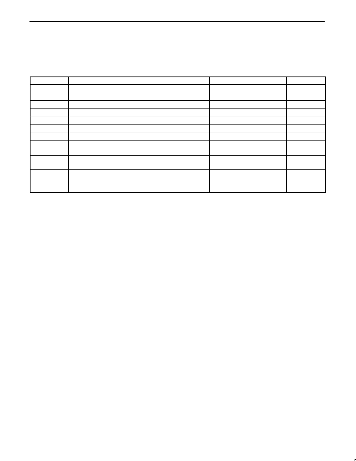
ORDERING INFORMATION
DESCRIPTION TEMPERATURE RANGE ORDER CODE DWG #
16-Pin Ceramic Dual In-Line Package (CERDIP) 0 to +70°C MC3410F 0582B
16-Pin Ceramic Dual In-Line Package (CERDIP) 0 to +70°C MC3410CF 0582B
Philips Semiconductors Linear Products Product specification
MC3410,
MC3410C
10-Bit high-speed multiplying D/A converter
August 31, 1994
744
ABSOLUTE MAXIMUM RATINGS
TA=+25°C unless otherwise noted
SYMBOL
PARAMETER RATING UNIT
V
CC
Power supply +7.0 V
DC
V
EE
-18 V
DC
V
I
Digital input voltage +15 V
DC
V
O
Applied output voltage 0.5, -5.0 V
DC
I
REF(16)
Reference current 2.5 mA
V
REF
Reference amplifier inputs VCC, V
EE
V
DC
V
REF(D)
Reference amplifier differential inputs 0.7 V
DC
T
A
Operating ambient temperature range
MC3410, 3410C
0 to +70 °C
T
J
Junction temperature, ceramic
package
+150 °C
P
D
Maximum power dissipation,
TA=25°C (still-air)
1
F package 1190 mW
NOTES:
1. Derate above 25°C, at the following rates:
F package at 9.5mW/°C
Philips Semiconductors Linear Products Product specification
MC3410,
MC3410C
10-Bit high-speed multiplying D/A converter
August 31, 1994
745
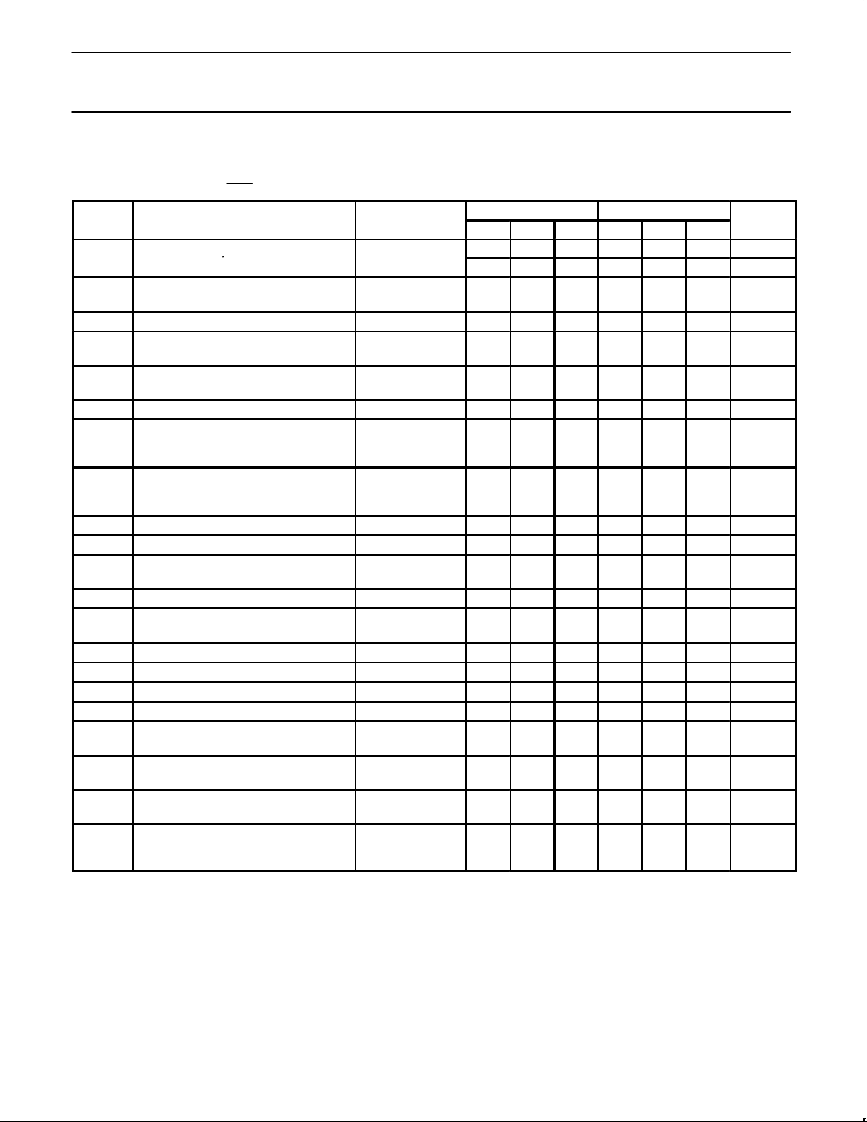
ELECTRICAL CHARACTERISTICS
VCC=+5.0VDC, VEE=-15DC,
V
REF
R16
=2.0mA, all digital inputs at high logic level. MC3410 Series: TA=0°C to +70°C, unless otherwise noted.
TEST CONDI-
MC3410 MC3410C
SYMBOL
PARAMETER
TEST CONDI-
TIONS
Min Typ Max Min Typ Max
UNIT
TA=25°C ±0.05 ±0.1 %
E
r
Relative accuracy
(error relative to full-scale I
O
)
1/4 1/2 LSB
TCE
r
Relative accuracy drift
(relative to full-scale I
O
)
2.5 2.5 ppm/°C
Monotonicity Over temperature 10 10 Bits
t
S
Settling time to within ± LSB
(all bits LOW-to-HIGH)
TA=25°C 250 250 ns
t
PLH
t
PHL
Propagation delay time TA=25°C
35
20
35
20
ns
TCI
O
Output full scale current drift 60 70 ppm/°C
V
IH
Digital input logic levels (all bits)
HIGH-level, Logic “1”
LOW-level, Logic “0”
2.0
0.8
2.0
0.8
V
DC
I
IH
I
IL
Digital input current (all bits)
HIGH-level, V
IH
=5.5V
LOW-level, V
IL
=0.8V -0.05
+.04
-0.4
-0.05
+.04
-0.4
mA
I
REF(15)
Reference input bias current (Pin 15) -1.0 -5.0 -1.0 -5.0 µA
I
OR
Output current range 4.0 5.0 4.0 5.0 mA
I
OH
Output current (all bits high)
V
REF
=2.000V,
R
16
=1000Ω
3.8 3.996 4.2 3.8 3.996 4.2 mA
I
OL
Output current (all bits low) TA=25°C 0 2.0 0 4.0 µA
V
O
Output voltage compliance TA=25°C
-2.5
+0.2
-2.5
+0.2
V
DC
SR I
REF
Reference amplifier slew rate 20 20 mA/µs
ST I
REF
Reference amplifier settling time 0 to 4.0mA, ±0.1% 2.0 2.0 µs
PSRR(-) Output current power supply sensitivity 0.003 0.01 0.003 0.02 %/%
C
O
Output capacitance VO=0 25 25 pF
C
I
Digital input capacitance
(all bits high)
4.0 4.0 pF
I
CC
I
EE
Power supply current
(all bits low)
-11.4
+18
-20
-11.4
+18
-20
mA
V
CC
V
EE
Power supply voltage range TA=25°C +4.75
-14.25
+5.0
-15
+5.25
-15.75
+4.75
-14.25
+5.0
-15
+5.25
-15.75
V
DC
Power consumption
(all bits low)
(all bits high)
220
200
380 220
200
380 mW
Relative accuracy
 Loading...