Philips LX8200SA Schematic
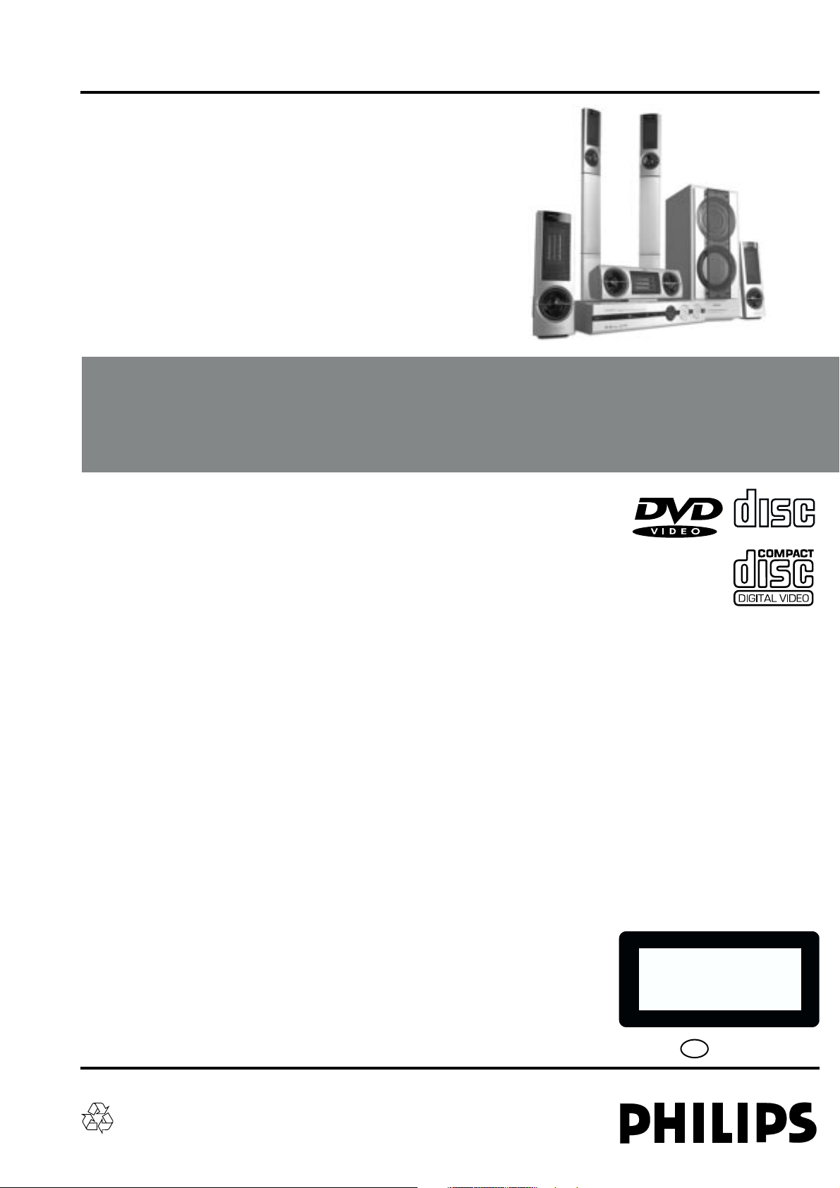
Service Manual
Service
Service
AV System
Service
Service
Service
1. For repair information on the SD4.00SA DVD Module, refer to Service Manual
"DVD Module SD-4.00SA_CH - 3122 785 12480".
2. For repair information on the Subwoofer SW8000SA/00S, refer to Service
Manual "SW8000SA/00S/01S/17S - 3139 785 30099".
LX8200SA/22S
TABLE OF CONTENTS
Page
Location of pc boards & Version variations................1-2
Technical Specifications .............................................1-3
Measurement setup ....................................................1-4
Service Aids, Safety Instruction, etc...........................1-5
Reprogramming of DVD version matrix ..................... 1-7
Setting the TV system default .................................... 1-8
Disassembly Instructions & Service positions .............. 2
Service Test Programs .................................................. 3
Set Block diagram ......................................................4-1
Set Wiring diagram .....................................................5-1
Key & Control Boards ....................................................6
ECO6 Tuner Board : Systems Cenelec..................... 7B
Supply & Main Boards ...................................................8
Power Amplifier Board ................................................... 9
AVC Board ...................................................................10
P-Scan Board .............................................................. 11
Set Mechanical Exploded view & parts list ................. 12
Revision List ................................................................ 13
COMPACT
DIGITAL AUDIO
CLASS 1
©
Copyright 2003 Philips Consumer Electronics B.V. Eindhoven, The Netherlands
All rights reserved. No part of this publication may be reproduced, stored in a retrieval system or
transmitted, in any form or by any means, electronic, mechanical, photocopying, or otherwise
without the prior permission of Philips.
Published by BB 0316 Service Audio Printed in The Netherlands Subject to modification
Version 1.1
LASER PRODUCT
3139 785 30361
GB

SPECIFICATIONS
1-3
GENERAL:
Mains voltage : 110-127V/220-240V Switchable for /21
120V for /37
220-230V for /22
Mains frequency : 50/60Hz
Power consumption : < 0.5W at ECO Power Standby
: < 20W at Standby (DEMO mode off)
: 160W at Active
Clock accuracy : < 4 seconds per day
Dimension centre unit : 390 x 73 x 360mm
TUNER:
FM
Tuning range : 87.5-108MHz
Grid : 50kHz
100kHz for /37
IF frequency : 10.7MHz ± 25kHz
Aerial input : 75 ohm coaxial
Sensitivity at 26dB S/N : < 7uV
Selectivity at 600kHz bandwidth : > 25dB
Image rejection : > 25dB
Distortion at RF=1mV, dev. 75kHz : < 3%
-3dB Limiting point : < 8uV
Crosstalk at RF=1mV, dev. 40kHz : > 18dB
MW
Tuning range : 531-1602kHz
530-1700kHz for /21/37
Grid : 9kHz
10kHz for /21/37
IF frequency : 450kHz ± 1kHz
Aerial input : Frame aerial
Sensitivity at 26dB S/N : < 4.0mV/M
Selectivity at 18kHz bandwidth : > 18dB
IF rejection : > 45dB
Image rejection : > 28dB
Distortion at RF=50mV, M=80% : < 5%
AUDIO INPUTS / OUTPUTS:
Input sensitivity
Aux in (at 1kHz) : 880mV ± 3dB
TV in (at 1kHz) : 350mV ± 3dB
Output sensitivity
Line out (Left/Right) : 0.6V ± 2dB at 100 kohm
Center out (Vol. Max.) : 500mV ± 2dB at 47 kohm
Subwoofer out (Vol. Max.) : 0.76V ± 2dB at 47 kohm
Headphone output at 32 ohm : 660mV ± 2dB (Vol. Max.)
VIDEO OUTPUTS:
All output terminals to be terminated with 75 ohm.
CVBS Out
CVBS Level : 1Vpp ± 0.1V
Luminance S/N : >=45dB (unweighted)
S-Video Out
Y Level : 1Vpp ± 0.1V
Y S/N : >=48dB (unweighted)
C Level (burst) : 286mVpp +1/-4dB
RGB / YUV Out
Amplitude : 0.7Vpp ± 0.1V
S/N : >=50dB (unweighted)
DIGITAL INPUT / OUTPUT:
To be terminated with 75 ohm.
Digital in : IEC 60958
Digital out : SPDIF Coaxial
AMPLIFIER:
Output power (6 ohm, 1kHz, 10% THD)
L & R, Center, Surround : 40W RMS / channel
Amplifier Frequency Response (-3dB) : 250Hz-32kHz
SURROUND : Multichannel, Stereo, 3D Sound
SOUND : JAZZ, ROCK, DIGITAL, CLASSIC
[DRAMA, ACTION, SCI-FI, CONCERT]
[.....] Sound effect available when playing a DVD/VCD disc.

1-7
Caution:
This information is confidential and may not be distributed. Only a qualified service person should
do the reprogramming.
After replacement/repair, the customer settings and also the region code may be lost.
Reprogramming will put the set back in the state in which it has left the factory, i.e. with the default settings
and the allowed region code.
Reprogramming will be done by way of the Remote Control.
Complete version matrix to be enter is
'PLAY 159 XXX XXX XX PLAY'
.
Do the following steps with the Remote Control:
1) Ensure no disc is loaded in the tray.
2) Set the Remote Control to
DISC
source.
3) Press
<PLAY>
followed by numerical keys
<1> <5> <9>
Remark: Top left hand corner of the TV screen will display "
X"
for all these 4 keys that you have pressed.
4) Press now the following numerical keys (8 digits version matrix):
Remark: Nothing will be displayed on the TV screen for all these 8 digits that you have pressed.
for LX8200SA/22S :
<2> <2> <2> <0> <3> <7> <0> <8>
5) Press
<PLAY>
again.
Caution: Wait for about 3 seconds for the set to reset to the required setting.
The TV screen will turn blue follow by a loud sound at the speaker output.
6) Disconnect mains to ensure proper reset.
How to check the version matrix and the software version number of the set:
1) Power up the set and select
DISC
source.
2) Press
<SYSTEM MENU>
on the Remote Control to enter the User Preference Manual (UPM),
follow by pressing the following key:
-
<Cursor Down>
key 4 times
-
<Cursor Right>
key 1 time
-
<Cursor Down>
key 4 times
3) Message "(C)PHILIPS 01- 02 5580 W.WW.WW ...... PXXXXXXXX Y.YY.Y" will be displayed
on the TV screen:
W.WW.WW - indicate the BEA software version number
PXXXXXXXX - indicate the version matrix programmed
Y.YY.Y - indicate the FEA (servo) software version number
4) Press
<SYSTEM MENU>
on the Remote control to exit.
Reprogramming of DVD version matrix

Setting the TV system default
1-8
1) Press
2) From the User Preference Manual on the TV screen, select
<SYSTEM MENU>
accordingly as shown in the table below:
on the Remote Control to enter the User Preference Manual (UPM).
Version Region TV system default
/21R Region 3 AUTO
/21S Region 4 NTSC
/22S Region 2 PAL
/30S Region 4 AUTO
/33S Region 3 AUTO
/37S Region 1 NTSC
3) Press
<SYSTEM MENU>
on the Remote control to exit.
TV SYSTEM
to change the TV system default
DISMANTLING INSTRUCTIONS
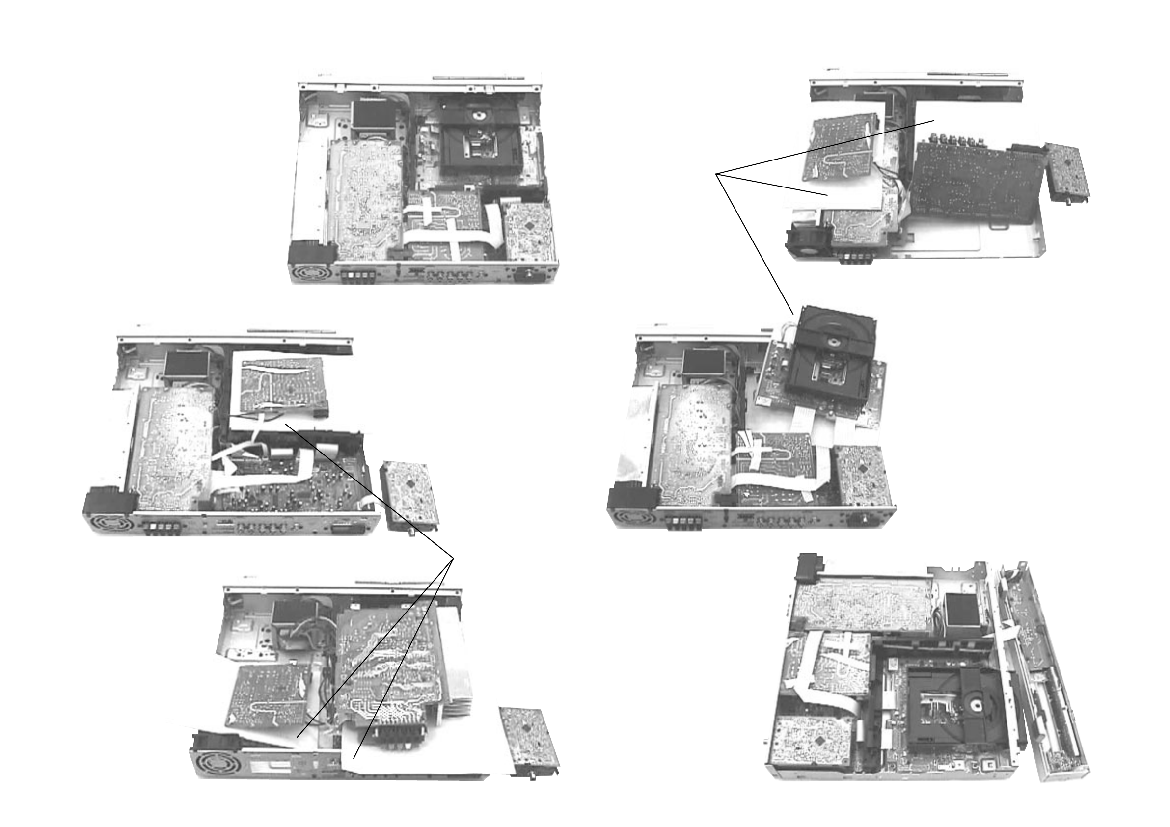
2-1 2-1
Dismantling of the Tuner Board and Main Board and AVC Board
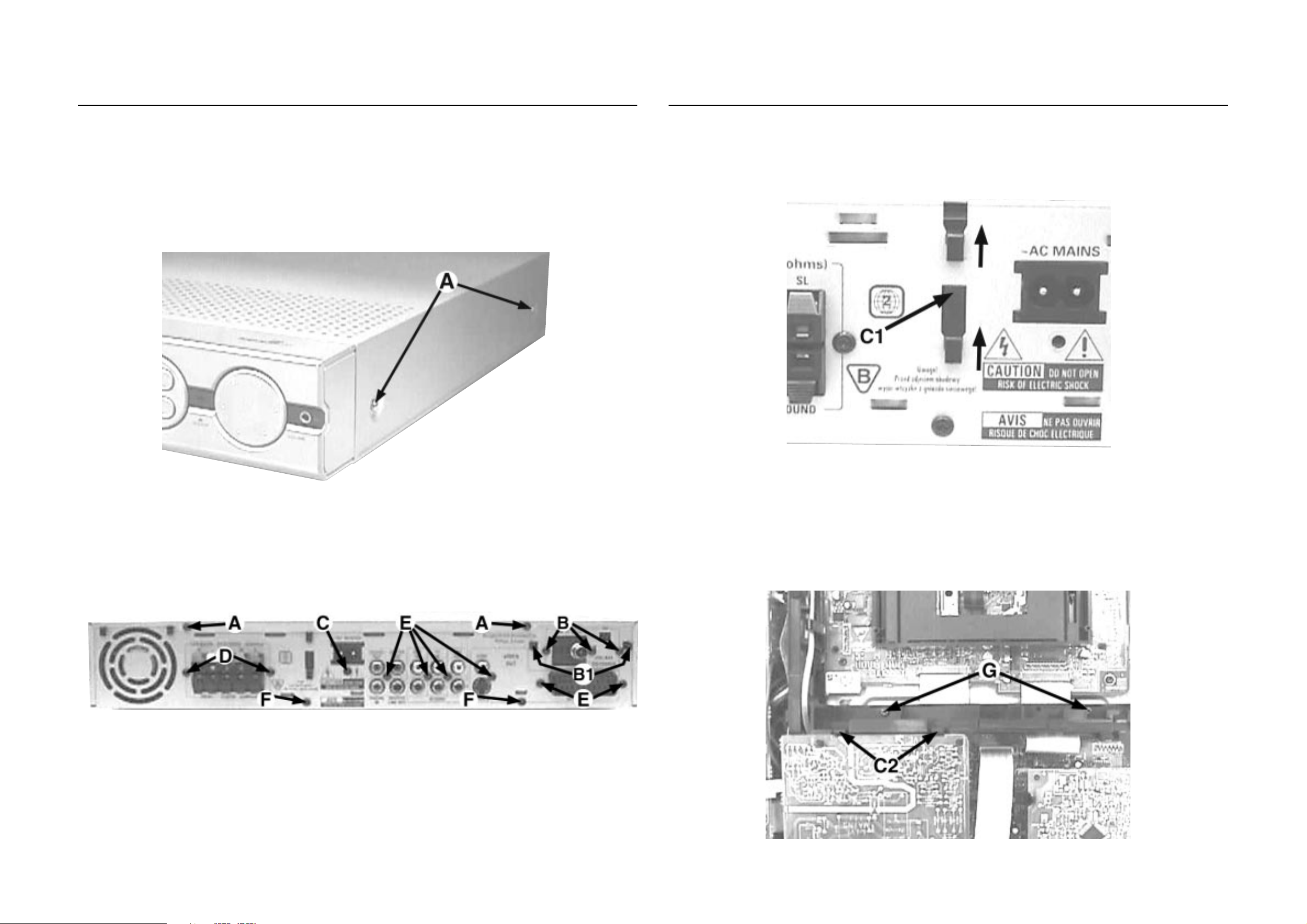
1) Loosen 6 screws A to remove the Cover Top (pos 260).
- 2 screws each on the left & right side (see Figure 1)
- 2 screws on the rear (see Figure 2)
- See Service position A
2) Remove 3 screws B and uncatch 2 catches B1 (see Figure
2) to loosen the Tuner Board (pos 1101).
Dismantling of the Tuner Board and Main Board and AVC Board
3) Remove the Bracket PCB Mains (pos 259) by pressing
the catch C1 inward and slide it up in the direction as
shown in Figure 3.
4) Remove 1 screw C (see Figure 2) and uncatch 2 catches
C2 (see Figure 4) to loosen the Main Board (pos 1104-B).
- See Service position B
Figure 1
Figure 2
5) Remove 2 screws G (see Figure 4) to loosen the Bracket
AV PCB (pos 255).
Figure 3
6) Remove 6 screws E and 2 screws F (see Figure 2) to
loosen the Plate Rear (pos 251) and AVC Board (pos
1102).
- See Service position D
Figure 4
DISMANTLING INSTRUCTIONS
2-2
2-2
Dismantling of the Supply Board and Power Amplifier Board
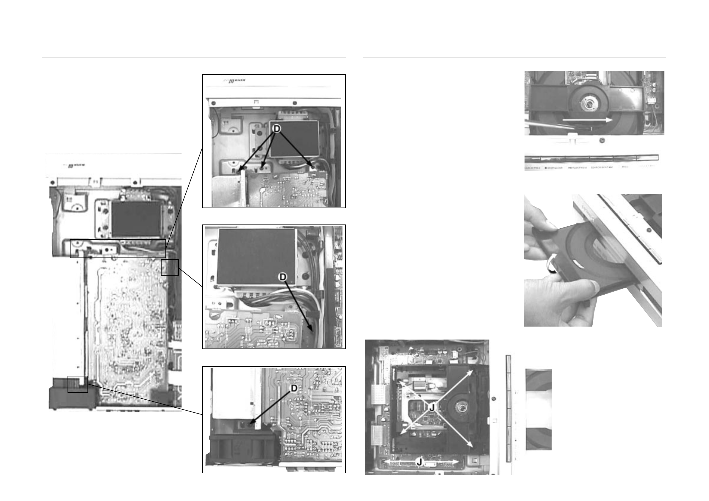
1) Remove 7 screws D to loosen the Supply Board (pos
1104-A) and Power Amplifier Board (pos 1103).
- 2 screws on the Plate Rear (see Figure 2)
- 5 screws on the Plate Bottom (see Figure 5, 6, 7 & 8)
- See Service position C
Dismantling of the DVD Module
1) Use a Flat Head screw driver to give a push in the
direction as shown in Figure 9 to unlock the DVD Tray
before sliding it out.
Figure 9
2) Slide out the DVD Tray and remove the Cover Tray DVD
(pos 105) as shown in Figure 10.
Figure 6
Figure 5
3) Slide out the DVD Tray fully and remove 6 screws J (see
Figure 11) to loosen the DVD Module (pos 1109).
- See Service position E
Figure 10
Figure 7
Figure 11
Figure 8
DISMANTLING INSTRUCTIONS
2-3 2-3
Dismantling of the Front Panel Assembly
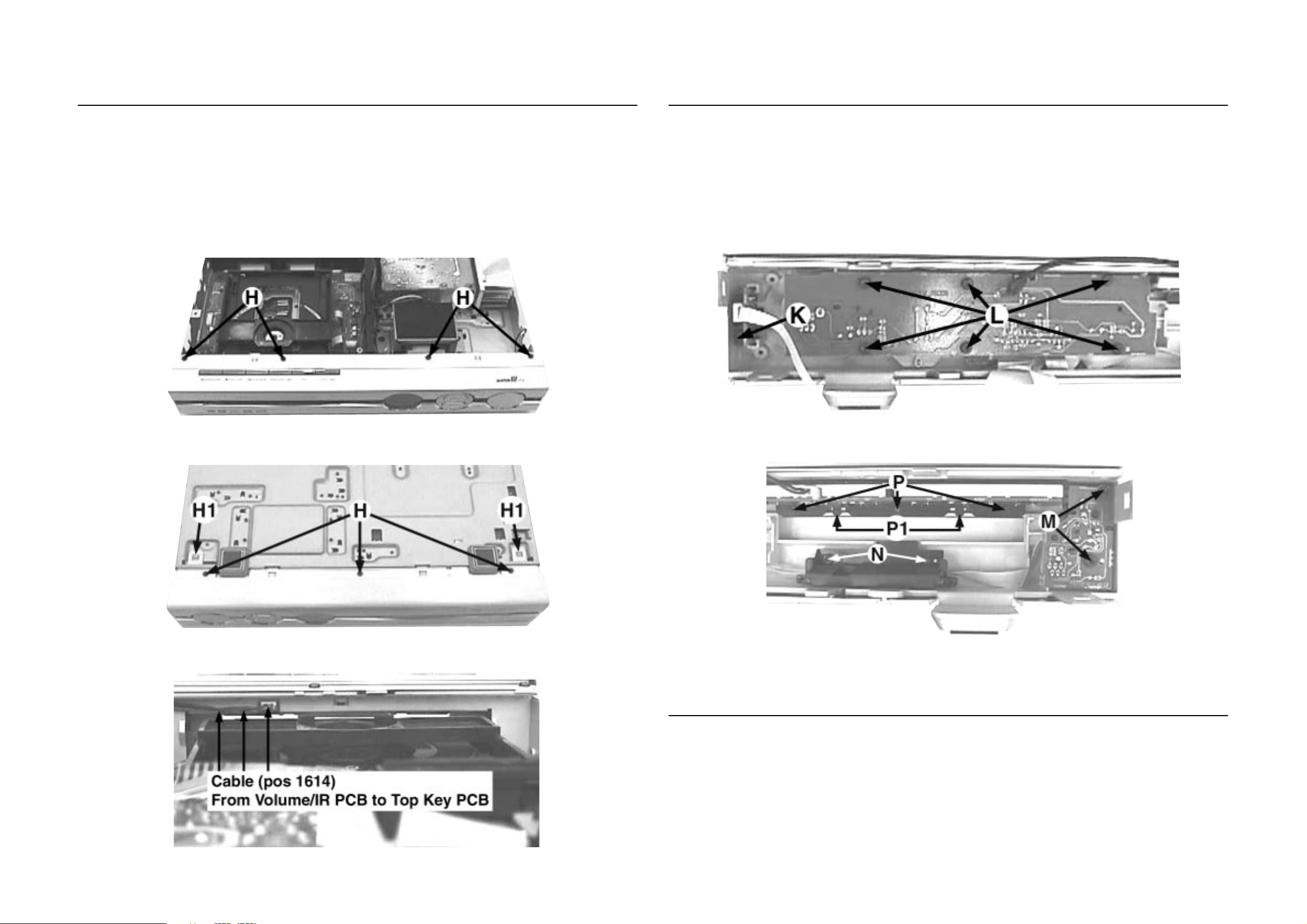
1) Remove 7 screws H (see Figure 12 and Figure 13) and
uncatch 2 catches H1 (see Figure 13) to loosen the Front
Panel Assembly from the set.
- 4 screws on top of the Front Panel Assembly
- 3 screws and 2 catches H1 at the bottom of the Front
Panel Assembly
- See Service position F
2) Make sure to unplug the cable (if obstructed) before
separate the Front Panel Assembly from the set (see
Figure 14).
Dismantling of the Key & Control Boards
1) Remove 1 screw K (see Figure 15) to loosen the
Headphone Board (pos 1105-D).
2) Remove 6 screws L (see Figure 15) to loosen the
Volume& IR Board (pos 1105-C).
3) Remove 2 screws M (see Figure 16) to loosen the Power
On/Off Board (pos 1105-A).
4) Remove 2 screws N (see Figure 16) to loosen the
Bracket LED SACD (pos 109) and SACD LED Board
(pos 1105-B).
5) Remove 3 screws P (for LX8000SA 2 screws only) and
uncatch 2 catches P1 (see Figure 16) to loosen the Top
Key Board (pos 1105-E).
Figure 12
Figure 13
Figure 15
Figure 16
Repair Hints
Figure 14
1) During repair it is possible to disconnect the ECO6 Tuner
Board completely unless the fault is suspected to be in
that area. This will not affect the performance of the rest
of the set.
2) The flex cables are very fragile, care should be taken not
to damage them during repair. After repair, be very sure
that the flex cables are inserted properly into the flex
sockets before encasing, otherwise faults may occurs.
DISMANTLING INSTRUCTIONS
2-4 2-4
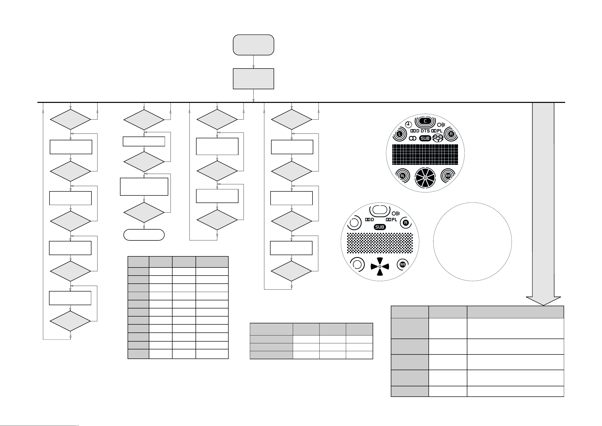
Service position A
Service position B
Service position D
Use a insulation sheet to
prevent any damaged or
short-circuit of the boards.
Service position E
Service position C
Use a insulation sheet to
prevent any damaged or
short-circuit of the boards.
Service position F
3-1
3-1
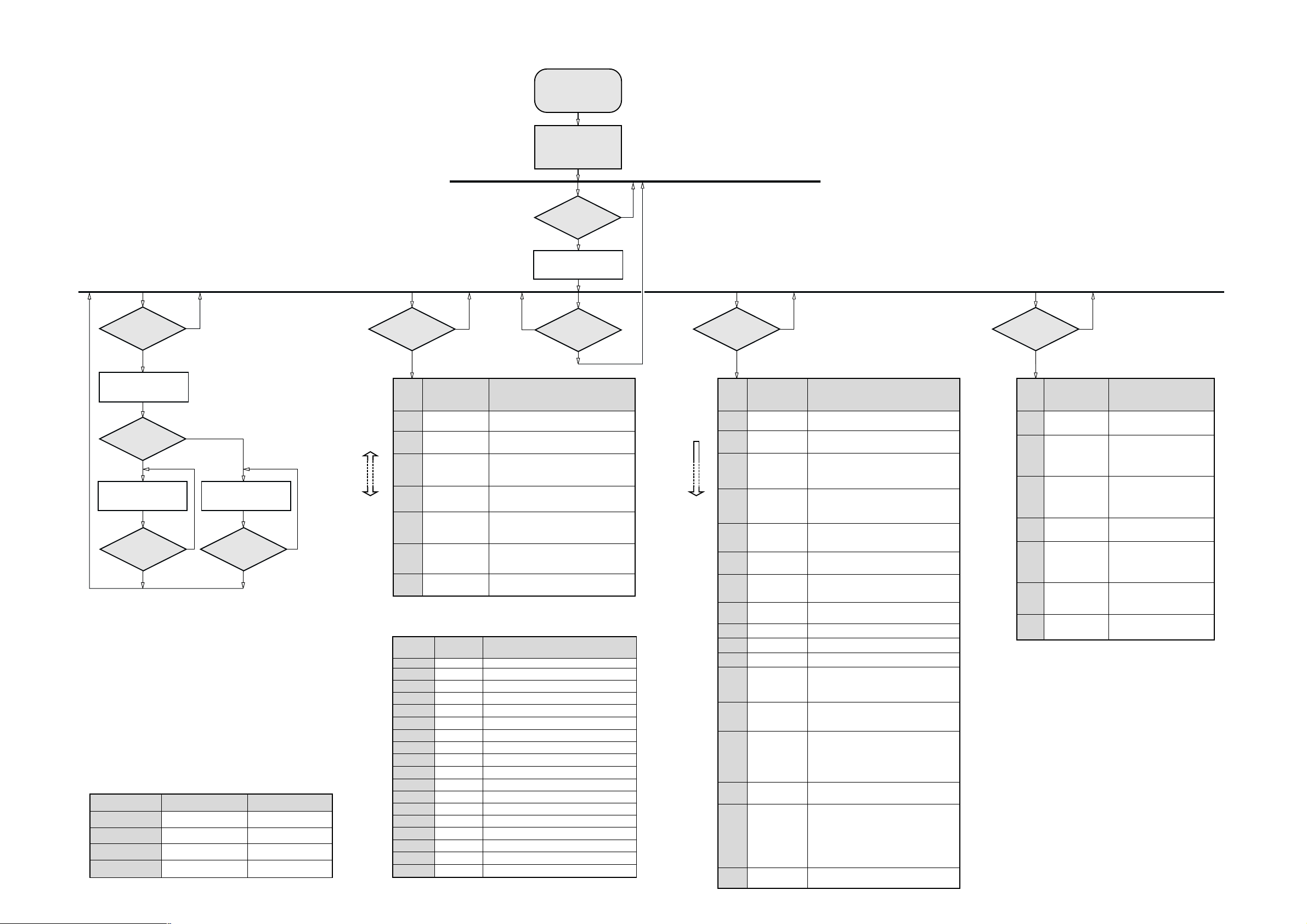
SERVICE TEST PROGRAM
ADC
TEST
SOURCE
Button pressed?
Y
Display shows
"ADC1 Value"
(Input Line - Key0)
SOURCE
Button pressed?
Y
Display shows
"ADC2 Value"
(Input Line - Key1)
SOURCE
Button pressed?
Y
N
N
N
TUNER
TEST
PROG
Button pressed?
Y
Display Tuner Version
"ccc"
PROG
Button pressed?
Y
Service frequencies are
copied to the RAM (see Table 1)
Tuner works normally except:
PROGRAM button
Disconnect
Mains cord ?
Y
Service Mode left
To start service test program
QUARTZ
TEST
N
N
N
CLOCK/TIMER
Button pressed?
Y
Display shows
32K
Output on Quartz-Test-Pin
pin 19 of uP = 2048Hz
CLOCK/TIMER
Button pressed?
Y
Display shows
12M
Output on Quartz-Test-Pin
pin 19 of uP = 2,929.6875Hz
9
Button pressed?
Y
N
& SOURCE
hold T
depressed while
plugging in the mains cord
Display shows the
ROM version
"S-Vyy"
(Main menu)
N
N
S refers to Service Mode
V refers to Version
yy refers to Software version number of the uProcessor
(counting up from 01 to 99)
DISPLAY
TEST
BII
Button pressed?
Y
Display shows Figure 1
and switch all LEDs on
(see Table 2 - Pattern 1)
BII
Button pressed?
Y
Display shows Figure 2
and switch alternate LEDs on
(see Table 2 - Pattern 2)
BII
Button pressed?
Y
N
N
N
Figure 1
Display shows
"ADC3 Value"
(Input Line - AmNTC)
SOURCE
Button pressed?
Y
Display shows
"ADC4 Value"
(Input Line - Option)
9
Button pressed?
Y
ADC Test is used for checking the ADC inputs
to the microprocessor.
The display shows an ADC value between 0
and 255 for an input signal between 0 and 5V.
Note :
If the ADC value on the NTC line is below 69,
the set will go to standby mode because the
temperature is too high.
N
N
PRESET
1
2
3
4
5
6
7
8
9
10
11
Europe
"EUR"
87.5MHz
108MHz
531kHz
1602kHz
558kHz
1494kHz
87.5MHz
87.5MHz
87.5MHz
87.5MHz
98MHz
USA
"USA"
87.5MHz
108MHz
530kHz
1700kHz
560kHz
1500kHz
98MHz
87.5MHz
87.5MHz
87.5MHz
87.5MHz
Oversea
"OSE"
87.5MHz
108MHz
531/530kHz*
1602/1700kHz*
558/560kHz*
1494/1500kHz*
87.5/98MHz*
87.5MHz
87.5MHz
87.5MHz
98/87.5MHz*
Table 1
Note: * Depending on the selected grid frequency (9 or 10kHz).
By holding the "SOURCE" and "PROG" buttons depressed
while switching on the Mains supply, the tuning grid frequency
is toggled between 9kHz and 10kHz for the Oversea (/21)
version.
Display shows Figure 3
and switch all LEDs off
(see Table 2 - Pattern 3)
Button pressed?
LEDs
SACD
STANDBY / ECO POWER
LCD BACKLIGHT
Pattern 1
ON
GREEN
ON
Table 2
N
Figure 2 Figure 3
Various
other Tests
ACTION
"PASS" is displayed if the uProcessor read back
the test pattern correctly, otherwise "FAIL" will be
displayed.
Load default data. Display shows "NEW" for 1 second.
Caution!
All presets from the customer will be lost!!
Pressing this button will toggle between the status
"AUTO STANDBY ON" and "AUTO STANDBY OFF".
Pattern 2
OFF
RED
ON
Pattern 3
OFF
OFF
ON
TEST
EEPROM TEST A test pattern will be sent to the EEPROM.
Activated with
T
9 to Exit
EEPROM FORMAT
TEST
AUTO STANDBY
TOGGLE
S
CENTER -
(RC)
The status will scroll once across the Display.
ROTARY
ENCODER TEST
Rotary Volume
Knob
Display shows value for 2 seconds.
Values increases or decreases in steps of 1 until
9
Y
0 (Volume Min.) or 40 (Volume Max.) is reached.
LEAVE SERVICE
TEST PROGRAM
Disconnect
mains cord
LX7000SA & LX8000SA_Service Test Program_dd wk0232
3-2 3-2
SERVICE TEST PROGRAM
DVD IIC
COMMUNICATION
TEST
MUTE (RC)
Button pressed?
Y
Send request for
DVD Software Version
via IIC ports
Software Version
Received?
Y
Display shows
"DVD/www/xx.yy.zz"
9 (RC)
Button pressed?
Y
DVD IIC Communication Test is used to test the IIC communication port
between the DVD module and the microprocessor of the set.
www : refer to BEA Software version.
BEA = Back End Application (DVD Application Software).
xx.yy.zz : refer to Basic Engine Software version.
Basic Engine = part of the DVD module controlling the servo.
ERROR CODE (Faulty Modules)
ERROR CODE
00
01
10
11
N
N
Display shows
N
Button pressed?
BASIC ENGINE PART
OK
OK
Faulty
Faulty
Table 3
"FAIL"
9 (RC)
Y
STI + PERIPHERALS
N
OK
Faulty
OK
Faulty
Remote Control (RC) must be in DVD source
before start of any DVD Service Test.
DVD VERSION
MATRIX INFO
N
DISPLAY
SLASH ’###’
REGION ’#’
MULANG ’US/AP’
or
MULANG ’US/EU’
ASLANG ’#’
MULTI-CH ’YES’
or
MULTI-CH ’NO’
SMARTPIC ’YES’
or
SMARTPIC ’NO’
Choose step
by pressing
S
(RC)
T
(RC)
"DIM" (RC)
Button pressed?
Y
STEP
1
2
3
4
5
6
DVD Version Matrix Info is used to read the version matrix information
that are stored/defined in the DVD module software.
ERROR CODE (Nucleaus)
ERROR
CODE
0601
1101
1102
1103
1104
1201
1202
1203
1204
1301
1302
1303
1304
1601
5401
5402
5403
5403
NUCLEUS
NUMBER
6
11
-
-
-
12
-
-
-
13
-
-
16
54
-
-
-
To start service test program
& SOURCE
hold T
depressed while
plugging in the mains cord
Display shows the
ROM version
"S-Vyy"
(Main menu)
DVD SERVICE
TEST
DISC (RC)
Button pressed?
Y
Display shows
"DVD SERVICE"
N
9 (RC)
Button pressed?
Y
INFORMATION
Slash version number
Region code setting (Number 1 - 6)
Menu language table :
US/AP (USA-Asian Pacific language table)
US/EU (USA-Europe language table)
Audio/Subtitle language table
(Number 1 - 4)
Available of multichannel decording
Available of smart picture
Press 9 (RC) to exit
ERROR
DESCRIPTION
Calculated Checksum of FLASH is not correct
I2C bus busy before start
NVRAM access time-out
No NVRAM acknowledge
NVRAM reply time-out
I2C bus busy
Error sending I2C command to Slave
Slave controller not responding
Slave response is not correct
Parity error receiving data from Basic Engine
Parity error sending data to Basic Engine
No communication with Basic Engine
Comunication time-out with Basic Engine
The SDRAM is faulty
I2C bus busy
Error sending I2C command to Scart Switch IC
Scart switch IC not responding
Scart switch IC response is not correct
Table 4
N
S refers to Service Mode
V refers to Version
yy refers to Software version number of the uProcessor
(counting up from 01 to 99)
DVD PLAYER
TEST
N
DISPLAY
BAR
PICTURE
PINK
NOISE
SCART
LOOP DVD
SCART
LOOP EXT
SINE
SOUND
ENG"xx.yy.zz"
TRAY
SLEDGE
MOTOR
FOCUS
RADIAL
GROOVES
TRAY
LO"wwxxyyzz"
ERROR
"BITS xx"
"aa-bbb
cccc"
Go to next
step
by pressing
T
(RC)
"VOL +" (RC)
Button pressed?
Y
STEP
1**
2**
3A**
3B**
4**
5
6
7
8**
9**
10**
11
12
13
14
15
ACTION
Output of a test picture on all available video
output devices.
Output of noise on all channels available.
Output of internally generated pink noise on all
channels available, test picture (internally
generated Colour Bar) on screen.
Press
S
(RC) to go to Step 3B.
Output of internally generated pink noise on all
channels available, test picture (external signal)
on screen.
Press
T
(RC) to return to Step 3A.
Sine sound output on all channels available.
The sound can be stopped by pressing the
"STOP"(RC) button.
Returns the Software Version of the basic
engine.
The user can move the tray in and out by
pressing "PLAY"(RC) or "RESUME"(RC) button.
User can insert or remove a disc.
The user can move the sledge in and out by
pressing "PLAY"(RC) or "RESUME"(RC) button.
The disc motor starts to run.
Focus Test.
Radial Test.
The laser spot jumps to another position.
Press "PLAY"(RC) to jump to the next position.
Press "RESUME"(RC) to jump to the previous
jump position.
The user can move the tray in and out by
pressing "PLAY"(RC) or "RESUME"(RC) button.
User can insert or remove a disc.
Reads out info from the error log (8 hex digits).
Up to 16 errors can be stored in a buffer.
The elements can be selected by pressing the
"PLAY"(RC) or "RESUME"(RC) button.
If the error log does not contain any fault codes,
"LO-00000000" will be displayed.
Shows all error bits. Selects the error bit by
pressing "PLAY"(RC) or "RESUME"(RC) button.
Runs the Dealer Test infinitely. The information
returned from the module will be displayed.
The loop number indicates the number of times
the loop test has been performed.
aa - Error Code Faulty Modules (see Table 3)
bbb - Loop Number
cccc - Error Code Nucleaus (see Table 4)
Disconnect mains cord to exit the Service Test
Program.
DVD DEALER
TEST
"VOL -" (RC)
Button pressed?
N
Y (Execute all the tests below without interaction)
STEP
1
2
3
4
5
6
DISPLAY
CHECKSUM
FLASH
S2B
ECHO
IIC
NVRAM
NVRAM
WRITE
SDRAM
WRITE
ALL TEST FAIL
or
ALL TEST PASS
ACTION
Check the correctness of the
checksum of the flash.
S2B Echo Mode.
(This test is executed very fast
and hence user will not be able
to see this display message)
Check the correctness of the
IIC bus to the NVRAM.
(This test need about 3 minutes
to perform)
Check writing to the NVRAM.
Check writing to the SDRAM.
(This test is executed very fast
and hence user will not be able
to see this display message)
Result of all the tests.
Disconnect mains cord to exit
the Service Test Program.
DVD Dealer Test is used to check the flash RAM, the SDRAM,
the DRAM, the NVRAM and the I2C communication.
When all the tests are passed, display shows "ALL TEST PASS".
If at least one of the test fails, display shows "ALL TEST FAIL".
DVD Player Test is used to start several DVD specific tests.
At the end of the test, an error code "aa-bbb cccc" (see Step15) will be
shown that indicates which module(s) failed.
** User has to give a confirmation by triggering one of the following:
- If the test is OK, press "PLAY"(RC) button then follow by T (RC)
button to go to the next step.
- If the test is not OK, press "RESUME"(RC) button then follow by
T (RC) button to go to the next step.
Note : By pressing only the T (RC) button to go to the next step without
triggering a confirmation, the test will be assume as OK by default.
Equipment required to run the DVD Player Test:
- television set
- 6 audio speakers
- an external video source
LX7000SA & LX8000SA_Service Test Program_dd wk0232
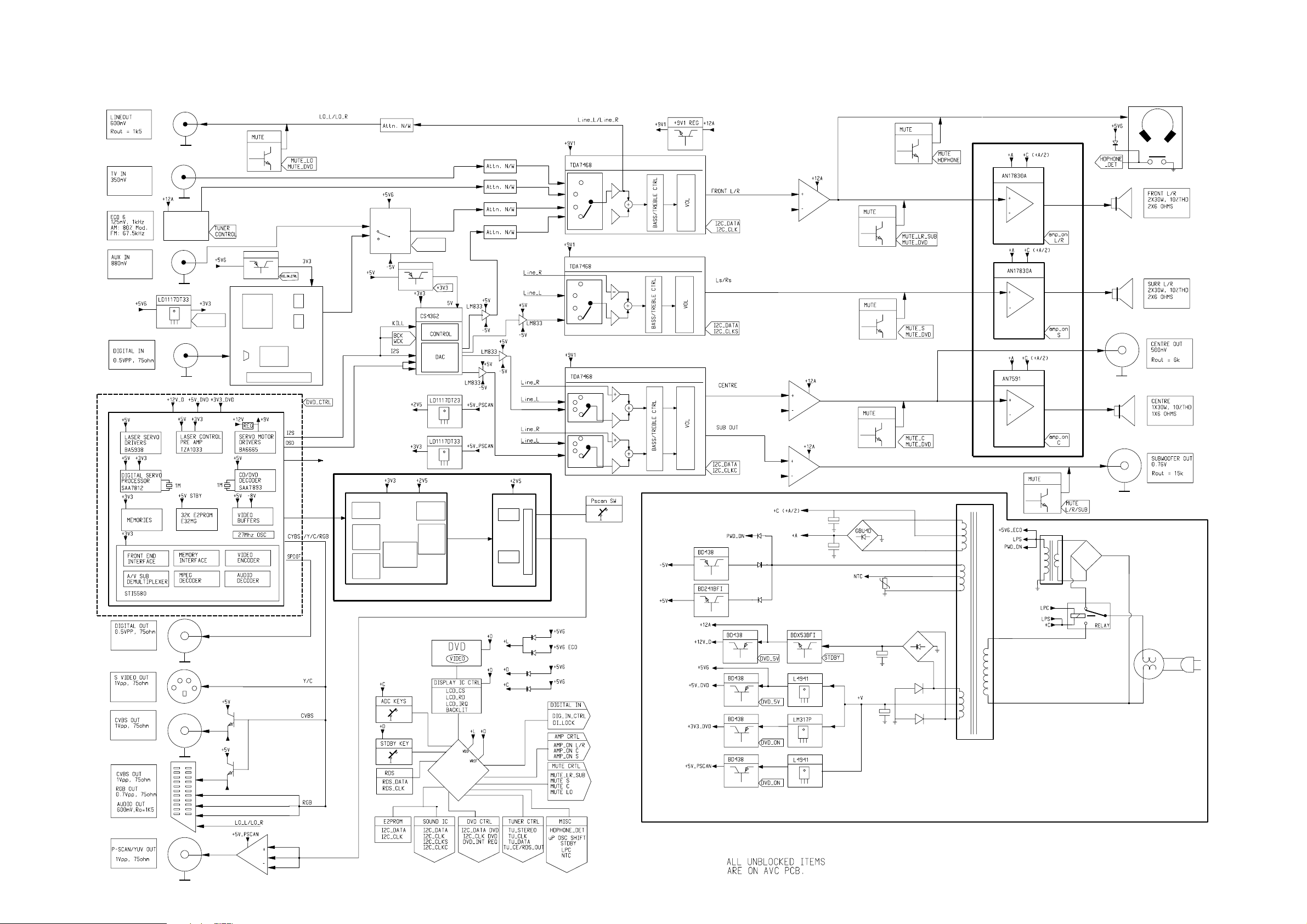
SET BLOCK DIAGRAM
FM-95.00
DIG_IN_CTRL
BC369 & LD1117
UDA1351TS
L3-BUS
INTERFACE
IEC958
DECODER
4-1
HEF4053BT
DIG_IN_CTRL
BC369
DAC
DAC
4-1
L/R
POWER AMP
SURROUND
POWER AMP
DVD
CLK & TIMING CIRCUIT
YUV
MUTE_DVD
*
FLI2200
PLL / CLK
GENERATOR
INPUT
SIGNAL
FORMATTER
CONTROL
INTERFACE
& REGISTERS
DEINTERLACER
CORE
SYNC
GENERATOR
OUTPUT
SIGNAL
FORMATTER
ADV7300
STD
DEF
HIGH
DEF
P-SCAN / YUV
OVERSAMPLING
CENTRE
POWER AMP
MAINS TRAFO
*
LPS COIL
SUPPLY
-5V
*
-5V
*
3X
TMP88CU74F
Not in all versions
*
3139 119 34790_Block Diagram (Sheet 130)_dd wk0240
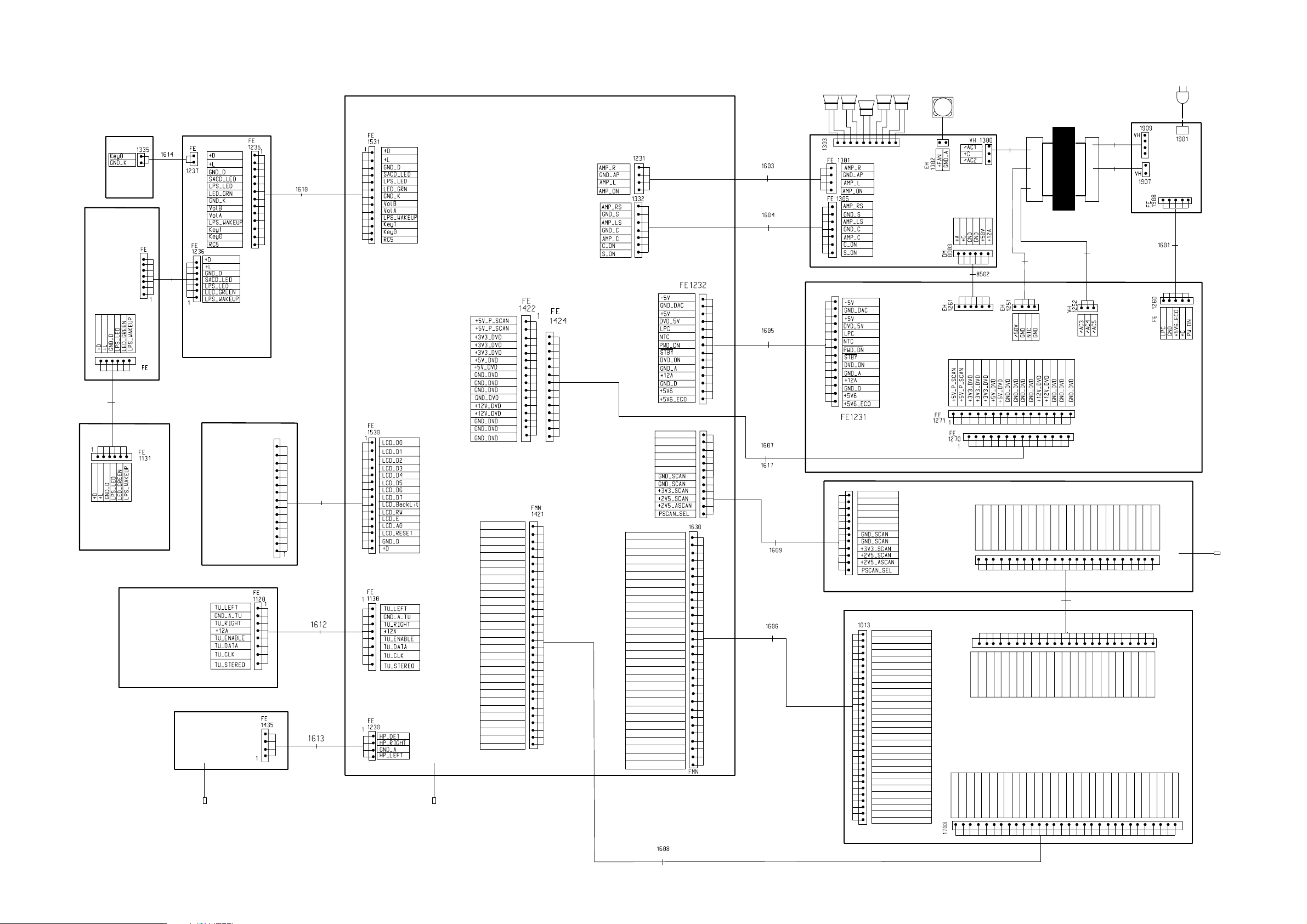
SET WIRING DIAGRAM
5-1
5-1
TOP
KEY
SACD
LED
1
1616
side
1
180mm
2P
1580
1615
7P
120mm
FOLD
side
1581
side
6P 100mm AD FOLD
1
side
AD
side
VOLUME / IR
13P 340mm AD FOLD
side
AVC
L
SL
C
SRR
FAN
0385
TRAFO
1
4P 140mm BD
1
1
7P 140mm BD
1
AMPLIFIER
1
1
180mm
280mm
340mm
340mm
180mm
6P 120mm
1
1
1
***
MAIN
**
side
**
**
1
5P 140mm BD
1
*
1
1
14P 120mm AD FOLD
SUPPLY
1
side
LCD
DISPLAY
POWER
ON / OFF
TUNER
SIDE
HEADPHONE
1820 100mm 1601 100mm
3139 119 34790_Wiring Diagram (Sheet 132)_dd wk0232
BD 15P
380mm
8P 100mm AD
4P 480mm BD
FOLD
I2C_CLK_DVD
I2C_DATA_DVD
SCART1
SCART0
B_REF
B_U
G_REF
G_Y
R_REF
R_V
Y_REF
Y
C_REF
C
CVBS_REF
CVBS
+3V3
+3V3
+5V
+12V
+12V
MUTE_DVD
GND
PCMSCLK(NC)
PCMDATA0(NC)
GND
PCMCLK (NC)
PCMLRCLK(NC)
GND
SPDIF
FOR SET WITH PROGRESSIVE SCAN ONLY
:
*
FOR SET WITH LOW STANDBY
:
**
FOR /21 ONLY
:
***
FE 1423
GND
Y
GND
Pb/Cb
GND
Pr/Cr
1
GND
384FS
GND
DSD_LFE
GND
DSD_CENTRE
GND
DSD_Rs
GND
DSD_Ls
GND
DSD_R
GND
DSD_L
GND
WORD_CLK/SEL_DSD
GND
BIT_CLK/DSD_CLK
GND
256FS
GND
SCL-DAC
SDA-DAC
GND
DSD_PCM8 (NC)
GND
DSD_PCM9(NC)
INT_REQ
DAC_RST
CLK_SEL
30P 100mm BD 1MMP
*
*
16P 260mm AD FOLD
14P 260mm AD FOLD
Side FE 1002
1
1
*
12P 120mm AD
1
30P 100mm BD 1MMP
*
GND
Y
GND
Pb/Cb
GND
Pr/Cr
1
GND
384FS
GND
DSD_LFE
GND
DSD_CENTRE
GND
DSD_Rs
GND
DSD_Ls
GND
DSD_R
GND
DSD_L
GND
WORD_CLK/SEL_DSD
GND
BIT_CLK/DSD_CLK
GND
256FS
GND
SCL-DAC
SDA-DAC
GND
DSD_PCM8 (NC)
GND
DSD_PCM9
P50/GPIO2(NC)
GPIO3
GPIO1(NC)
*
PSCAN
*
C
SDA
SCL
GND
1
Side FMN 1000
1
VSYNC
SCL
SDA
GND
VSYNC
HSYNC
HSYN
*
GND
GND
GND
27MHZ CLK
GND
27MHZ CLK
YC0
1602
*
1704
YC0
GND
GND
YC1
YC1
GND
GND
YC2
GND
YC2
24P 120mm BD 1MM FD
FFC 1MM
YC3
GND
YC3
YC5
+3V3
YC4
+5V
+3.3V
YC5
+3V3
YC4
+5V
DVD SD4-00-SA-CH
GND
I2C_DATA_DVD
I2C_CLK_DVD
1
SCART1
SCART0
B_REF
B_U
G_REF
G_Y
R_REF
R_V
Y_REF
+3V3
C
C_REF
CVBS
CVBS_REF
Y
+3V3
MUTE
+12V
+12V
+5V
+3.3V
GND
YC6
GND
YC6
PCMDATA0(NC)
PCMSCLK(NC)
YC7
YC7
GND
GND
GND
PCMLRCLK
PCMCLK (NC)
GND
SPDIF
1618 70mm
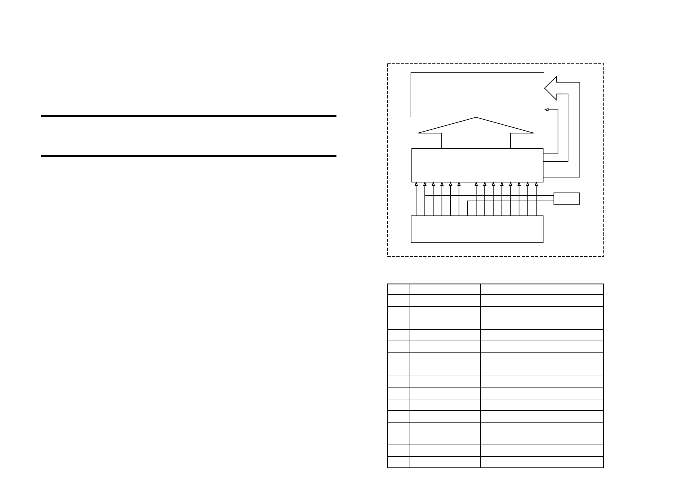
6-1
LCD MODULE
BLOCK DIAGRAM
6-1
LCD PANEL
48 * 15 DOTS with 38 ICONS
C0
C14
.
.
.
.
.
.
.
.
.
KEY & CONTROL BOARDS
TABLE OF CONTENTS
LCD Module - Block diagram .......................................... 6-1
LCD Module - Interface Pin Function .............................. 6-1
Top Key Part - Layout & Circuit diagram ......................... 6-2
SACD LED Part - Layout & Circuit diagram .................... 6-3
Volume & IR Part - Component & Chip layout ................ 6-4
Volume & IR Part - Circuit diagram ................................. 6-5
Headphone Part - Layout & Circuit diagram ................... 6-6
Power ON/OFF Part - Layout & Circuit diagram ............. 6-6
Electrical parts list............................................................ 6-7
S0 S49
.....
.....
.
.
.
.....
.
.....
.
.
.
.....
.
.....
.
.
...
.
.
IC AX6120
5
6
7
8
9
10
11
12
13
14
15
E
VDD
VSS
A0
RESET
LED+
D7
D5RWD4D3D2D1D0
D6
INTERFACE
INTERFACE PIN FUNCTION
NO SYMBOL I/O FUNCTION
1. DB0 I/O Data Bus
2. DB1 I/O Data Bus
C15
C15
C14
.
.
.
.
.
.
.
.
.
C0
LED
1
2
3
4
3. DB2 I/O Data Bus
4. DB3 I/O Data Bus
5. DB4 I/O Data Bus
6. DB5 I/O Data Bus
7. DB6 I/O Data Bus
8. DB7 I/O Data Bus
9. LED+ P Power Supply for LED
10. RW I Read/Write Execution Control
11. E I Read/Write Start Signal
12. A0 I Register Select input
13. RESET I Reset Input Pin
14. VSS (LED-) P GND
15. VDD P Power Supply for Logic
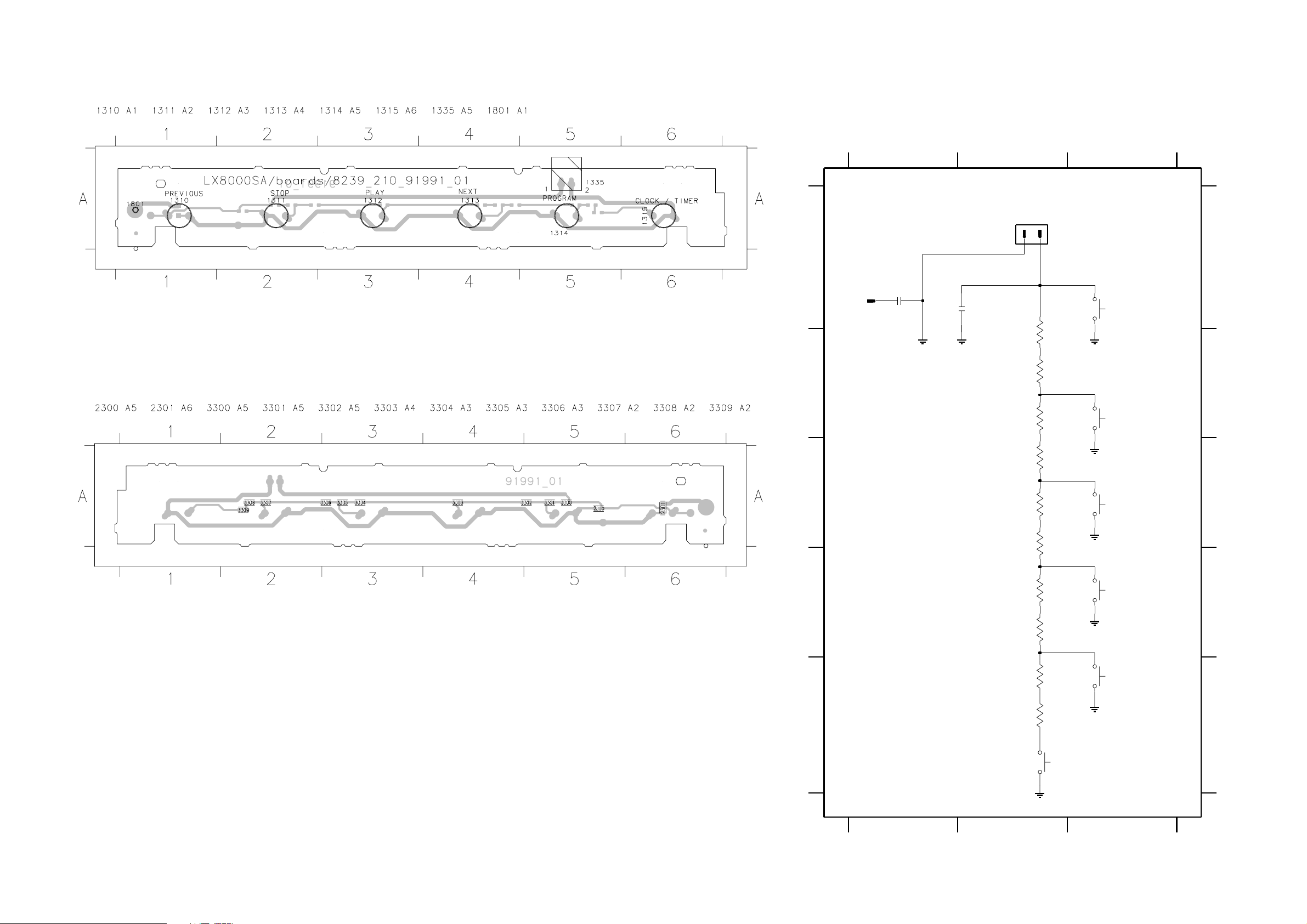
6-26-2
TOP KEY BOARD - CIRCUIT DIAGRAMTOP KEY BOARD - COMPONENT LAYOUT
This assembly drawing shows a summary of all possible versions. For components used in a specific version see schematic diagram and respective parts list.
TOP KEY BOARD - CHIP LAYOUT
3139 113 3481 pt1 dd wk0227
1310 A3
1311 B3
1312 C3
A
B
1313 D3
1314 E3
1315 E2
TOP KEY
RT-01T
1
1801
1335 A2
1801 A1
2300 A1
2301 A1
3300 B2
3301 B2
3302 B2
3303 C2
3304 C2
3305 C2
3306 D2
3307 D2
123
From VOLUME / IR
EH-S
1335
1
2
# 2301
100n
GND_K
2300
33p
GND_K
150R
220R
270R
3300
3302
A
1310
1311
3308 E2
3309 E2
PREV
GND_K
STOP
A
B
This assembly drawing shows a summary of all possible versions. For components used in a specific version see schematic diagram and respective parts list.
3139 113 3481 pt1 dd wk0227
C
D
E
Note :
Some values may varies, see respective
parts list for correct value.
# : Provision
390R
560R
820R
1K2
1K8
2K7
4K7
1315
3303
3304
3306 3305
3307 3301
3308
3309
Clock/ Timer
1313 1312
1314
GND_K
PLAY
GND_K
NEXT
GND_K
Program
GND_K
C
D
E
3139 118 55940...8239_210_91991_01...for 3481 pt1 dd wk0227
123
GND_K
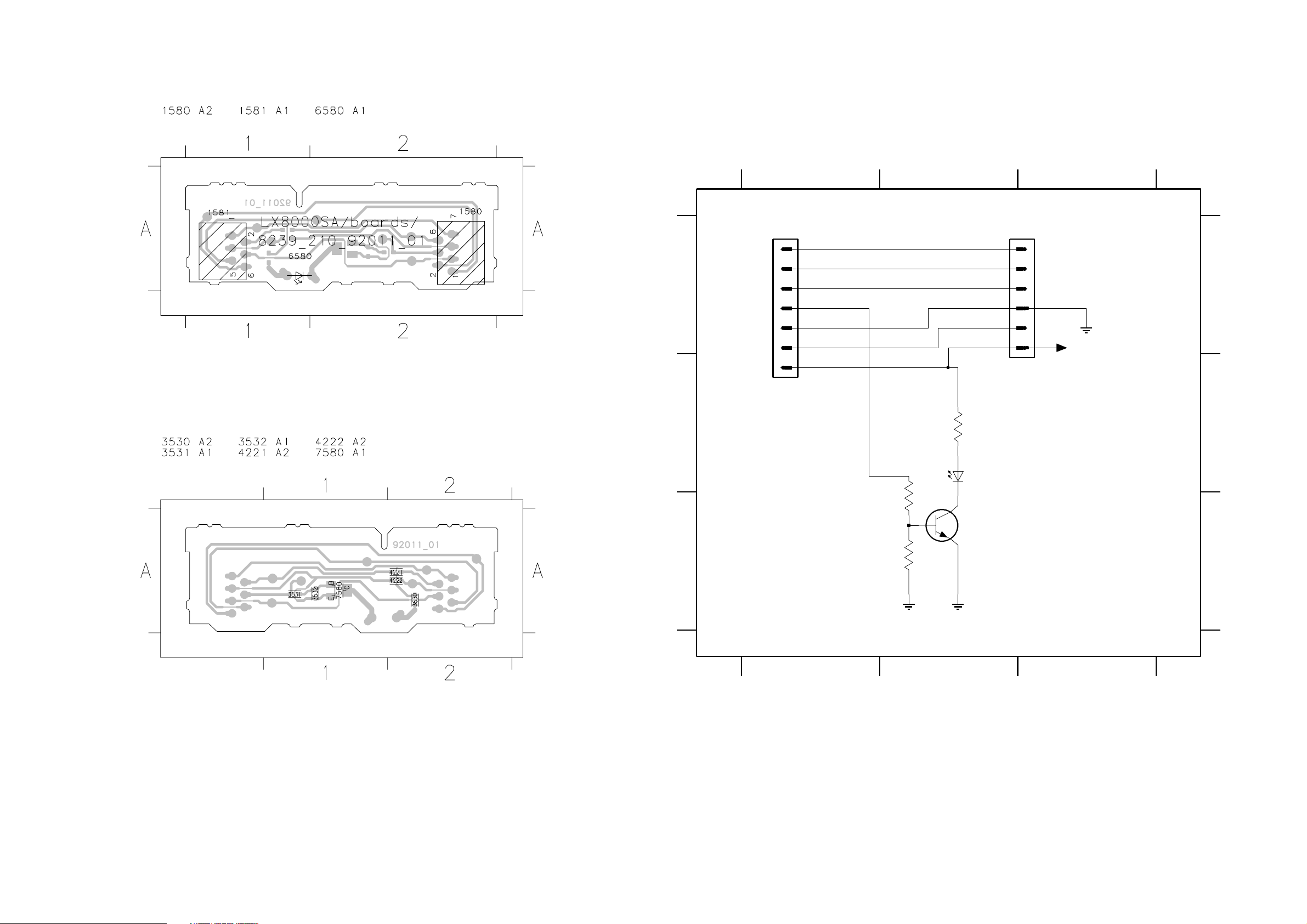
6-3 6-3
SACD LED BOARD - CIRCUIT DIAGRAMSACD LED BOARD - COMPONENT LAYOUT
This assembly drawing shows a summary of all possible versions.
For components used in a specific version see schematic diagram and respective parts list.
SACD LED BOARD - CHIP LAYOUT
3139 113 3481 pt1 dd wk0227
1580 A1 1581 B3 3530 B2
FE-ST-VK-N
1580
1
2
A
3
4
5
From VOLUME / IR
6
7
B
3531 C2 3532 C2
6580 B2 7580 C2
123
SACD LED
LPS_WAKEUP
1581
6
5
4
3
+D
2
1
To POWER ON/OFF
GND_D
SCAD_LED
LED_GRN
3530
LPS_LED
GND_D
+L
+D
FE-ST-VK-N
150R
A
B
This assembly drawing shows a summary of all possible versions.
For components used in a specific version see schematic diagram and respective parts list.
3139 113 3481 pt1 dd wk0227
C
Note : Some values may varies, see respective
parts list for correct value.
123
6580
10K
3531
7580
BC847B
10K
3532
GND_D GND_D
1CHTDK3
C
3139 118 55940...8239_210_92011_01...for 3481 pt1 dd wk0227
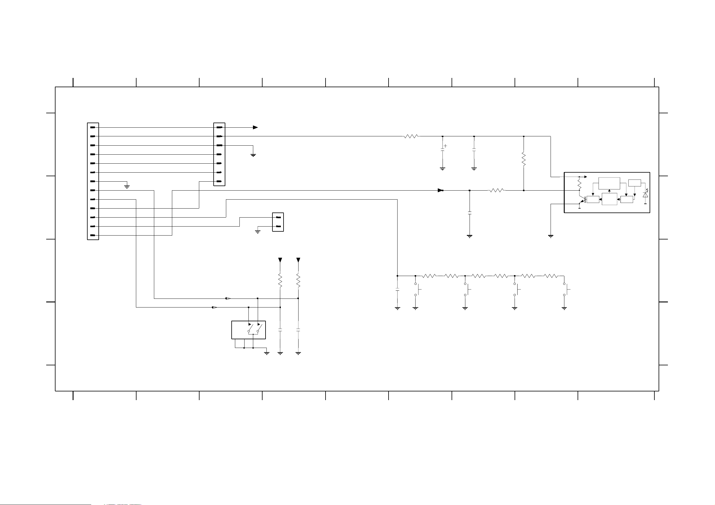
VOLUME & IR BOARD - CIRCUIT DIAGRAM
6-5 6-5
1235 A1 1236 A3 1237 C4 1242 C6
12345678
FE-ST-VK-N
1235
1
2
3
4
5
6
7
8
9
10
11
12
13
To AVC PCB
A
B
+D
+L
GND_D
SACD_LED
LPS_LED
LPS_GRN
GND_K
VolB
VolA
LPS_WAKEUP
Key 1
Key 0
RC5
GND_K
1243 C7 1244 D3 1245 C7 1246 C8 2211 D4 2212 D4 2214 B7 2215 A7 2216 A6 2217 C6 3213 C4 3214 C4 3215 C6 3216 A8 3217 A6 3218 B7 3220 C7 3221 C7
FE-ST-VK-N
1236
7
6
5
4
3
2
To SACD LED
1
+D
GND_D
GND_K
1
2
EH-S
1237
+D
TO TOP KEY
+D
3217
100R
GND_D
RC5
47u
2216
GND_D
GND_D
2n2
2215
47n
2214
3218
1K
3216
10K
VS2
OUT1
GND3
GND_D
3222 C7 3223 C8 3224 C8
9
VOLUME & IR
TSOP2236
DEM
CTRL
CIRCUIT
BAND
PASS
AGC
INP
PIN
7210 A9
A
7210
B
C
D
3222
390R220R
1245
3223
560R
Surround
3224
820R
1246
Sound
GND_KGND_K
3139 118 55940...8239_210_92001_01...for 3481 pt1 dd wk0227
C
D
VolA
VolB
1244
EVE
MT15MT2
4
13
2
GND_D
10K
2211
GND_D
3213
10n
10K
2212
GND_D
3214
10n
2217
GND_K
3215
150R
33p
1242
Source
GND_K GND_K
3220
1243
3221
270R
Open_Close
Note : Some values may varies, see respective parts list for correct value.
12345678 9
 Loading...