


Service
Service
Service
Service
FW-C780
A01 - 157
Service
Product Service Group CE Audio
Service Information
Already published Service Informations :
CORRECTION TO SERVICE MANUAL
*Page 9-5 : Due to some error, the Tape Adjustment & Check Table
*Correction of Mechanical & Accessories parts list (Page 13-2):
Change 0151 3139 118 16070 Cover Cassette Left
Delete 0309, 0310
*Correction of circuit drawing and parts list for Front Control
Board:
Delete 6612
*Correction of circuit drawing and parts list for Front Display
Board:
Add 2508 3198 024 44730 47nF 50V
Change 2536 4822 126 13883 220pF 5% 50V /21/30/37
Delete 3597, 3840, 4417, 4421
*Correction of circuit drawing and parts list for AF9 Board:
Add 2210 4822 126 13879 220nF +80/-20% 16V
Change 2208 4822 126 13879 220nF +80/-20% 16V
Delete 4102, 4118
*Correction of circuit drawing and parts list for MMPWR 100W
Module:
Mains Board
Change 6901 5322 130 81917 SB140 /21
is enclosed.
0152 3139 118 16060 Cover Cassette Right
0152 3139 118 16050 Cover Cass. Right Dolby /34
0153 3139 114 72820 Lens Cassette Left
0154 3139 114 72830 Lens Cassette Right
1503 3139 110 34800 FFC Foil 19P/180/19P BD
5403 2422 543 01069 RES XTL 32,768kHz
5404 4822 242 11033 RES XTL 4,332MHz /22/34
6420 9322 167 73676 LED VS LTL-4221NLC-KA
!
3821 4822 052 10109
4148 4822 051 30008 0R Jumper 0603
4150 4822 051 30008 0R Jumper 0603
4151 4822 051 30008 0R Jumper 0603
4152 4822 051 30008 0R Jumper 0603
2665 4822 126 13881 470pF 5% 50V
2666 4822 126 13881 470pF 5% 50V
3534 4822 051 30273 27k 5% 0,062W
6902 5322 130 81917 SB140 /21
10R 5% 0,33W
L/R Amplifier & Supply Board
Change 2345 2020 561 90365 100nF +80/-20% 50V
ADDITION TO SERVICE MANUAL
*Selected spare parts are now available for the Left & Right Loud-
speaker Boxes.
CHANGES DURING PRODUCTION
MECHANICAL & ACCESSORIES PARTS LIST (Page 13-2)
*From production week 0140 / 0141 onwards the following has been
changed due to UL Requirement to use V2 material for all major
enclosure parts.
Change 0101 3139 118 17060 Cabinet Front (V2)
FRONT CONTROL BOARD
*From production week 0110 onwards pt.2 Board (identified by the
last digit of the 12NC - 3139 113 3446
reason new layout and circuit drawing are enclosed.
Reason : ESD solution.
6903 5322 130 81917 SB140 /21
6904 5322 130 81917 SB140 /21
6908 5322 130 81917 SB140 /21
9965 000 08806 Woofer 6,5" 6R 100W
9965 000 07455 Tweeter 2"
9965 000 08797 Woox 6,5"
9965 000 08798 Piezo Assembly
9965 000 08807 Woox Ring
9965 000 08800 Woox Guard
9965 000 08808 Woofer Ring Left
9965 000 08809 Woofer Ring Right
9965 000 08803 Cloth Frame Assembly Left
9965 000 08804 Cloth Frame Assembly Right
9965 000 03233 Grommet (Dia. 11mm)
9965 000 08805 Grommet (Dia. 9mm)
0253 3139 114 74780 Panel Left (V2)
0254 3139 114 74790 Panel Right (V2)
0255 3139 114 74800 Cover Top (V2)
0256 3139 114 74830 Panel Rear (V2)
(For /37 only)
2) is introduced. For this
(P.T.O.)
15 - 01 - 2002
3139 785 30005

FRONT DISPLAY BOARD
*From production week 0110 onwards pt.2 Board (identified by the
last digit of the 12NC - 3139 113 3447
2) is introduced. For this
reason new layout and circuit drawing are enclosed.
MMPWR 100W MODULE - MAINS BOARD
*During production pt.7 Board (identified by the last digit of the 12NC
- 3139 113 3433
7) is introduced. For this reason new layout and
circuit drawing are enclosed.
Reason : Solution for tuner-locking issue.
Add 6415 4822 130 11397 BAS316
Change 3409 4822 117 12925 47k 1% 0,063W
Delete 3405
Reason : ESD solution.
Add 2585 4822 126 13883 220pF 5% 50V
2586 4822 126 13883 220pF 5% 50V
2587 3198 017 41050 1uF 10V
2588 4822 126 13879 220nF +80/-20% 16V
2589 3198 017 41050 1uF 10V
5408 4822 157 62552 Coil 2,2uH 5%
5409 4822 157 62552 Coil 2,2uH 5%
Change 2563 5322 126 11583 10nF 10% 50V
Delete 9513, 9514 Bare wires
*From production week 0115 onwards the software of the main
processor IC (7400) has been upgrade to version 14. The new
service code is 9965 000 10407.
*From production week 0126 onwards the following has been
changed to lower ADC step from 255 to 253 so as to solve
irregularly power-up recording problem.
Add 3524 4822 051 30109 10R 5% 0,062W
Delete 4405
AF9 BOARD
*From production week 0110 onwards pt.3 Board (identified by the
last digit of the 12NC - 3139 113 3435
3) is introduced.
Reason : For process, EMC & ESD improvement.
Add 2950 4822 126 13881 470pF 5% 50V
2951 4822 126 13881 470pF 5% 50V
2952 4822 122 31765 100pF 2% 63V
2953 4822 126 13881 470pF 5% 50V
3820 4822 116 52176 10R 5% 0,5W
4921 4822 051 30008 0R Jumper 0603
Change 6206 4822 130 31878 1N4003G
Delete 9614 Bare wire
MMPWR 100W MODULE - L/R AMP. & SUPPLY BOARD
*From production week 0121 onwards the following has been
changed to increase Fan speed.
!
Change 3304 4822 052 10108
1R 5% 0,33W
3305 4822 116 83876 270R 5% 0,5W
3306 4822 116 83876 270R 5% 0,5W
*From production week 0121 onwards the following has been
changed for NTC sensitivity adjustment.
Add 3292 4822 116 52263 2k7 5% 0,5W
Change 6258 4822 130 34173 BZX79-B5V6
*From production week 0121 onwards pt.4 Board (identified by the
last digit of the 12NC - 3139 113 3434
4) is introduced. For this
reason new layout and circuit drawing are enclosed.
Reason : For EMC solution.
Add 2370 2020 561 90365 100nF +80/-20% 50V
2371 2020 561 90365 100nF +80/-20% 50V
2372 4822 126 12878 1,5nF 10% 16V
3395 4822 116 52175 100R 5% 0,5W
(For /22/30/34/37 only)
Add 9333 Bare wire
(For /21 only)
*From production week 0137 onwards the following has been
changed for EMC performance.
Change 2330 4822 122 33519 470pF 10% 50V
2335 4822 122 33519 470pF 10% 50V
Delete 2328, 2331
(For /22/30/34/37 only)
*From production week 0122 onwards the following has been
changed for GSM solution.
Add 3525 4822 051 30471 470R 5% 0,062W
3526 4822 051 30471 470R 5% 0,062W
3645 4822 051 30221 220R 5% 0,062W
3646 4822 051 30221 220R 5% 0,062W
4153 4822 051 30008 0R Jumper 0603
4641 4822 051 30008 0R Jumper 0603
4642 4822 051 30008 0R Jumper 0603
Delete 3641, 3642
*From production week 0133 onwards the following has been
changed to solve capacitor current leakage issue.
Change 2503 4822 124 22466 1uF 20% 50V
2504 4822 124 22466 1uF 20% 50V
2511 4822 124 22466 1uF 20% 50V
2512 4822 124 22466 1uF 20% 50V
*During production pt.4 Board (identified by the last digit of the 12NC
– 3139 113 3435
4) is introduced. For this reason new layout and
circuit drawing are enclosed.
FRONT CONTROL BOARD
FRONT CONTROL BOARD - COMPONENT LAYOUT
This assembly drawing shows a summary of all possible versions. For components used in a specific version see schematic diagram and respective parts list.
FRONT CONTROL BOARD - CHIP LAYOUT
3139 113 3446 pt2 dd wk0116
This assembly drawing shows a summary of all possible versions. For components used in a specific version see schematic diagram and respective parts list.
3139 113 3446 pt2 dd wk0116
FRONT CONTROL BOARD - CIRCUIT DIAGRAM
This assembly drawing shows a summary of all possible versions.
For components used in a specific version see schematic diagram and respective parts list.
3139 113 3446 pt2 dd wk0116
IR-EYE BOARD - COMPONENT LAYOUT IR-EYE BOARD - CHIP LAYOUT
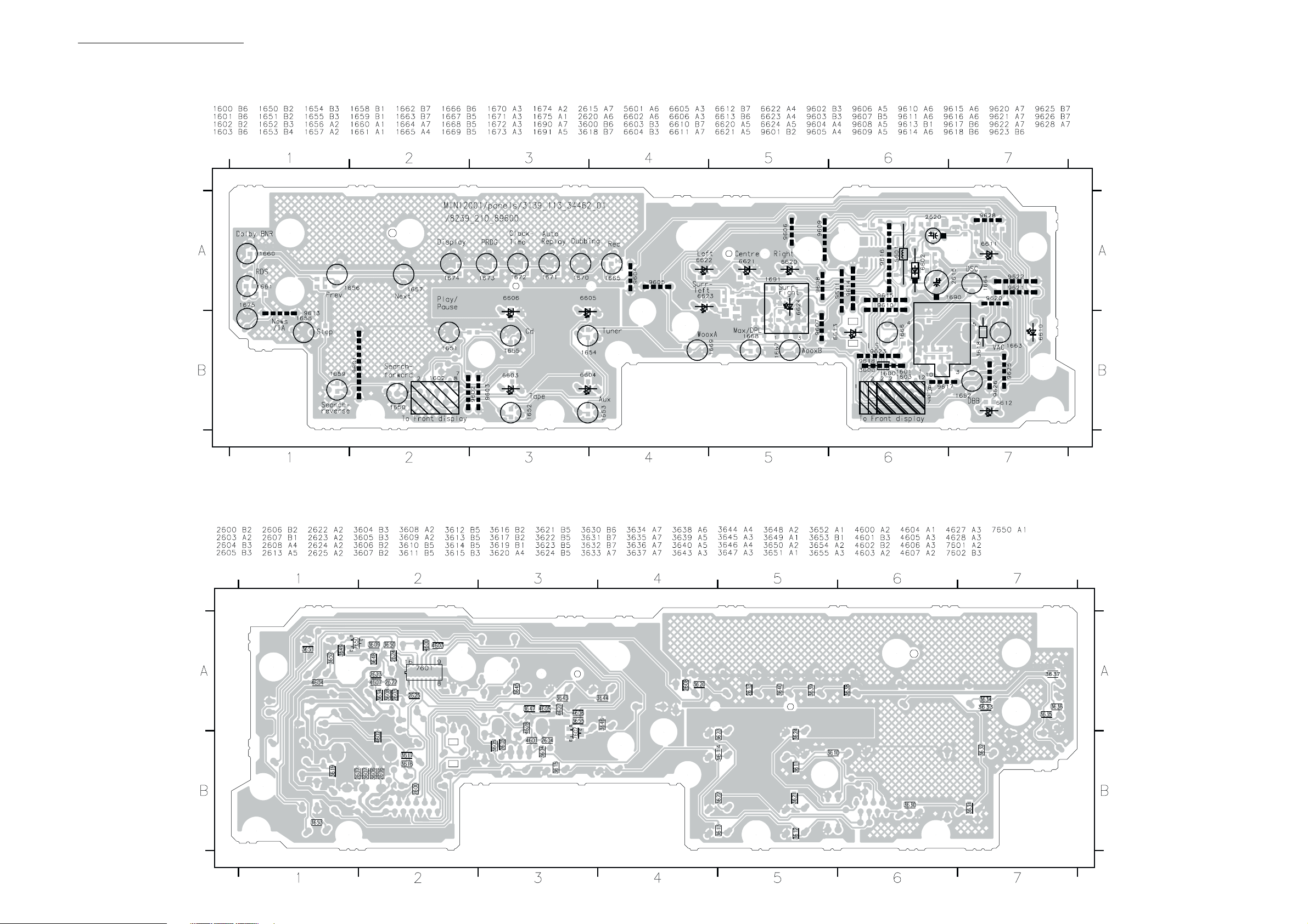
1600 F1
1601 H2
1602 D1
1603 H1
1650 D2
1651 C2
1652 C3
1653 C3
1654 C3
1655 C2
1656 D3
1657 D3
1658 D3
1659 D2
1661 D4
1662 C5
1663 C6
1664 C6
1665 C7
1666 C5
1668 C4
1669 C4
1670 C6
1671 D6
1672 D6
1673 D5
1674 D5
1675 D4
1690 B1
1691 A3
2600 G5
2603 G5
2604 B4
1667 C4
1660 D5
1234567
A
JOG_A
JOG_B
1690
EC16
MT14MT2
10K
3606
3607
1
2
3
5
2606
10n
2607
B
3610
150R
1651
GND-B
1650
GND-B
Gnd
Woox_A
Woox_B
Vac
DSC
9618
# 3600
470R
Max_Woox_LedShClk
+5V6
Gnd
Gnd
PLAY
3630
150R
S_fwd
Gnd
9610
Gnd Gnd
C
FE-ST-VK-N
D
E
F
G
1602
1600
FE-ST-VK-N
1
2
3
4
5
6
7
8
9
10
11
12
FE-ST-VK-N
1
2
3
4
5
6
7
8
1603
Key2
Key1
1
2
3
4
5
6
7
8
9
10
1601
FE-ST-VK-N
Tuner
Tape
1
2
3
4
5
6
7
8
GND-B
JOG_A
H
2605 B4
2623 F7
2606 B2
2607 B2
2608 C7
2613 D6
2615 A4
2620 F3
10K
10n
3611
220R
1652
1655
CD
GND-B
GND-B
3631
220R
1659
S_back
GND-B
GND-B GND-B
DBB_ShStr
IS_ShData
4600
VacJOG_B
6610
DSC
6611
6612
DBB_Led
IS_Led
6613
2624 G4
2625 G4
3600 G2
3604 A4
3605 A4
3612
270R
TAPE
3632
270R
1658
+5V6
2620
3649
3648
Gnd
Green-Led
10u
10K
3607 A2
3608 G5
3609 G4
3610 C2
3611 C3
3612 C3
Woox_A
Woox_B
3613
390R
1653
AUX
GND-B
3633
390R
1657
STOP
GND-B GND-B
Tap eCD
Aux
TunerAux
CD
7650
BC847B
10K
3654 120R
1691
EC12
MT14MT2
Gnd
GND-B
NEXT
220R3651
220R3652
270R3653
1654
3650
Gnd
+5V6
3613 C3
3614 C4
3615 C4
3616 C5
3617 C5
3618 C6
3619 C6
5
3614
560R
1656
4K7
1
TUNER
3621
120R
3622
120R
3623
120R
3624
120R
3
2
1669
GND-B
3634
560R
PREV
10K
Gnd
3620 C7
3621 E4
3622 E4
3623 E4
3624 E4
3630 D2
3631 D3
1675
GND-B
Tape
Aux
Tuner
CD
220p
3609
Gnd
3604
2604
Gnd
WOOX_A
GND-B
3635
820R
2624
10n
1668
NEWS
6603
6604
6605
6606
Max_Woox_LedShClk
3606 A2
2622 F6
+5V6
6602
10K
3605
2605
Gnd
3615
820R
DBB_ShStr
IS_ShData
3632 D3
3633 D3
3634 D4
3635 D4
3636 D4
3637 D5
3638 D5
1N4148
10K
10n
Max/DPL
3636
1K2
1661
Green-Led
Gnd
220p
Gnd
2615
Gnd
1667
GND-B
RDS
2625
3639 D6
3640 D6
3643 G6
3644 G6
3645 G6
3646 H7
3647 H6
47u
1660
GND-B
5601
220p
Gnd
WOOX_B
GND-B
3637
1K8
2u2
2600
3616
1662
Dolby NR
GND-B
10K
Gnd
4605
1K2
1674
3648 G3
3649 F3
3650 F3
3651 H3
3652 H3
3653 H3
3654 H3
DBB
3608
6604 E4
3655 H6
4600 G2
4605 H5
4606 H6
5601 F5
6602 A4
6603 E4
Note : Some values may varies, see respective
6620 G7
6605 E4
6621 G7
6606 E4
6622 G7
6610 H3
6623 H7
6611 H3
6624 H7
6612 H3
7601 F5
7602 H7
6613 H3
parts list for correct value.
# : Provision
3617
1K8
1666
IS
GND-B
3638
2K7
DISPLAY
GND-B
7601
74HC4094D
15
EN1
1
STB
3
2
D1
2603
220p
1673
SRG8
1664
GND-B
3639
4K7
16
8
PROG
Gnd
3618
2K7
DSC
GND-B
1672
1663
GND-B
4
5
6
7
14
13
12
11
9
10
3619
4K7
3640
4K7
CLK
GND-B
3643 180R
3644
4606
VAC
1671
1670
GND-B
180R
180R3645
3647
180R
3655
1K
AUTO REV
+5V6
2622
Gnd
Max_Led(Amber)
7650 F3
9610 G2
9618 G2
3620
10K
Dubbing
2613
GND-B
100n
6621
6622
6620
6624
Dpl_surr_R
1665
GND-B
100p
2623
Gnd
Gnd
REC
100n
7602
BC847B
Dpl_surr_C
Dpl_left
Dpl_right
DBB_Led
Gnd
Dpl_surr_L
6623
2608
GND-B
Vac
DSC
+5V6
100p
3646180R
This assembly drawing shows a summary of all possible versions.
For components used in a specific version see schematic diagram and respective parts list.
A
3139 113 3446 pt2 dd wk0116
B
IR-EYE BOARD - CIRCUIT DIAGRAM
C
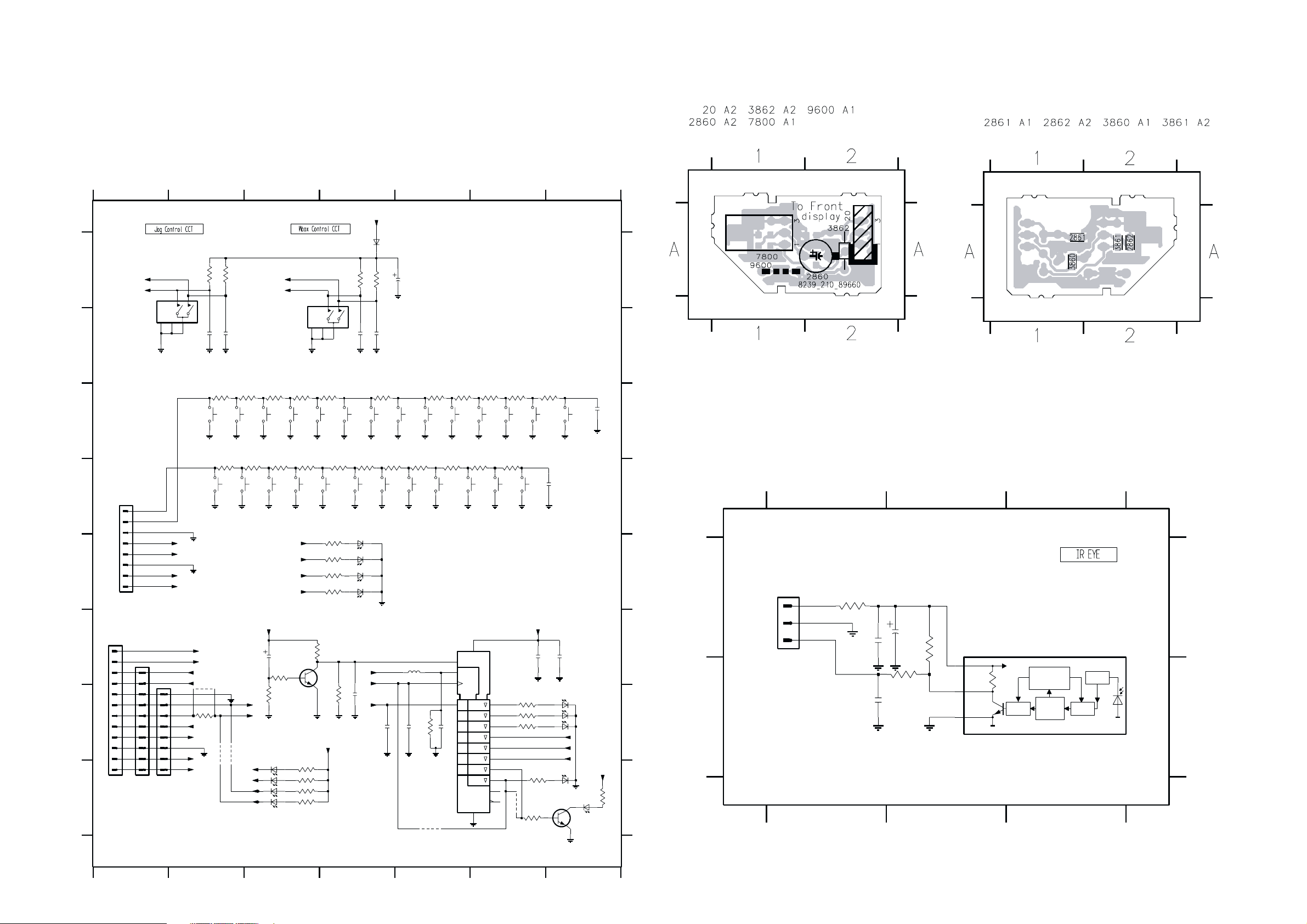
20 A1 2860 A2 2861 B1 2862 A1 3860 A1 3861 A2 3862 B2 7800 A2
D
123
Note : Some values may varies, see respective parts list for correct value.
E
20
Gnd
100R
3860
Gnd
47n2n2
2862
Gnd
3862
2861
Gnd
1K
47u
2860
Gnd
10K
7800
TSOP2236
3861
VS2
OUT1
DEM
CTRL
CIRCUIT
BAND
PASS
INP
AGC
GND3
3139 118 54530...for 89660...3446 pt2 dd wk0116
PIN
A
B
A
1
2
3
F
DIPMATE
G
B
H
123
3139 118 54530...for 89600...3446 pt2 dd wk0116
1234567
KEY-CDC BOARD - CIRCUIT DIAGRAMKEY-CDC BOARD - COMPONENT LAYOUT
This assembly drawing shows a summary of all possible versions. For components used in a specific version see schematic diagram and respective parts list.
KEY-CDC BOARD - CHIP LAYOUT
3139 113 3446 pt2 dd wk0116
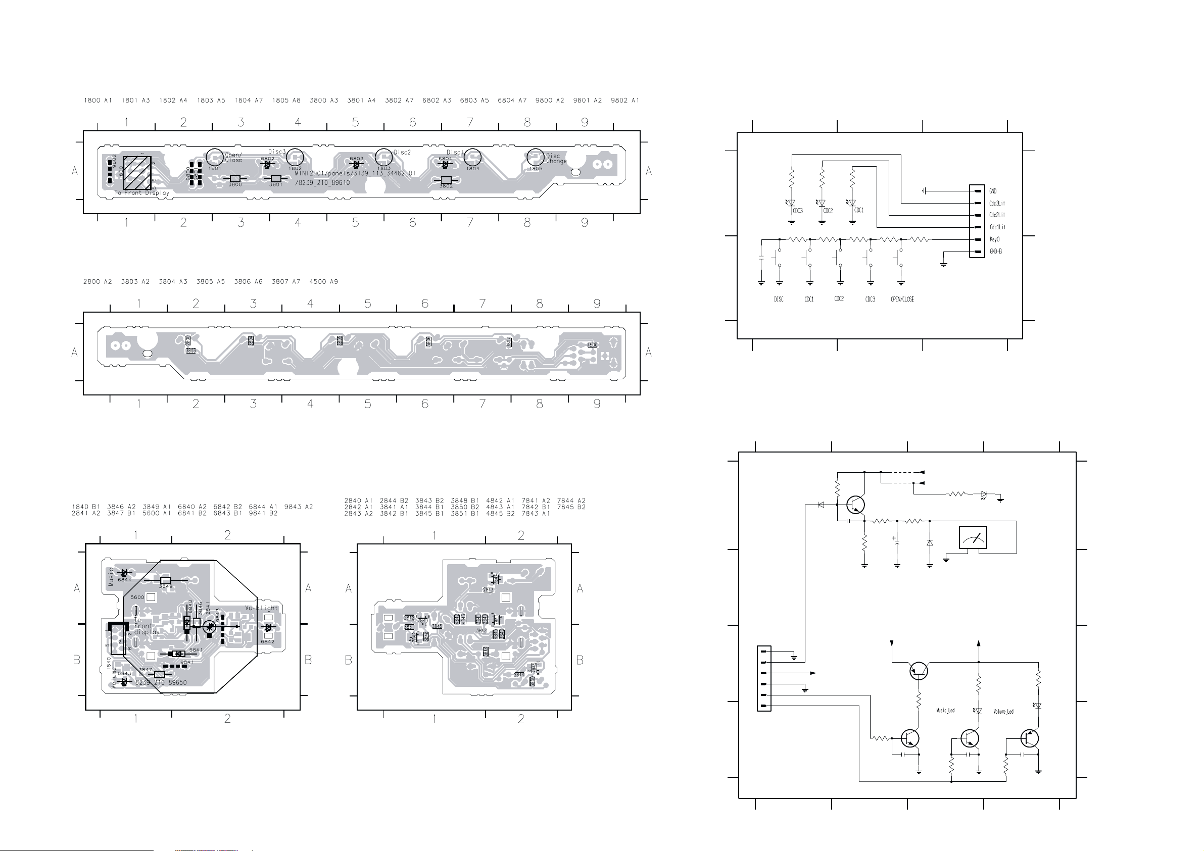
1800 A3
1801 B2
1802 B2
1803 B2
1804 B1
1805 B1
2800 B1
3800 A1
3801 A1
3802 A2
123
Note : Some values may varies, see respective parts list for correct value.
3801
3800
220R
220R
3802
220R
A
6804
3803
560R
1805
6803
1804
3804
390R
3805
270R
1803
3806
220R
1802
2800
6802
100p
B
GND-B GND-B
GND-B GND-B
1
GND-B
GND-B
3139 118 54530...for 89610...3446 pt2 dd wk0116
23
3803 A1
3804 A1
GND
3807
150R
1801
3805 A2
3806 A2
GND-B
3807 A2
6802 A1
FE-ST-VK-N
1800
1
2
3
4
5
6
6803 A1
6804 A2
A
B
This assembly drawing shows a summary of all possible versions. For components used in a specific version see schematic diagram and respective parts list.
VU METER BOARD - COMPONENT LAYOUT VU METER BOARD - CHIP LAYOUT
This assembly drawing shows a summary of all possible versions.
For components used in a specific version see schematic diagram and respective parts list.
3139 113 3446 pt2 dd wk0116
This assembly drawing shows a summary of all possible versions.
For components used in a specific version see schematic diagram and respective parts list.
3139 113 3446 pt2 dd wk0116
3139 113 3446 pt2 dd wk0116
VU METER BOARD - CIRCUIT DIAGRAM
1840 C1
2842 D2
3841 A2
3844 A3
3847 D4
3850 C4
2840 A2
2843 D3
3842 A2
3845 D2
2841 A2
2844 D4
3843 A2
3846 D3
3848 C3
3849 C3
1234
Note : Some values may varies, see respective parts list for correct value.
# : Provision
47K
3841
A
6840
1N4148
2840
100p
3842
7841
BC847B
3843
100K
B
1840
FE-BT-VK-N
1
C
2
3
4
5
6
To Front
D
VUMeter
+5V6
Gnd
Bit0
Bit1
3845
1K2
1K
+5V6
3851 A3
4842 A2
# 4842
4843
2841
2842
100p
3844
8K2
1u
BC857B
Gnd
4843 A2
5600 A4
6840 A1
+5V6
+Vu
6841
7842
3848
470R
7843
BC847B
1N4148
6841 A3
6842 A4
6843 D4
Vu-backlight
3851
180R
12
2843
100p
4K7
Gnd
3846
+Vu
6844
6844 D3
7841 A2
7842 C3
LB3333
6842
3849
150R
7844
BC847B
7843 D3
7844 D3
7845 D4
Gnd
5600
Vu-meter
3847
2844
100p
220R
Gnd
3850
6843
390R
BC857B
7845
A
B
C
D
3139 118 54530...for 89650...3446 pt2 dd wk0116
1234
KARAOKE BOARD - COMPONENT LAYOUT KARAOKE BOARD - CHIP LAYOUT
This assembly drawing shows a summary of all possible versions.
For components used in a specific version see schematic diagram and respective parts list.
3139 113 3446 pt2 dd wk0116
KARAOKE BOARD - CIRCUIT DIAGRAM
1700 C1
2700 C1
2703 C3
2706 A3
2719 C3
1701 A4
2701 C2
2702 C2
2704 C3
2705 B4
1702 D4
123 4
Note : Some values may varies, see respective parts list for correct value.
# : Provision
A
2720 B2
2707 E2
3700 B1
2708 E3
SIMPLE KARAOKE
(FOR /21 VERSION ONLY)
3701 C2
3702 C1
3703 C2
3704 C2
3705 B2
3706 C2
This assembly drawing shows a summary of all possible versions.
For components used in a specific version see schematic diagram and respective parts list.
3139 113 3446 pt2 dd wk0116
3707 C3
3711 B4
3714 E3
5700 C1
6701 E4
3709 B4
3710 C4
mic_gnd
3712 C4
3713 A4
agnd
2706
100u
5702
2u2
9702
3715 E3
4708 C3
agnd
5702 A4
6700 E3
3713
470R
7700 C2
7701 C4
1701
FE-BT-VK-N
4
+12A
3
MIC
2
agnd
1
MIC_DET
7702 E2
7703 E2
9702 A4
A
B
3
2
1
C
TC38
1700
agnd
agnd
6
5
4
8
7
9
mic_gnd
D
E
3139 118 54530...for 89630...3446 pt2 dd wk0140
123 4
5700
22u
mic_gnd
3702
+12A
3700
10K
# 2720
100n
1K5
# 3701
330R
2700
mic_gnd
agnd
agnd
3703
10K
4n7
7702
BC847B
agnd
2701
100n
2K7
3705
2703
3704
2702
mic_gnd
BC847B
470n
1M
7700
BC550C
3
1n
7703
3706
2707
agnd
33R
100n
3707
3714
agnd
20K
1
agnd
1M
FOR VIDEO CD ONLY
2719
3715
150K
3711
B
680R
2705
3709
1u
1M
4708
470n
2704
2
6700
1N4148
10u
2708
agnd
agnd
680p
3710
1N4148
agnd
7701
BC550C
330R
agnd
6701
agnd
3712
agnd
100K
FE-BT-VK-N
1
2
3
4
5
1702
C
D
+Kara
VCD_IN1
agnd
VCD_IN2
MIC_DET
E
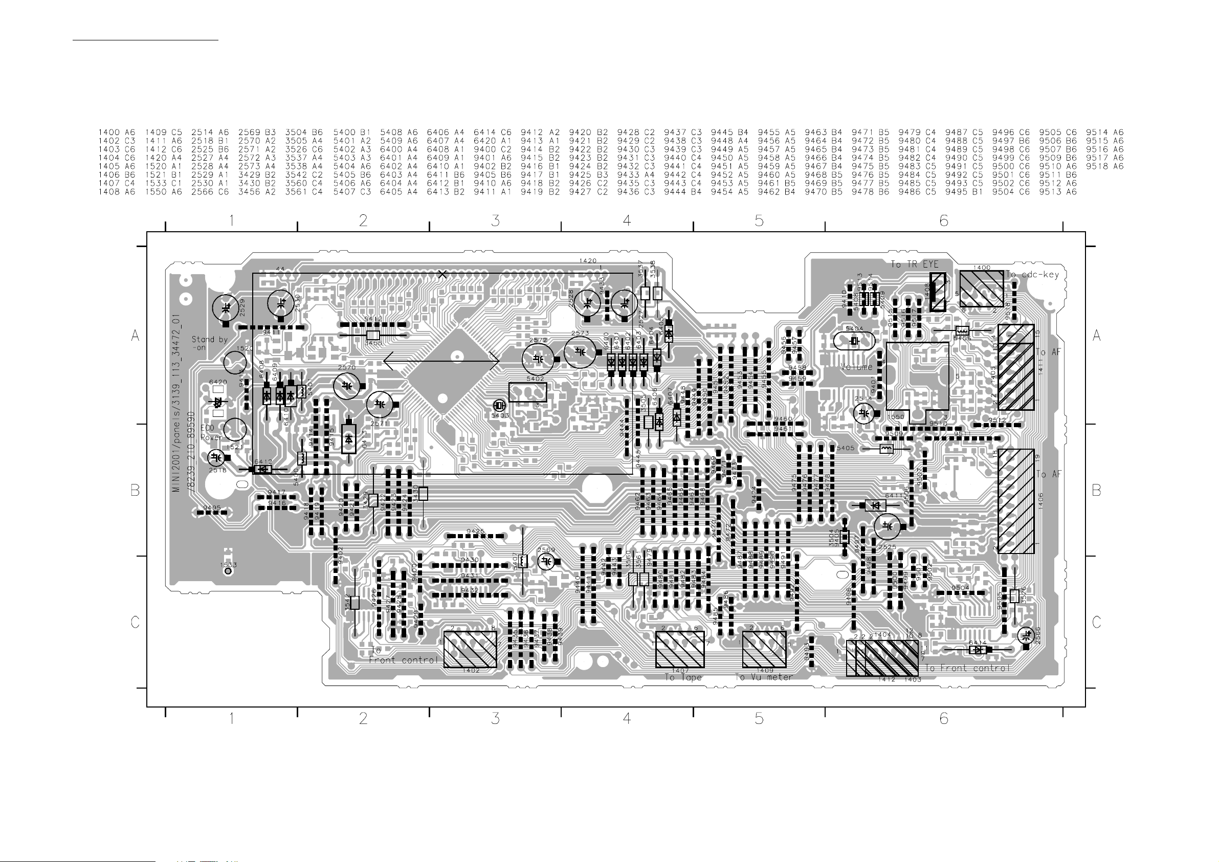
FRONT DISPLAY BOARD
FRONT DISPLAY BOARD - COMPONENT LAYOUT
This assembly drawing shows a summary of all possible versions. For components used in a specific version see schematic diagram and respective parts list.
3139 113 3447 pt2 dd wk0119

FRONT DISPLAY BOARD - CHIP LAYOUT
This assembly drawing shows a summary of all possible versions. For components used in a specific version see schematic diagram and respective parts list.
3139 113 3447 pt2 dd wk0119

FRONT DISPLAY BOARD - CIRCUIT DIAGRAM
1400 D1
1402 I18
1403 J20
1404 I20
1405 F20
1406 C20
1407 A20
1408 F1
1409 G1
1411 F20
1412 K20
1420 A10
1520 G7
1521 J9
1533 J16
1550 J16
2500 A3
2501 B4
2502 A4
2503 B5
2504 A6
2505 B6
2506 A7
2507 B7
2508 F8
2509 H17
2510 D5
2511 I1
2512 I1
2513 I1
2514 J1
2515 H3
2516 H4
2517 H5
2518 J8
2519 J10
2520 I10
2521 J10
2522 J10
2523 J12
2524 J12
2525 J12
2526 J13
2527 J14
2528 I14
2529 K14
2530 J14
2531 H14
2533 J15
2534 J17
2535 J17
2536 G15
2537 G15
2538 F16
2539 F16
2541 D14
2542 C15
2543 B16
2544 B17
2545 B19
2546 B19
2547 B19
2548 B19
2549 C19
2550 C19
2551 D19
2552 D19
2553 E19
2554 E19
2555 E19
2556 E19
2557 E19
2558 G18
2559 G19
2560 G19
2561 G19
2562 F19
2563 G20
2564 H7
2565 G4
2566 H7
2567 H9
2568 G10
2569 E16
2570 C13
2571 C14
2572 F9
2573 F9
2574 G11
2575 G11
2576 G11
2577 H10
2578 C13
2579 B9
2580 B9
2581 B13
2582 B13
2583 A18
2584 A18
2585 G7
2586 G7
2587 I10
2588 C19
2589 I13
3400 F9
3401 F10
3402 F10
3403 F10
3404 F10
3406 H16
3407 I14
3408 I14
3409 G10
3410 J14
3411 J14
3413 F9
3414 F11
3415 F11
3416 F12
3417 F12
3418 F12
3419 F12
3420 F12
3421 F12
3422 F12
3423 F13
3424 F13
3425 F13
3428 E13
3429 E13
3430 E13
3431 E13
3432 E13
3433 D13
3434 D13
3435 D13
3436 D13
3437 D13
3438 F18
3439 F18
3444 C13
3445 C12
3446 C12
3447 C12
3448 C12
3449 C12
3450 C12
3451 C11
3452 C11
3453 C11
3454 C11
3455 C11
3456 C11
3457 C11
3458 C10
3459 C10
3460 C10
3461 C10
3462 C10
3463 C10
3464 C10
3465 C9
3466 D9
3467 D9
3468 D9
3469 D9
3470 D9
3471 D9
3472 D9
3473 E9
3474 E9
3475 E9
3476 E9
3477 E9
3479 E9
3480 F9
3485 J7
3490 D20
3491 E20
3492 E20
3500 B4
3501 B5
3502 B6
3503 B7
3504 E8
3505 E8
3511 D7
3512 E7
3515 H3
3516 H3
3517 I5
3518 J5
3519 J5
3520 J5
3521 H7
3522 H7
3523 H8
3526 H7
3527 I8
3528 I9
3529 I11
3530 J11
3531 H13
3532 H14
3533 H13
3534 H13
3535 I14
3536 J14
3537 I14
3538 J14
3539 I15
3540 I17
3541 I17
3542 G16
3543 H16
3544 H16
3545 H16
3546 H16
3547 G16
3548 G16
3549 G16
3550 E16
3551 E16
3552 E16
3553 D15
3554 D14
3555 D16
3556 D16
3557 C16
3558 C16
3559 C16
3560 A18
3561 A18
3562 A19
3563 F18
3564 C19
3565 C20
3570 I14
3571 J14
3572 B20
3573 E5
3574 F8
3575 G6
3576 F18
3577 F19
3578 F19
3579 F19
3580 F20
3581 G20
3582 G20
3583 G19
3584 G20
3585 H19
3586 H18
3587 H19
3588 I19
3589 I10
3590 J10
3591 J10
3592 E7
3593 E7
3594 E7
3595 D7
3596 D7
3597 F18
3598 F5
3599 G4
4401 D18
4430 K20
5400 G13
5401 C14
5402 F11
5403 F11
5404 H3
5405 H4
5406 G19
5407 F15
5408 E1
5409 F1
6400 E8
6401 E8
6402 E8
6403 E8
6404 E8
6405 I16
6406 I10
6407 F1
6408 I12
6409 C14
6410 B14
6411 I12
6412 I8
6413 C14
6414 H8
6415 F10
6420 J8
7400 C9
7401 H1
7402 D5
7403 B15
7404 F15
7405 H12
7406 G11
7407 J10
7408 B5
7409 B7
7410 B6
7411 J8
7412 B4
7413 E15
9400 K19
9405 E8
9513 F1
9514 F1
1 2 3 4 5 6 7 8 9 1011121314 1516171819 20
470R
470R
470R
2572
LPSKey
2579
220p
470R
470R
470R
470R3471
470R
470R
470R3476
470R
470R
47u
PWRDWN
1420
2581
220p
33031323334353637424344 7891314171819 220212223242526272829
1101112
220p
G11
3446
P1
470R
7405
M24C02
E0
E1
E2
SCL
WC_
G13
G12
3445
470R
470R
V4
V3
80k pull down
3-B. I/O P3
( tristate )
INT2
TC1
470R
3420
3421
2525
100n
2523
3444
INT4
470R
3422
+5V6
5400
+5V6
8
VCC
SDA
VSS
2589
1u
47u
100n
2524
100n
2582
414243444546474849550515253
V0V1V2
VDD
VAREF
VASS
AIN13
P5
AIN12
AIN11
AIN10
4-Bit In/Output
(tri-state)
AIN7
P4
AIN6
AIN5
AIN4
AIN3
AIN2
8-Bit Input/Output
(tri-state)
AIN1
AIN0
-SCKO
SCA
SCL
470R
470R
3423
3424
2u2
5
4
+F
+D
2526
220p
2580
3461
3460
470R
470R
V19
V20
8-Bit h. break. v.
down
drain 80k p.d.
P0
P05
P06
470R
470R
3404
3403
33p
2577
+5V6_Con
2587
1K
100K
3590
470R
V18
P07
1u
2521
6415
47K
3409
3459
7
BAS316
2568
"ON"0.7V
10n
P1P2P3P4P5P6P7
G3G2G1
G4
3454
3458
470R
470R
V16
V17
VFT driver circuit (automatic display)
3453
3456
3455
3457
470R
470R
470R
470R
54555657585966061626364
V12
V13
V14
V15
8-Bit high breakdown voltage 8-Bit high breakdown v.
output port with latch output port with latchout w. latch P8
ROMRAM
G9G8G7G6G5
3450
3449
3451
3448
3452
470R
470R
470R
470R
470R
V11
V10
P7 P6
80k pull down80k pull down
P6-P9 source open drain
Program
Counter
CPU
drain
sink o.
XIN
XOUT
VSS
-RESET
XTOUT
8809
10 11 12 13 14 15 16 17 18 19220 21 22 23 24
5402
2p2
22p
2576
0.3V"ON"
7406
BC847B
Options
6406
1N4148
2522
100n
3591
100K
8-Bit I/O P2
sink o.drain
XTIN
5403
32K768
22p
2575
TEST
2574
RESET
3529
3530
-STOP
470R
3414
3415
22p
+C
2K7
1K8
8-Bit Input/Output
(tri state)
TC2
-INT0
-INT1
470R
470R
3416
3417
+5V6
+5V6 +5V6
G10
3447
470R
470R
V5V6V7V8V9
8-Bit A/D
Converter
TC4
-DV0
T
470R
470R
3418
3419
1
2
3
6
7
6408
1N4148
6411
1N4003
Items
3407 , 3408 , 3410 , 3411
3535 , 3536 , 3570 , 3571
Items
3479 , 3480 , 3422
P8
3464
3463
3462
470R
470R
470R
7400
65
V21
V23
V22
V24
66
V25
67
V26
68
V27
80k pull
69
V28
70
V29
71
V30
72
V31
8-Bit h. breakdown v.
out. port w. latch P9
73
V32
PD
74
V33
source open
75
V34
76
V35
77
V36
5-Bit h. breakd. v.
out w. latch
VKK
78
8-Bit Input/Output
-SCK1
79
(tri-state)
SI1
P03
P04
SO1
1
4
3
3400
470R
470R
470R
3401
3402
RESET
10n
3589
2520
10n
2519
7407
BC847B
Note : Some values may varies, see respective parts list for correct value.
@ : For DPL only
: For RDS only
*
# : Provision
7403
74HC4094D
SRG8
15
220p
-Vkk1
7413
BC847B
7404
74HC4094D
15
1
3
2
3539
2533
100n
EN1
1
STB
3
2
D1
4K7
3550
16
SRG8
EN1
STB
D1
8
BZX79-B4V7
6405
22K
GND-B
1533
-F1
2578
100n
2570
40
39
38
3437
37
470R
3436
36
470R
3435
35
470R
3434
34
470R
3433
33
470R
3432
32
31
3431
3430
30
3429
29
3428
28
27
26
3425
25
470R
3531
3533
1K
3534
1K
3570
F1
3535 10R
3407
3408
10R
3571
F2
3536
3410 10R
3411
10R
For 30-70W Set
4R7
VCD
100R 470R
470R
470R
470R
470R
470R
470R
10K
6410
10K
2527
1N4003
1N4148
1N4003
2531
I2C_DATA
47u
47u
2529
6409
6413
LowPwrCtr
LEDShEn
LEDShDATA
LEDShSTR
LEDShCLK
1u
I2C_CLK
47u
47u
2528
-Vkk1
2530
-Vkk1
+5V6
+5V6_Con
+5V6
3554
2541
220p
120R
120R
220p
2542
10K
10K
3553
5407
2u2
2537
2536
220p
-F1
3537
-F2
3538
+L
5401
2u2
47u
+C
47u
2571
3532
10R
10R
10R
10R
Others
10R
Non-VCD
3490
470R
3491 470R
3492
470R
3580
3581
35821K
256310n
3584
1K
LowPwrCtr
FE-ST-VK-N
FE-ST-VK-N
1403
1
2
3
4
5
6
7
8
1
2
3
4
5
6
7
8
9
10
FE-ST-VK-N
1407
1
2
3
4
5
6
7
FE-ST-VK-N
1406
1
2
3
4
5
6
7
8
9
10
11
12
13
14
15
16
17
18
19
1411
FE-ST-VK-N
1
2
3
4
5
6
7
8
9
10
11
12
1412
FE-ST-VK-N
FE-ST-VK-N
1405
1
2
3
4
5
6
7
8
9
10
11
12
13
14
15
1404
A
B
C
D
E
F
1
2
3
4
G
5
6
7
8
9
10
11
H
I
J
K
100p
2583
100p
2584
3560100R
TpADC2
3561 100R
TpADC1
+C
DBB_ShStr
IS_ShData
Max_Woox_ShClk
TU_Enab
MuxEnable
+D+D
10K
10K
3541
10n
10n
2535
TPShCLK
TPShDATA
TPShSTR
220n
2545
AmNTC
Cdc1
Cdc2
I2C_DATA
Cdc3
I2C_CLK
Vac
DSC
+5V6_Con
Tu_RDS_Out
TuStereo
Tu_Clk
Tu_Data
Tu_Enab
Bit0
Bit1
CD
HP_DET
Tuner
SA
Aux
PWRDWN
Tape
Clipping
MicDetect
IoVolClk
LEDShClk
LEDShData
FE-ST-VK-N
1402
+5V6
# 3597
2588
220n
+12V_D
4401
2K2
2K2
3439
3438
+D
10K
10K
10K
3563
3576
3577
100p
100p
100p
2559
2558
3585
3586
330K
1K
1K
@ 3587
1K
@ 3588
1
Key2
2
Key1
3
4
CD
5
Tuner
6
7
Aux
8
Tape
+5V6
16
100n
2543
2544
100n
"ON"
0
5V
4
5
6
3559 220R
7
220R3558
14
220R3557
13
3556 220R
12
220R3555
11
9
10
8
+5V6
10u
2569
10K
3551
10K
3552
+5V6
100n
2539
2538
100n
3549 220R
4
220R3548
5
3542 220R
6
120R3547
7
3546 120R
14
120R3545
13
3544 120R
12
220R3543
11
9
@ 3406
10
470R
100p
IS_ShData
@ 2509
VOL_A
1550
EC16
MT14MT2
VOL_B
5
12
3
3540
2534
-Vkk
VOL RE
10K
3562
2K2
220p
2547
2546
220p
220p
2548
3572
3564
220R
254910p
3565
220R
10p2550
-Vkk
F1
F2
10p2554
10p2556
10K
2560
3578
100p
2553 47p
10K
2561
2552 47p
10p2557
10K
3579
3583
22K
5406
2u2
WooxA
WooxB
Vac
DBB_ShStr
IS_ShData
Max_Woox_ShClk
JOG_A
JOG_B
LEDShClk
LEDShSTR
47p2551
100n2555
2562
@ 9400
1n
1K
1K
+5V
@ 4430
6
3139 118 54300...for 89590...3447 pt2 dd wk0138
13 14 15 16 17 18 19 20
Model (Mini 2001)
FW-C550/37
A
B
FW-C700/37
FW-C700/34
FW-C700/22
FW-C720/21
FW-P750/37
FW-C780/21/22/30/37
FW-C780/34
FW-C780/33
Model (Mini 2002)
FW-C700/21
FW-C785/22
FW-C785/34
C
FW-C788/21/21M
FW-C788/33 12K
FW-V520/21M
FW-C798/21/37
FE-ST-VK-N
D
1400
1
2
3
4
5
6
E
1408
1
2
1409
FE-ST-VK-N
EH-B
3
1
2
3
4
5
6
F
G
H
47p
2512
2511
560p
*
I
J
*
560p
2513
*
2514
*
Option_R Ohms (3530)
180RFW-C500/37
470R
820R
1K2
1K8
820R
2K7
3K9FW-P750/22/34
5K6
8K2
12K
Option_R Ohms (3530)
470RFW-C555/21/37
820R
5K6
8K2
5K6
5K6FW-C788/30/37
5K6
27KFW-V780/21M
5K6
Cdc3
Cdc2
Cdc1
Key0
+5V6_Con
5408
2u2
6407
9513
1N4148
9514
2u2
5409
+5V6
VUMeter
RC5
Bit0
Bit1
*
7401
*
SAA6579T
57 Khz
ANTI-
4
MUX
ALIASING
FILTER
8
SCOUT
CLOCKED
7
CIN
COMPARATOR
5
VDDA
VP1
REFERENCE
3
VREF
VOLTAGE
2u2
VSSA VSSD
6
BANDPASS
(8th ORDER)
COSTAS LOOP
VARIABLE AND
FIXED DIVIDER
CLOCK
REGENERATION
AND SYNC
RECONSTRUCTION
FILTER
TEST LOGIC AND OUTPUT
+F +F +F +F
2500
100p
G1
AT-51
5404
*
82p
2515
3516
*
3515
*
220K
13
14
OSCI
OSCO
OSCILLATOR
AND
DIVIDER
BIPHASE
SYMBOL
DECODER
SELECTOR SWITCH
MODE
9
TEST
2K2
*
10
7412
BC847B
82K
3500
2501
+D
2u2
47p
5405
2516
*
+5V
12
VDDD
QUALITY
BIT
GENERATOR
DIFFERENTIAL
DECODER
11
100p
G1’
LEDShClk
LEDShData
QUAL
RDDA
RDCL
100p
2502
7408
BC847B
82K
3501
-Vkk-Vkk
G11
7402
HEF4051BT
11
A0
10K
3573
A1
10
A2
9
10K
3598
3599
6
E_
470R
47p
2565
2517
100n
*
1
3517
2
*
10K
3518
16
*
10K
15
T57
10K
3519
2503
100p
G11’
+D
16
VDD
LOGIC
LEVEL
CONVERSION
VSS
8
TuRDSData
TuRDSClk
10K
3520
2510
100n
2504
100p
G12
1-of-8
DECODER
7410
BC847B
82K
3502
-Vkk
VEE
7
GND-B
2506
100p
7409
BC847B
82K
2505
100p
G12’
3512
13
Y0
1K
3592
14
Y1
1K
3593
15
Y2
1K
3594
12
Y3
1K
1
Y4
5
Y5
2
Y6
4
Y7
Z
3
10K
220p
# 3575
3503
100p
2507
-Vkk
2K7
2564
Key0
Key1
Key2
HP_DET
AmNTC
MicDetect
2566
G13’
2K7
3596
IoVolClk
470R
3505
470R
3504
6414
1N4148
6
2518
-Vkk
10K
3574
3523
470K
+L
4u7
3527
820R
BC857B
7411
6420
# 9405
2586
+C
3521
680K
1u
47K
3522
+5V
6412
1N4148
47K
3485
G13
+C+C +C
2K7
3595
3511
1520
220p
2585
3526
15K
1n
P11
1N41486404
6403 1N4148
1N41486402
6401 1N4148
1N41486400
47n
2573
# 2508
2567
220n
P10
47u
3413
+L
3528
-F2
P9
TMP88CU74YF
3465
3466
3467
3468
3469
3470
3472
3473 470R
3474
3475 470R
3477 470R
3479
3480
1M
10K
1521
K
12
3456789101112

TAPE ADJUSTMENT & CHECK TABLE
HEADPHONE BOARD - COMPONENT
LAYOUT
This assembly drawing shows a summary of all possible versions.
For components used in a specific version see schematic diagram and respective parts list.
3139 113 3447 pt2 dd wk0119
HEADPHONE BOARD - CIRCUIT DIAGRAM
1850 C1
1851 B3
1890 A3
1891 C3
1892 C3
2850 A2
2851 A3
2852 A2
123
Note : Some values may varies, see respective parts list for correct value.
# : Provision
## : Provision for ESD
HEADPHONE BOARD - CHIP LAYOUT
This assembly drawing shows a summary of all possible versions.
For components used in a specific version see schematic diagram and respective parts list.
3139 113 3447 pt2 dd wk0119
2853 A2
2854 C3
5850 B1
5851 A2
# 9550
5852 B2
9550 A2
TEST
CASSETTE
RECORDER
MODE
MEASURE
ON
ADJUST MOTOR SPEED
NORMAL SPEED
SBC420
3150Hz
PLAY B
PLAY A
1
LEFT
or
RIGHT
CHECK WOW & FLUTTER
DECK A & B
SBC420
3150Hz
PLAY
1
LEFT
or
RIGHT
ADJUST AZIMUTH
PLAY FWD
PLAY REV #
1
LEFT
or
RIGHT
DECK A & B
SBC420
10kHz
CHECK PLAYBACK FREQUENCY RESPONSE
or
DECK A & B
SBC420
PLAY
1
LEFT
RIGHT
ADJUST BIAS CURRENT
DECK B
SBC419A^
RECORD
SBC420
5
LEFT
or
RIGHT
CHECK OVERALL FREQUENCY RESPONSE AND DISTORTION
Inject 3mV signals
100Hz, 250Hz, 1kHz,
10kHz, 12.5kHz
via
or
3
4
SBC419A^
or
SBC420
RECORD B
2
2
2
2
6
READ ON
frequency
counter
W&F-meter
mV-meter
mV-meter
mV-meter
ADJUST
with
3620
check
check
left hand screw
right hand screw
check
3773
check
to
3150Hz +/- 0.5%
3150Hz -0.8/+1.8%
<0.4 % DIN
max. output level
& left=right
limits see fig.1
995mV
750mV +/- 1.5dB
A
B
C
HP_DET
HP_RIGHT
HP_GND
HP_LEFT
5851
2u2
2853
100n
9
7
8
4
5
6
HP
##1891
RT-01T
2851
22n
HP
1
2
3
##2854
1
3139 118 54300...for 89620...3447 pt2 dd wk0119
470n
1851
TC38
1890
##1892
RT-01T
1
RT-01T1
TO AF9
1850
1
2
3
4
FE-BT-VK-N
5850
HP
2u2
5852
2850
22n
2852
22n
2u2
123
A
B
C
RECORDED
CASSETTE
Inject 1kHz 8.85mV
via
or
3
4
SBC419A^
SBC420
RECORDED
CASSETTE
SBC419A^ : 4822 397 30069
SBC420 : 4822 397 30071
level(dB)
8dB
80
or
250
6dB
figure. 1
PLAY B
RECORD B
PLAY B
4k
or
RIGHT
or
RIGHT
2
2
mV-meter
THD-meter
check
check
limits see fig. 2 *
<3% *
1
LEFT
1
LEFT
# For Auto-reverse version only
* If high frequencies are not within limits, decrease bias and re-measure.
If distortion is too high, increase bias and re-meaure
^ Not applicable for Ferro version
level(dB)
8dB
12.5k
f(Hz)
8dB
10dB (HSD)
100
250
6dB
figure. 2
4k
8dB
10dB (HSD)
f(Hz)
10k

AF9 BOARD
AF9 BOARD - COMPONENT LAYOUT
This assembly drawing shows a summary of all possible versions. For components used in a specific version see schematic diagram and respective parts list.
3139 113 3435 pt4 dd wk0123

AF9 BOARD - CHIP LAYOUT
This assembly drawing shows a summary of all possible versions. For components used in a specific version see schematic diagram and respective parts list.
3139 113 3435 pt4 dd wk0123

AF9 BOARD - CIRCUIT DIAGRAM (PART 1)
1 234567891011121314
1K5
3507
10K
3508
10K
1u
P
GND_A
SS_R
SS_L
3712
3511
820R
3512
820R
3532
A_Tp
P
2503
0V
100K
A_CD
A_CD
3533
27K
3534
27K
1K5
3437
A_Tp
1u
3667
1M
7663
BC857B
5.4V
3521
1K
3522
1K
3513
3514
3436
1K
P
4K7
A_Aux
#
FE-BT-VK-N
# only for
SOLID STATE
3661
2K7
P
5.6V
3668
10K
3669
3662
4K7
2K7
A_TU
3K3
3K3
P
A_TU
P
A_Tp
2535
2536
3438
1
2
3
4
5
3523
3524
4u7
4u7
1502
TU_Left
only for
CDR
1532
FE-BT-VK-N
1
2
3
A_Tp
4
5
6
7
A_Tp
-CMOS
3503
12K
100p
3504
12K
100p
+12V_A
MIC_DET
1V
470p
GND_A
1V
470p
GND_A
A_Mic
2663
1n
2664
1n
TU_Right
CD_Left
CD_Right
3505
A_Aux
3506
A_Aux
2661
1u
BC847B
7661
BC847B
7662
2662
1u
15K
15K
3531
A_Tp
3435
1K
#
#
2504
4.6V
3663
2K2
3664
2K2
4.6V
A
+12V_M
9618
P
2
1
2923
GND_EMC
1
2
3
4
5
6
7
5403
2u2
9654
P
5404
2u2
10n
+12V_A
GND_M
A_Tp
EH-B
1506
B
FE-BT-VK-N
1531
TP_REC_LEFT
C
TP_REC_RIGHT
GND_A_Tp
TP_LEFT
+12V_A
TP_RIGHT
-CMOS
D
3501
4K7
GND_EMC
4
E
4920
2669
2
100n
A_Aux
1
3
1501
YKC21-3418
AUX IN
F
MIC_DET
1510
FE-BT-VK-N
A_Aux
1
2
3
4
5
1503
FE-BT-VK-N
2501
A_Aux
3502
4K7
2502
A_Aux
1
2
3
4
G
GND_A
3665
470R
2665
GND_A
3666
470R
2666
GND_A
GND_A
100n
2667
2904
100n
4
2
H
1
3
1504
YKC21-3418
LINE OUT
I
1 234567891011121314
4K7
4K7
4K7
2513
A_CD
2514
A_CD
2531
2521
100n
2522
100n
1n
1n
SS_L
Line_L
Line_R
SS_R
2532
4u7
1
2
3
only for
Game Sound Port
LINE_L
-Vkk
+5V6
Mute2
LINE_R
4u7
2511
2512
1505
EH-B
1501 E1
3511 A3
1502 E3
3512 B3
1503 F1
3513 A3
1504 H1
3514 B3
1505 E4
3521 A3
1506 A1
3522 A3
1510 F1
3523 A3
1531 C1
3524 A3
1532 C2
2593
2591
330n
D
2203
GND_A
2516
5.9V
2206
GND_A
2507
100n
+IS
+9.1V
22n
47u
GND_A
100p
2506
GND_A
SUB_W
MUTE_SW_FR
3542
D
1K
3541
1K
100p
LINE_L
27
1
28
3
4
5
6
2
23
24
25
26
LINE_R
7501
TDA7468
POWER
SUPPLY
SOURCE
SELECTOR
47K
3543
0u47
2541
GND_A
S
3545
5K6
3549
18K for S
2543
10K for S
10n for S
3547
3K3
GND_A
8
7
VOLUME I
SUR.
SUR.
21
22
LEFT
LOGIC
VOLUME I
RIGHT
GND_A
3548
3K3
10K for S
2544
10n for S
3550
18K for S
S
3546
5K6
2542
0u47
47K
3544
GND_A
1u
DPL_R
3201
3202
2204
GND_A
BC847B
150R
9.8V
220u
7201
820R
6201
1N4148
9.1V
6202
GND_A
A_Mic
A_HP
A_TU
100u
2201
GND_A
22u
2202
GND_A
BZX55-C9V1
4.6V
VREF
A_DPL
1u
2205
11.7V
2n2
GND_A
A_Aux
A_Tp
A_CD
+12V_A
3525
470R
3526
470R
1n
GND_EMC
4501
2924
GND_A
P
4813
P
2921
100n
2698
100n
2505
GND_A
GND_A
100p
2515
1
2
3
YKC21-3416
1691
GND_A
100p
2533
GND_A
3700
GND_A
100p
GND_AGND_A
3K3
GND_A
2523
100p
3699
470R
0V
7693
BC817-25
100p
2524
GND_A
GND_A
2697
470p
GND_A
0V
3690
1K
SUBWOOFER
OUT
2534
2696
100p
GND_A
22u
DPL_L
5K6
33n
2565
4n7
2546
4n7
33n
5K6
SIMPLE I.S.
1n
2567
9
TREBLE
LEFT
TREBLE
RIGHT
20
1n
2568
SIMPLE I.S.
2590
2589
GND_A
GND_A
220n
2547
2548
220n
3n3
3n3
101911
BASS
BASS
RIGHT
GND_A
LEFT
3592
3591
GND_A
18
2592
330n
8K2
8K2
3593
GND_A
2549
470n
VOLUME II
LEFT
BASS ALC
IIC BUS
REC
VOLUME II
RIGHT
2550
470n
3594
GND_A
5K6
5K6
2594
470n
470n
3566
3568
GND_A
12
16
14
15
13
17
680K
220K
3551
5K6
3553
5K6
3552
5K6
3554
5K6
2554
2556
GND_A
3n3
470p
2551
1n8
2707
2552
1n8
GND_A
+IS
3645
220R
100p
3646
220R
+IS
3564
7586
BC847B
3570
3563
10K
3n3
3565
680K
3567
GND_A
220K
GND_A
2553
2555
470p
7585
BC847B
3569
GND_A
10K
2557
3571
100n
8K2
3555
8K2
1n
8K2
3557
2559
GND_A
GND_A
2708
ALC_LEVEL
P
3707
3708
100p
GND_A
3643
12K
1K
1K
2908
100n
I2C_Clk
I2C_Data
GND_D
P
6641
1N4148
P
6642
1N4148
2641
GND_A
2642
GND_A
1n
1n
3556
8K2
1n
8K2
3558
2560
10K
10K
2558
100n
GND_A
GND_A
3572
8K2
FULL I.S.
D...for DPL
S...for simple I.S.
P...provision
Note : Some values may varies, see respective parts list
for correct value.
FULL I.S.
+IS
1K
3561
3559
33K
2561
220p
7485
BC847B
GND_A
3641
220R
4641
4642
3642
220R
3560
33K
2562
220p
GND_A
3139 118 53770...88340 for...3435 pt4 dd wk0123
+IS
3562
7488
BC847B
470p
2563
GND_A
VOL_L
VOL_R
1K
2564
GND_A
470p
A
B
C
D
E
F
G
H
I
1691 H5
2201 B7
2202 C7
2203 D7
2204 C6
2205 C5
2206 C7
2501 E2
2502 E2
2503 D3
2504 E3
2505 F5
2506 F7
2507 E7
2511 A4
2512 B4
2513 A4
2514 B4
2515 F6
2516 F7
2521 A4
2522 A4
2523 F6
2524 F6
2531 D4
2532 C4
2533 F6
2534 F7
2535 B3
2536 C3
2541 A8
2542 H8
2543 C9
2544 G9
2546 F9
2547 B10
2548 G10
2549 C11
2550 F11
2551 C11
2552 F11
2553 B12
2554 G11
2555 B12
2556 H11
2557 B13
2558 G12
2559 C12
2560 G12
2561 C14
2562 G14
2563 C14
2564 G14
2565 C9
2567 B9
2568 G9
2589 A10
2590 I9
2591 A10
2592 I10
2593 A11
2594 I11
2641 D13
2642 E13
2661 G2
2662 I2
2663 H2
2664 I2
2665 H2
2666 H2
2667 G1
2669 E1
2696 G7
2697 H7
2698 G5
2707 E11
2708 E12
2904 G1
2908 E12
2921 G5
2923 B1
2924 F5
3201 B6
3202 C6
3435 D3
3436 D3
3437 D3
3438 D3
3501 D1
3502 E1
3503 D2
3504 E2
3505 E2
3506 E2
3507 E3
3508 E3
3525 E6
3526 E7
3531 C2
3532 C3
3533 B3
3534 C3
3541 A7
3542 I7
3543 A9
3544 I9
3545 B9
3546 G9
3547 C9
3548 F9
3549 B9
3550 G9
3551 C11
3552 F11
3553 C11
3554 F11
3555 C12
3556 F12
3557 C12
3558 G12
3559 C14
3560 F14
3561 B14
3562 F14
3563 A12
3564 G11
3565 B12
3566 G11
3567 B12
3568 H11
3569 B13
3570 H11
3571 B13
3572 G13
3591 A10
3592 I10
3593 A10
3594 I10
3641 D14
3642 E14
3643 D12
3645 D11
3646 E11
3661 G3
3662 I3
3663 G3
3664 H3
3665 G1
3666 H1
3667 G3
3668 I3
3669 I3
3690 H7
3699 G6
3700 H6
3707 E12
3708 E12
3712 I3
4501 F5
4641 D14
4642 E14
4813 G5
4920 E1
5403 A1
5404 B1
6201 C6
6202 C6
6641 D13
6642 E13
7201 B6
7485 C14
7488 G14
7501 C8
7585 B13
7586 G11
7661 G2
7662 H2
7663 H3
7693 H6
9618 A1
9654 B1

AF9 BOARD - CIRCUIT DIAGRAM (PART 2)
12345678910111213
3653
0V
1K
aa
3654
0V
1K
3611
47R
3613
1K
4M7
3614
1K
3612
47R
3627
10R
22n
P
3678
470K
P
GND_A GND_A
VC_OUT_LEFT
3655
1K
3656
1K
3615
33R
3616
33R
+12V_A
VREF
P
3676
10M
3677
2771
GND_A
3657
3658
7603
BC817-25
A_HP
7604
BC817-25
680K
P
3675
0u47
P
2772
47u
3688
3687
GND_A
+5V6
ALC_Enable
3694
2K2
10K
DPL_ReqDVD_ON
+5V_CD
VCD_ON
CDR_On
7621
BC847B
0V
2626
390R
1K2
3.2V
7682
BC847B
10u
3689
150R
Mute2
0V
3625
3.9V
7681
BC857B
GND_A
+5V
P
1K
3404
HighPower / ALC Enable
10K
3405
GND_D
+5V6
4K7
2622
GND_D
4403
P
3406
BC857B
100p
+12V_A
SA_IN
CD_PORE1
CDR_On
DPL_Req
1K
6401
1N4148
7622
0V
3626
Mute1
AmOn
4K7
VC_OUT_RIGHT
VC_OUT_LEFT
+5V
2404
GND_D
MUTE_SW
0V
FROM / TO VC
P...provision
+12V_A
M62320FP
7403
4
D0
5
D1
6
D2
7
D3
9
D4
I/O PORT
88 8
10
D5
11
D6
12
D7
GND_D
P
5401
2u2
4.9V
3403
100R
100n
2403
GND_D
HPREF
1602
FE-BT-VK-N
CS2
CS1
CS0
3401
470R
3402
470R
100u
14
15
16
+12V_A
36283629
A_HPA_HP
GND_D
4K7
4K7
4407
1
2
3
4
5
6
I2C_Clk
I2C_Data
P
VC_LEFT
VC_RIGHT
A_HP
3620
3619
1K
1K
1
SO
REG
SHIFT
88
DATA LATCHES
8
OUT I/O IN
C BUS
2
I
CHIP SELECT
TRANSCEIVER
RES
PWR
GND8SCL2SDA
VDD
3
13
2401
100p
100p
2402
100n
GND_D GND_D
5.9V
22n
2905
2625
A_HP
3139 118 53770...88340 for...3435 pt4 dd wk0123
aa
+5V
HP_DET
AMP_LEFT
AMP_RIGHT
2681
3692
150K
2683
100n
3686
150K
GND_A
7401
BC327-25
4.8V
3409
0.2V
7402
BC847B
GND_D
0.7V
10K
GND_D GND_D
GND_A
4404
9402
4405
4406
0.2V
2682
330K
0.6V
82K
3711
VCD_ON
5K6
0.7V
For DVD sets only
For VCD sets only
For CDR sets only
5.4V
3623
BC847B
15p
5K6
3408
GND_D
1K
3624
5K6
7623
SS_R
+5V_CD
Mute1
SS_L
+5V6
P
5.4V
+5V_VCD
VCDorCDRon
3621
10K
GND_D
3683
3684
3410
2R2
9401
3622
P...provision
W...Provision for Woox only
Note : Some values may varies, see respective parts list for correct value.
0V
0V
7651
0V
1N4148
1N4148
6775
6771
P
GND_A
P
BC817-25
7652
BC817-25
0V
1603
FE-BT-VK-N
1
2
3
4
P
3674
P
3673
GND_A
1K
1K
3K3
0u47
2922
aa
3640
5K6
1K
3631
100p
GND_D
HP_in_L
HP_in_R
3672
27K
3671
47K
27K
47K
2653
100p
100p
2654
A_HP
P
P
MUTE_SW_FR
7635
BC857B
3638
B_REF3
A_HP
2609
180p
3609
3610
2610
180p
A_HP
B_REF3
P
0V
MUTE_SW
4K7
VC_OUT_RIGHT
3635
10K
NJM4556AM
7601-B
8
4
27K
27K
NJM4556AM
7601-A
4
8
-Vkk
4M7
6774
7
5.9V
5.9V
1
ALC_LEVEL
ALC_Enable
3639
1N4148
3659
3660
2611
22u
3K33K3
2612
22u
B_REF3
SUB_W
11.6V
1N4148
3651
1K
BC817-25
P
6772
7653
BC817-25
7654
3652
2623
A_HP
0V
0V
1K
-Vkk
P
3630
MUTE_SW
5621
2u2
47u
2624
A
7803
BC847B
0.7V
0V
2621
GND_D
W
W
W
W
2902
470n
9599
2585
47n
2587
470n
4811
3607
6K8
3605
1K
3606
1K
3608
6K8
4812
2588
470n
2586
47n
22u
3637
0V
10K
HPREF
3601
3602
HPREF
1103
1102
3636
1
1
4K7
W
3581
15K
A_HP
3K9 for W
12K
3K9 for W
12K
A_HP
W
3582
TAPO
FRONT
CD_PORE1
2605
2607
2608
2606
15K
2691
100p
470p
5.9V
470p
5.9V
100p
100p
GND_D
5
5.9V
6
5.9V
2
3
+5V6
B
C
D
VOL_L
E
7636
BC847B
GND_A
2601
3633
0.2V
GND_D
1n
1K
3634
5K6
W
2581
47n
2603
22u
W
2583
470n
HPREF
P...provision
VC_LEFT
VC_RIGHT
HPREF
GND_D
F
W
2584
470n
2602
GND_A
2604
22u
W
2582
47n
1n
VOL_R
G
H
GND_EMC
3644
1K
CD_PORE
I
C380/37
C500/37 C780/37 C380/21 P750/37
3644 1K 2K2
3K3 4K7
6K8 8K2 15K10K
1102 H3
1103 H3
1602 B13
1603 E7
2401 F13
2402 F12
2403 F12
2404 F11
2581 D2
2582 G2
A
2583 D2
2584 F2
2585 D2
2586 F2
2587 D2
2588 F2
2601 E2
2602 G2
2603 D2
2604 F2
B
2605 D3
2606 G3
2607 D3
2608 F3
2609 E3
2610 F3
2611 D4
2612 F4
2621 B2
2622 G11
C
2623 G5
2624 G5
2625 G13
2626 H10
2653 A7
2654 B7
2681 A10
2682 B10
2683 B9
2691 B3
2771 I6
D
2772 I6
2902 H2
2905 G12
2922 D7
3401 E13
3402 E13
3403 F12
3404 D11
3405 D11
3406 E11
E
3408 E10
3409 D10
3410 D9
3581 D3
3582 G3
3601 D3
3602 G3
3605 E2
3606 F2
3607 E2
3608 F2
F
3609 E3
3610 F3
3611 D5
3612 F5
3613 E5
3614 F5
3615 D5
3616 F5
3619 C13
3620 B12
G
3621 H9
3622 H9
3623 G10
3624 G10
3625 G10
3626 H11
3627 G5
3628 G13
3629 G13
3630 E5
H
3631 D7
3633 B2
3634 B2
3635 C3
3636 B3
3637 C2
3638 B3
3639 A4
3640 C7
3644 I1
3651 A4
I
3652 C5
3653 A5
3654 B5
3655 A6
3656 C6
3657 A6
3658 B6
3659 E4
3660 F4
3671 I7
3672 H7
3673 I7
3674 H7
3675 I6
3676 H6
3677 I5
3678 I5
3683 B9
3684 C9
3686 C10
3687 B10
3688 A10
3689 A11
3692 B10
3694 E10
3711 D10
4403 E11
4404 E10
4405 F10
4406 F10
4407 H13
4811 E2
4812 F2
5401 E12
5621 G5
6401 F11
6771 I6
6772 I4
6774 B4
6775 H6
7401 D10
7402 E10
7403 C12
7601-A G3
7601-B D3
7603 E6
7604 F6
7621 F10
7622 F11
7623 H10
7635 B3
7636 C2
7651 A7
7652 B7
7653 B5
7654 B5
7681 B11
7682 B10
7803 B2
9401 D9
9402 F10
9599 I2
12345678910111213

AF9 BOARD - CIRCUIT DIAGRAM (PART 3)
1100 F6
1201 C1
1202 E1
1203 C1
1204 E1
1205 C1
1206 C1
1401 A9
1402 D9
1403 A9
1404 D9
1405 A9
1520 E6
1521 A7
1522 A6
123456789
Note : Some values may varies, see respective parts list for correct value.
P...provision
75R
3
2
1201
1202
EH-B
2807
100n
P
1205
1
2
3
4
5
6
7
8
3806
1
2
3
4
5
6
7
8
9
10
11
12
13
14
A
B
C
D
E
F
YKC21-3416
1
COAX
DIGITAL
OUT
4921
GND_EMC
FE-BT-VK-N
1203
1206
1
2
3
4
5
6
7
8
9
FROM / TO Power Board
10
11
1n
GND_D
1204
EH-B
FROM / TO Power Board
1801
2955
1
2
3
4
5
6
7
1523 D6
1524 A5
1525 B5
3809
47R
3805
220R
AMP_LEFT
aa
AMP_RIGHT
NTC
Low_Pw_Ctrl
Pw_Dn
Clipping
AmOn
F1
F2
AMP_CS_DC
VCDorCDRon
DVD_ON
+12V_A
GND_A
+12V_M
GND_M
+5V6
GND_D
+5V_VCD
2806
9.3V
1541 D4
1542 D4
1801 A1
150p
For CDR version only
-32V
3821
10R
9634
2208
2210
GND_D
2207 D3
2208 F2
2209 E3
+5V_CD
5801
6RG
6
4
2805
100n
+5V6
220n
220n
GND_D
3205
5K6
7202
MC78L05
IN OUT
GND_D
2210 F2
2211 F3
2520 E7
3804
220R
5802
2u2
2803
1
2
3
4905
-10V
6205
GND_D
GND
6206
7404
BC817-25
2211
GND_D
2801 B4
2802 C3
2803 B3
1u
2804
100n
2207
BZX79-C10
GND_D
2209
1N4003
GND_D
100n
P
P
2.9V
10
12
3803
2802
+12V_M
-Vkk
-CMOS
47u
47u
6209
3822
GND_D
2804 B3
2805 B2
2806 B2
4909
4910
7802
74LVU04D
14
VCC
1Y
2
2Y
4
3Y
6
4Y
8
5Y
6Y
GND
7
560R
1n
CD_PORE
+5V6_Con
9614
3820
10R
BZX79-C6V8
270R
2807 B1
2808 B4
2809 B4
3808
22K
1A
1
2A
3
3A
5
4A
9
5A
11
6A
13
GND_D
1542
FE-BT-VK-N
FROM / TO DPL Board
2810 A4
2951 E7
2901 F6
2952 E7
2950 E7
2953 E7
3802
22K
2810
47p
GND_D
3801
470R
3807
2K2
4801
P
For VCD version only
4802
9484
For Non-VCD version only
1541
FE-BT-VK-N
13
12
11
10
9
8
7
6
5
4
3
2
1
2809
GND_D
14
13
12
11
10
9
8
7
6
5
4
3
2
1
2954 E6
2955 E1
3205 D2
P
4911
2801
100n
100n
2808
100n
3412 A8
3801 B4
3802 A4
P
DSA_STB
AMP_CS_DC
AmOn
DPL_Clk
DPL_Data
D_DPL
DPL_Vol_Clk
DPL_Req
+12V_A
SS_L
A_DPL
SS_R
DPL_R
A_DPL
DPL_L
4906
3803 B3
3804 A3
3805 B2
3
2
1
GND_D
CD_PORE
For VCD version only
GND_M
+12V_M
6207
1N4003
GND_M
+5V_CD
CD_Right
A_CD
CD_Left
GND_D
3806 A1
3807 B4
3808 A3
EH-B
1524
4914
1525
FE-BT-VK-N
9
8
7
6
1N4003
5
6208
4
3
2
1
FE-BT-VK-N
TU_STEREO
TU_CLK
TU_DATA
TU_ENAB
+12V_A
FROM/TO TUNER
TU_Right
GND_A
TU_Left
2901
100n
3809 B2
3820 E3
3821 E2
1523
FE-BT-VK-N
GND_EMC
3822 F3
4903 B8
4801 B4
4904 F7
4905 C3
4802 C4
D_Text
FE-BT-VK-N
1522
15
14
13
12
11
10
9
8
7
6
5
4
3
2
1
8
7
6
5
4
3
2
1
1520
1100
FE-BT-VK-N
19
18
17
16
15
14
13
12
11
10
9
8
7
6
5
4
3
2
1
+12V_A
47n
2954
A_TU
9483
aa
4906 A5
4907 C8
4908 C8
1521
9486
2520
10n
GND_A
4909 A3
4910 A3
4911 A4
23
22
21
20
19
18
17
16
15
14
13
12
11
10
9
8
7
6
5
4
3
2
1
P
4912 B8
4913 B8
4914 B5
GND_D
UP_CLK
DQSY
SRDT
GND_D
SHIELD
COAX2
COAX1
GND_D
PORE / DSA_STB
GND_D
SILD
CD_SH_DATA
SICL
CD_SH_CLK
CD_SH_STR
SW_INFO
+12V_M
GND_M
+5V_CD
CD_RIGHT
GND_A
CD_LEFT
470p
470p
2950
2951
100p
FROM/TO 3CDC
MIC_DET
4904
9904
GND_D
470p
2952
6204
4915 C8
4921 B1
5801 B2
5802 A3
6204 F7
6205 D3
GND_D
I2C_Data
I2C_Clk
GND_D
+5V6_Con
+12V_M
P
DSA_STB
2953
Low_Pw_Ctrl
MIC_DET
DPL_Vol_Clk
DPL_Data
BZX79-B3V3
NTC
+5V6
-Vkk
F1
F2
4903
P
4907
4908
4915
D_Text
HP_DET
SA_IN
Pw_Dn
Clipping
DPL_Clk
D_DPL
6206 F3
6207 C5
6208 C5
6209 F3
7202 E3
7404 F3
4.5V
P
4912
4913
9405
GND_D
FE-BT-VK-N
3412
1K
3.5V
8.5V
4.9V
7802 A3
9405 C8
9483 F6
1403
1404
9484 D4
9486 E7
9614 E3
+5V
FE-BT-VK-N
1401
1
1
2
2
3
3
4
4
5
5
6
6
7
7
8
8
9
9
10
10
11
11
12
12
13
13
14
14
15
15
16
16
17
17
18
18
19
19
UP_CLK
20
21
DQSY
SRDT
22
GND_D
23
1402
FE-BT-VK-N
1
1
2
2
3
3
4
4
5
5
6
6
7
7
8
8
9
9
10
10
11
11
12
DPL_VOL_CLK
13
DPL_CLK
14
DPL_DATA
15
GND_D
9634 E2
9904 F7
1405
1
NTC
GND_D
2
I2C_DATA
3
I2C_CLK
4
GND_D
5
+5V6_CON
6
+11V_D
7
8
+5V6
9
-VKK
F1
10
11
F2
CD_SH_DATA
12
CD_SH_CLK
13
CD_SH_STR
14
GND_D
15
16
SW_INFO
SICL
SILD
DSA_STB/GND_D
FROM/TO
FRONT
TU_STEREO
TU_CLK
TU_DATA
TU_ENAB
Tu_Gnd
HP_DET
SA_IN
POWER_DOWN
CLIP
LOW_PWR_CTRL
MIC_DET
FROM/TO
FRONT
A
B
C
D
E
F
123
3139 118 53770...88340 for...3435 pt4 dd wk0123
456789

VIDEO OUT CINCH BOARD COMPONENT LAYOUT
VIDEO OUT CINCH BOARD CHIP LAYOUT
This assembly drawing shows a summary of all possible versions.
For components used in a specific version see schematic diagram
and respective parts list.
3139 113 3435 pt4 dd wk0123
VIDEO OUT CINCH PART - CIRCUIT DIAGRAM
This assembly drawing shows a summary of all possible versions.
For components used in a specific version see schematic diagram
and respective parts list.
3139 113 3435 pt4 dd wk0123
20 B3 1803 B1 1809 A1 2885 A1
123
Note : Some values may varies, see respective parts list for correct value.
1809
A
YKC21-3564
B
2885
10n
3
1803
1
A
20
1
2
1
2
DIPMATE
B
3139 118 53770...88380 for...3435 pt4 dd wk0123
123

MMPWR 100W MODULE
MAINS BOARD - COMPONENT VIEW MAINS SOCKET - COMPONENT VIEW
This assembly drawing shows a summary of all possible versions.
For components used in a specific version see schematic diagram and respective parts list.
3139 113 3433 pt7 dd wk0139
This assembly drawing shows a summary of all possible versions. For components used in a specific version see schematic diagram and respective parts list.
3139 113 3433 pt7 dd wk0139
MAINS SOCKET - CIRCUIT DIAGRAM
1901 B1
5900 A2
5901 A2
8901_A B2
8902_A A2
9901 A2
9902 B2
12
Note : Some values may varies, see respective parts list for correct value.
A
B
2
L
1
N
1901
9901
For /22
5900
3
4
12
12
5901
43
For /21
9902
3139 118 53730...for 88330...3433 pt7 dd wk0139
8902_A
8901_A
12
A
B

MAINS BOARD - CIRCUIT DIAGRAM
1902 A3
1903 D1
1904 D2
1905 B2
1911 A10
1912 A10
1913 A10
1914 E7
1921 A6
1922 A6
1923 A6
1924 B6
1925 C6
1926 C6
2901 D2
2902 D3
2903 E3
2904 E3
2905 E3
2911 F2
2912 F3
2913 F3
2921 A7
2922 A7
2923 A8
1 2345678910
: PROVISION
*
Note : Some values may varies, see respective parts list for correct value.
A
For /22
5906
2422 535 94821
9903
12
B
8902_B
L
N
8901_B
5906
43
5902
43
1905
T6.3A UL
T5A IEC
12
9904
For /21
5902
3104 210 50950
C
not in /21
120 OHM / 1W for /37
470 OHM / 1W for /22
3902
D
E
F
10M
3901
gnd_s
9907
1903
T200mA
LPS
5903
98TS-037A-5
3955
1K
OPTIONAL FOR
/22, /37
T200mA
1
6905
1K
6930
BZX79-C5V1
gnd_s
1904
9908
6906
1N4148
3903
1N4148
1K
6915
47n
2901
gnd_s
1N4148
3904
2924 A8
2925 A8
2926 A8
2927 B8
2928 B9
SDKGA
1902
127V
1
2
3
240V
5905
4
32
6910
1N4148
6901
1N4003
6902
1N4003
10K
3907
gnd_s
3912
100K
/10V
2911
100u
*
gnd_s
2929 B9
2930 B9
2931 B9
2932 B9
2941 C6
4
5
6
1
6903
1N4003
6904
1N4003
/25V
2903
100u
/21 only
LPS
6911
1N4148
2902
2912
1u/50V
gnd_s
2942 C7
2943 C8
2944 C8
2945 D7
2946 D7
47n
2904
7911
BC547B
100n
*
1N4003
/50V
100u
3913
10K
2913
6900
4K7
15K for /22/37
/25V
2905
100u
gnd_s
8.2V
0V
2947 D7
2948 F4
2949 D7
2953 D10
2997 B8
9910
3905
9900
gnd_s
7901
BC327-25
2K2
7902
BC547B
6907
BZX79-C8V2
7.6V
6916
BZX79-C8V2
2998 B8
3901 E1
3902 D1
3903 E2
3904 E2
3906
1N4003
6908
1N4003
6909
5008
5007
5006
5005
5004
5003
2948
gnd_s
3905 D4
3906 D4
3907 E2
3912 F3
3913 F3
/16V
2m2
3914 E5
3921 B6
3922 B7
3923 B8
3941 D8
127V
14V
113V
0V
10R
gnd_s
5921
5920
5919
5918
5917
5916
5915
5914
5913
5912
5911
5910
7912
BC547B
3914
3942 E7
3951 C8
3952 D9
3953 D9
3954 D10
1.2V
6917
6918
gnd_s
3955 F1
5902 B1
5903 D1
5905 B3
5906 A1
T2A5
1925
T1A6
1926
1N4148
1N4148
*
1923
*
T5A
1921
T5A
1922
T5A
T5A
1924
6956
6900 D3
6901 D2
6902 D2
6903 D3
6904 D3
9925
3921
*
1N5392
6924
1N4003
99229924
9921
9923
1R
6923
1N5392
6905 E1
6906 E2
6907 E4
6908 D4
6909 E4
100n
*
1
100n
2921
*
F1
F2
NTC
GND
2941
100n
6925
1N5392
6926
1N5392
2945
1
2
3
4
5
6
7
/25V
2946
6m8/25V
4m7
***
To L/R + Sup
FE-BT-VK-N
1914
-Vkk
F1
F2
PD
NTC
LSTBY
LPS
6910 C3
6911 C3
6915 F2
6916 F4
6917 E6
3
2922
6921
GBU6D
2
1N5392
1N5392
2947
3942
GND
GND_D
*
9926
/16V
3m3
0R33
6927
6928
9927
2942
2949
4
100n
/25V
4m7
6918 E6
6921 A7
6922 A8
6923 C6
6924 C6
2923
*
3922
2943
*
100n
3941
6925 C7
6926 C7
6927 C7
6928 C7
6930 F1
3
47n
2925
6922
14
2924
GBU6D
47n
2
2927
2997
/50V
33K
4m7
3m3/50V
/35V
/35V
3m3
4m7
2944
3951
0R33
GND
8230
GND
gnd_s
3923
33K
47R
6955 D10
6956 D6
7901 D4
7902 E4
7911 F3
47n
2998
3952
3953
3954
2926
2928
3m3/50V
220R
/50V
4m7
3K3
3K3
2929
-43V
6K8
3952
7912 D5
7951 C9
7952 C10
8230 F8
8901_B B1
8902_B B1
9900 E4
9903 A1
9904 B1
9907 D1
9930
9908 D2
9910 D4
9921 A6
9922 A6
9923 B6
To C/S_DPL
DIPMATE
1911
1
2
3
4
5
6
9924 B6
9925 B6
9926 B7
9927 B7
9930 A10
To L/R + Sup
DIPMATE
1912
9931
2931
/50V
6m8
2932
3m3/50V
/50V
6m8
2930
3m3/50V
GND_D
7951
BC327-40
-38V
-37V
6K8
3953
7952
BC327-40
-33V
2953
*
390R
3954
/50V
22u
FTD bias
-VKK
6955
-33V
BZX79-C33
GND_D
others70W
390R
6K8
6K8
2997
2927
2998
2928
2929
2930
2931
2932
3m3/50V
3m3/50V
LPC
L
Z
H
70W
-
-
-
-
-
-
4m7/50V
4m7/50V
lpc
float
H
H
100W
4m7/50V
4m7/50V
-
- 3m3/50V
-
-
3m3/50V
Mode
relay
LSTB
OFF
DEMO, 12V OFF
ON
ON, 12V ON
ON
3139 118 53730...for 88160...3433 pt7 dd wk0202
1913
135W
-
-
-
-
1
2
3
4
5
6
7
8
9
9931 B10
A1
B1
GND_D
GND_D
B2
A2
+D
GND
+D2
A
B
C
D
E
F
1 2345678910

LEFT/RIGHT AMPLIFIER & SUPPLY BOARD - COMPONENT VIEW
This assembly drawing shows a summary of all possible versions. For components used in a specific version see schematic diagram and respective parts list.
3139 113 3434 pt4 dd wk0139

LEFT/RIGHT AMPLIFIER & SUPPLY BOARD - CIRCUIT DIAGRAM (PART 1)
A
B
C
D
E
F
EH-B
1250
A1
B1
GND_D
GND_D
B2
A2
+D
GND
+D2
CDR ONLY
CDR ONLY
FE-BT-VK-N
1252
-Vkk
F1
F2
PD
NTC
LSTBY
LPS
1 23456789
3252
0V
6252
3262
3263
B1
3250
7250
BDX53BFP
12.9V
33K
3253
BZX55-B4V7
100R
150R
GND
2K2
11.8V
470R
2250
100u
3254
/50V
3290
*
0R33
9960
470R
12.8V
7253
BC547B
2257
NON-CDR
+5V6
Heatsink thermal NTC
BC547B
7252
*
0V
GND_M
13V
/50V
10u
+11V_M
3268
2K7
2258
15K
3271
GND
2251
2252
3n3
0.6V
1
IN
0.6V
100n
7257
L7805
GND
6253
3269
6K8
0V
/50V
10u
3
OUT
2
1N4148
6257
1N4148
7259
BC337-25
0V
GND
6251
3255
3256
3264
6254
3270
0.6V
BZX79-C15
BZX79-B10
180R
GND_M
120R
GND_M
5.7V
10K
1N4003
6256
1N4148
1K
GND
2K7
3292
GND
6250
2253
2259
3272
5K6
+11V_A
+11V_M
9962
/25V
47u
3400
CDR only
9252
NON CDR
9253
CDR ONLY
100n
GND
6258
BZX79-B5V6
3257
10K
STP16NE06
7240
B1
1K
3401
7241
BC547B
GND_M
+11V_cdr
VCD_ON
100K
3402
3403
3300
3301
100K
100K
+5V6
470R
t
NTC
3302
3303
2300
270R
11.3V
/25V
100u
gnd_f
4.8V
1K
BC327-25
7300
+5V6
7260
BC547B
0.3V
0V
GND
LPS
3279
0V
7262
BC547B
0V
GND
3304
3305
11.7V
11.3V
Fan Speed Control
3273
680R
BC557B
0.3V
/16V
2260
3274
10n
GND
SAT
10K
3278
*
*
1N4148
6261
1N4148
*
GND
47K
0.6V
3280
270R1R270R
3306
gnd_f
7261
100K
GND
6262
8K2
GND
+11V_M
EH-B
1300
1
2
To fan
5.7V
3275
33K
2262
100n
*
GND
6265
BZX79-C5V1
3281
39K
5.7V
3282
*
3K9
GND
BC547B
+5V6
VCD 5V
+5V6
47K
3276
BZX79-C6V8
6260
1N4148
LPS
1K
7263
4.5V
3286
7265
BC547B
6259
NTC
3283
5V
BD438
7264
1K
6264
3277
GND
3295
100K
680R
3287
1N4148
GND
2261
+5V6
6263
2263
3284
3285
1K
AMP_LR_DC
/10V
100u
GND
1N4148
/50V
10u
GND
47K
5V
56K
GND
VCD_ON
3288
3289
+5V
4K7
GND
8K2
2265
/16V
47u
GND
FFC
1259
FFC
1260
1
FFC
1261
2
3
4
5
6
7
8
9
10
11
To AF9
To AF9
EH-B
1262
12
13
To AF9
VCD sets only
EH-B
1263
1
2
3
4
5
6
7
8
To AF9
To AF9
CDR sets only
EH-B
1264
1
2
3
4
5
6
To CDR
GND
1322_A
gnd_al
GND_D
1323_A
gnd_ar
GND_A
3139 118 53720...for 88130...3434 pt4 dd wk0202
EH-B
1251
1
2
3
4
5
6
7
8
9
T1A
1280
T2.5A FOR CDR
9250
3
7254
BDW94C
3258
22K
3259
470K
7255
BC547B
1
2
3
4
5
6
7
27.5V
2K2
3251
**
12.5V
7251
BC547B
0V
/16V
47u
GND
2256
GND_M
/16V
10u
3265
1K
+11V Reg
9251
NON CDR
2
1
2K2
3260
Note : Some values may varies, see respective parts list for correct value.
100K
3261
/50V
2254
1u
: PROVISION
*
2255
7256
BC547B
AF_left
GND_pa
AF_right
NTC
LPC
PD
CLIP
AMP_ON
-Vkk
F1
F2
AMP_CS_DC
CDR ON
or
VCD_ON
LPS
+11V_A
GND_A
+11V_M
GND_M
+5V6
GND_D
5V_VCD
+11V_cdr
GND_M
GND_D
GND_D
5V_CDR
5V_CDR
GND_M
gnd_f
A
B
C
D
E
F
1250 A1
1251 A1
1252 F1
1259 A9
1260 A9
1261 A9
1262 C9
1263 C9
1264 E9
1280 B1
1300 F6
1322_A F9
1323_A F9
2250 A3
2251 A3
2252 B3
2253 A4
2254 E1
2255 D1
2256 D2
2257 D3
2258 D3
2259 D4
2260 B6
2261 B7
2262 C7
2263 C7
2265 F8
2300 F5
3250 A2
3251 A2
3252 A2
3253 A2
3254 A3
3255 B4
3256 B4
3257 A5
3258 D1
3259 D1
3260 D1
3261 D1
3262 D2
3263 E2
3264 D4
3265 F2
3268 E3
3269 E4
3270 E4
3271 F3
3272 F4
3273 A6
3274 B6
3275 A7
3276 A7
3277 B7
3278 C6
3279 D6
3280 D6
3281 D7
3282 C7
3283 C7
3284 D7
3285 D7
3286 E7
3287 E7
3288 E8
3289 F8
3290 A3
3292 F4
3295 C7
3300 F5
3301 F5
3302 E5
3303 F5
3304 E6
3305 E6
3306 E6
3400 B4
3401 B5
3402 B5
3403 B5
6250 A4
6251 A4
6252 D2
6253 D3
6254 D4
6256 E4
6257 E4
6258 F4
6259 A7
6260 A7
6261 C6
6262 C6
6263 C7
6264 F7
6265 D6
7240 A5
7241 B5
7250 A2
7251 B2
7252 B3
7253 B3
7254 C1
7255 E1
7256 E2
7257 C4
7259 F4
7260 A6
7261 A6
7262 D6
7263 D7
7264 E7
7265 F8
7300 F5
9250 C1
9251 C1
9252 C4
9253 C4
9960 A3
9962 A4
1 23456789

LEFT/RIGHT AMPLIFIER & SUPPLY BOARD - CIRCUIT DIAGRAM (PART 2)
A
B
C
D
E
1321-A C11
1321-B A11
1322_B B11
1323_B D11
1330 B11
2320 C1
2321 E1
2322 E2
AF_left
AF_right
6320
1N4148
AMP_ON
2323 D3
2324 A2
2325 A4
2328 A3
2329 B4
2330 A4
2331 B4
2332 B2
2333 B3
2334 C3
2335 D4
2336 D4
2339 D4
2340 A3
2341 A5
2342 A6
2343 E5
2344 E6
2345 E4
2350 A7
2352 A7
2353 E7
2355 E7
2360 B9
2361 B9
2362 A11
2363 C9
2364 C9
2365 C11
2366 A10
2367 A10
2368 C11
2369 C11
2370 D5
2371 D5
2372 C3
2375 A10
2390 A1
2391 C4
3320 C1
3321 C1
3322 C2
3323 D1
3324 D2
3325 D3
3326 D3
3327 D2
3328 D3
3329 D1
3330 E1
3331 E2
3332 E2
3333 E2
3334 A1
3335 A2
3336 A3
3337 B4
3338 B1
3339 B2
3341 C3
3342 A4
3343 D4
3344 A3
3345 A6
3346 E6
3347 E4
3348 A8
3349 E8
3350 B7
3351 B7
3352 B7
3353 B7
3354 B7
3355 B7
3356 B8
3357 C8
3358 C8
3359 C7
3360 C7
3361 C7
3362 C7
3363 C7
3364 C7
3365 D8
3366 D8
3367 D8
3368 A8
3369 A8
3370 A8
3371 B9
3372 B9
3373 B10
3374 C9
3375 C10
3376 C9
3377 E9
3378 E9
3379 D10
3380 D10
3381 A9
3382 A10
3392 B3
3393 C4
3395 C4
3404 B3
5300 A9
5301 C9
6320 C1
6321 C1
6322 E1
6323 E3
6324 E8
6330 B10
6331 C10
6332 A8
6360 A8
7320 C1
7321 C2
7322 D3
7323 E2
7324 E1
7325 E4
7327 B8
7328 C8
7329 E10
7330 B6
8240 A2
9320 A1
9321 B1
9323 A10
9329 E10
9330 B3
9331 C4
9333 C4
9341 A6
9342 B9
9343 C9
9355 C8
9356 D7
9360 C10
9361 C10
9362 C10
9363 C10
9961 A6
1234567891011
3345
AMP_LR_DC
220n
2362
100n
GND_AL
100n
2368
100n
B2
A2
A1
B1
1322_B
EH-B
1330
1
2
3
To Matrix -Surr
220n
2365
SPKR LEFT
1321-B
+
-
1321-A
SPKR RIGHT
+
-
A
4
3
B
1
2
C
D
E
10n
2320
5V
3320
BC556B
47K
7324
3.3V
3323
*
3329
6322
2321
2390
4n7
*
*
100K
7320
BC557B
-44V
0V
3334
3K9
9320
9321
333
2K2
3321
-44V
3324
100K
100K
10K
1N4148
/50V
2u2
8240
8
A1
3322
6321
3330
0V
gnd_pa
10K
BZX79-C3V3
-44.6V
100K
3331
100K
-44.8V
2322
3335
3339
7321
BC547B
10K
3327
BC547B
7323
100n
1K
gnd_pa
820R
gnd_pa
3332
3333
2u2
2324
/50V
22u
2332
-43V
-44.6V
-44.6V
-44.8V
0V
22K
1K
/50V
gnd_pa
*
*
*
*
*
*
3325
33K
-45V
3336
3404
3341
2334
-42V
2340
56K
gnd_pa
56K
gnd_pa
680R
/50V
22u
gnd_pa
220R
7322
BC547B
6323
1N4148
47p
3344
22R
*
*
*
3326
2328
2333
2372
2n2
3n3
9330
*
*
1n5
gnd_pa
3328
2323
BC547B
#
1K
/16V
1m
7325
3392
100R
#
0V
-43V
3393
3337
2329
56K
2391
#
gnd_pa
3343
56K
2339
100p
-45V
680R
/50V
22u
gnd_pa
4u7
9331
#
2336
*
*
100n
2345
2325
100p
3342
56K
*
23302331
3395
100R
2335
470p
220p
3347
470p
220p
9333
680R
/63V
2341
E
G
F
L
M
N
O
P
Q
R
2371
100n
100n
2343
100n
2370
/63V
100n
2342
150W
9961
2344
/100V
22u
70W, 100W
STK442-110
7330
VCC+
12
VCC-
SUB
3
CH1+RE
4
CH1-RE
5
CH2-RE
6
CH2+RE
7
-44.6V
PRE-
8
PRE+
9
CH1|IN
10
CH1|NF
11
BIAS
12
CH2|NF
13
CH2|IN
14
/100V
22u
47R
9341
45V
-45V
44.6V
-43V
3346
47R
/100V
2350
10u
B
70W
/50V
2352
10u
*
C
A
3350
0R33
3351
0R33
0V
0V
0V
0V
0V
0V
0V
0V
0V
H
I
K
J
3352
3359
0R33
3360
0R33
3361
0R33
0R33
3353
3362
0R33
0R33
3355
3354
3363
3364
9356
820R
680R
820R
680R
3365
3366
9355
*
68K
47K
6332
*
3348
*
BC556B
7327
0V
68K
3356
47K
3357
BC556B
7328
0V
3370
BZX79-F8V2
3K9
3368
0V
-45V
3358
0V
-45V
47K
3367
47K
2K2
68K
6360
*
3369
*
/50V
2353
10u
*
/100V
2355
10u
D
# : For Phase Inverse only
: For Non Phase Inverse only
**
: PROVISION
*
Note : Some values may varies, see respective parts list for correct value.
6324
*
3349
*
100W
2K2
68K 68K
3369
68K
3368
BZX55-B15
5300
68K
3371
4R7
5301
3374
4R7
3355 , 3363
3354 , 3364
3356 , 3365
BZX79-F8V2
3K9
6K83370
68K
3381
100n
100n
2360
*
4R7
9342
**
GND_AL
2364
2363
100n
*
3376
9343
*
*
GND_AR
70W100W
820R
680R
560R680R
68K
47K
3377
*
3378
*
47K
2361
3372
100n
4R7
4K7
47K
3373
3375
3382
10K
10K
6331
*
3379
*
9323
47K
22p
2366
2367
BAV21
9361
9363
9362
9360
GND_AR
**
100n
*
gnd_s
2369
**
1323_B
6330
*
BAV21
3380
2375
1K
*
1K
9329
7329
*
BC547B
SAT
3139 118 53720...for 88130...3434 pt4 dd wk0202
12345678
9
10
11

 Loading...