

Philips FW C777 Service Manual

Service Manual
Service
Service
Mini System
Service
Service
Service
FW-C777/21/37
TABLE OF CONTENTS
Page
Location of pc boards & Version variations................1-2
Technical Specifications .............................................1-3
Measurement setup ....................................................1-4
Service Aids, Safety Instruction, etc...........................1-5
Disassembly Instructions & Service positions .............. 2
Service Test Programs .................................................. 3
Set Block diagram ......................................................4-1
Set Wiring diagram .....................................................4-2
Front Control Board .......................................................5
Front Display Board ....................................................... 6
ECO6 Tuner Board : Systems Non-Cenelec............. 7A
AF11 Board .................................................................... 8
P2003 135/165W Module ..............................................9
5DTC Module (Basic Version) ..................................... 10
Set Mechanical Exploded view & parts list ................. 11
Revision List ................................................................ 12
COMPACT
DIGITAL AUDIO
CLASS 1
©
Copyright 2003 Philips Consumer Electronics B.V. Eindhoven, The Netherlands
All rights reserved. No part of this publication may be reproduced, stored in a retrieval system or
transmitted, in any form or by any means, electronic, mechanical, photocopying, or otherwise
without the prior permission of Philips.
Published by BB 0314 Service Audio Printed in The Netherlands Subject to modification
Version 1.2
LASER PRODUCT
3139 785 30322
GB

LOCATION OF PRINTED CIRCUIT BOARDS
1-2
MAINS SOCKET BOARD
L
TC
RO
5D
NT
O
D
C
R
A
BO
ECO POWER
BOARD
5DTC KEY BOARD
FRONT
DISPLAY
BOARD
FRONT CONTROL
USB PC LINK
BOARD
USB LED
BOARD
GAME PORT
BOARD
VU
METER
BOARD
(L)
BOARD
VU
METER
BOARD
(R)
VERSION VARIATIONS:
Type /Versions: FW-C777
Features &
/21 /37
Board in used:
Aux in / CDR in x x
Line Out x x
Video Out x x
Surround Out
Subwoofer Out
Power Booster Out
Digital Out
Digital in
Matrix Surround
RDS
News
Dolby Pro Logic (DPL)
Incredible Surround x x
Karaoke Features
Voltage Selector x
ECO Power Standby (Clock Display Off) x x
ECO6 Tuner Board - Systems Non-Cenelec x x
ECO6 Tuner Board - Systems Cenelec
USB PC LINK x x
Game Port (Video / Audio L / Audio R) x x
5DTC
CD BOARD
MAINS
BOARD
HEADPHONE
BOARD
VIDEO OUT
CINCH BOARD
TUNER
BOARD
AF11
BOARD
L/R AMP. & SUPPLY
BOARD
IR EYE BOARD

SPECIFICATIONS
GENERAL:
Mains voltage : 110-127V/220-240V Switchable for /21/21M
120V for /37
220V for /33
220-230V for /22/34
230-240V for /30
Mains frequency : 50/60Hz
Power consumption : < 1W at ECO Power Standby
: < 25W at Standby (DEMO mode off)
: 175W at Active
Clock accuracy : < 4 seconds per day
Dimension centre unit : 265 x 322 x 390mm
TUNER:
FM
Tuning range : 87.5-108MHz
Grid : 50kHz
100kHz for /37
IF frequency : 10.7MHz ± 25kHz
Aerial input : 75 ohm coaxial
300 ohm click fit for /37
Sensitivity at 26dB S/N : < 7uV
Selectivity at 600kHz bandwidth : > 25dB
Image rejection : > 25dB [> 75dB]
Distortion at RF=1mV, dev. 75kHz : < 3%
-3dB Limiting point : < 8uV
Crosstalk at RF=1mV, dev. 40kHz : > 18dB
MW
Tuning range : 531-1602kHz
530-1700kHz for /21/21M/37
Grid : 9kHz
10kHz for /21/21M/37
IF frequency : 450kHz ± 1kHz
Aerial input : Frame aerial
Sensitivity at 26dB S/N : < 4.0mV/M
Selectivity at 18kHz bandwidth : > 18dB
IF rejection : > 45dB
Image rejection : > 28dB
Distortion at RF=50mV, M=80% : < 5%
1-3
Frequency response within -3dB : 50Hz-16kHz
Incredible Surround : On / Off
Game Sound : Speed /Punch /Blast /Off
WOOX : Level 1, 2, 3 & Off
Digital Sound Control (DSC) : Jazz /Rock /Pop /Optimal
Virtual Ambience Control (VAC): Cyber / Arcade / Hall /
Cinema / Concert
Input sensitivity
Aux in (at 1kHz) : 640mV ± 2dB
Game Port (at 1kHz) : 310mV ± 2dB
USB (at 1kHz) : 830mV at 600 ohm
Output sensitivity
Line out (Left/Right) : 450mV ± 2dB at 22 kohm
Headphone output at 32 ohm : 700mV ± 2dB (Max. vol.)
5DTC:
Measurement done directly at the connector on the board.
Output Resistance : < 100 ohm
Output Voltage (0dB, 1kHz) : 0.5Vrms ± 1dB (unloaded)
Channel Unbalance : < ±1dB
Channel Separation (1kHz) : > 60dB
Frequency Response (±3dB) : 20Hz-20kHz
Signal to Noise Ratio : > 76dBA
USB:
Measurement done directly at the connector on the board.
Output Impedance (1 kHz) : < 1.5 kohm
Output Voltage (0dB, 1kHz) : 830mVrms ± 1.5dB
Channel Unbalance : < ±1dB
Distortion THD (0dB, 1kHz) : < 0.3%
Channel Separation (1kHz) : > 40dB
Frequency Response (±3dB) : 20Hz-20kHz
Signal to Noise Ratio : > 75dBA
[....] Values indicated are for "ECO6 Cenelec Board" only.
AMPLIFIER:
Output power (6 ohm, 1kHz, 10% THD)
L & R : 2 x 165W RMS
Output power (6 ohm, 60Hz-12.5kHz, 10% THD)
L & R : 2 x 135W FTC /37

MEASUREMENT SETUP
Tuner FM
1-4
Bandpass
LF Voltmeter
e.g. PM2534
RF Generator
e.g. PM5326
DUT
250Hz-15kHz
e.g. 7122 707 48001
Ri=50Ω
S/N and distortion meter
e.g. Sound Technology ST1700B
Use a bandpass filter to eliminate hum (50Hz, 100Hz) and disturbance from the pilottone (19kHz, 38kHz).
Tuner AM (MW,LW)
RF Generator
e.g. PM5326
Ri=50Ω
DUT
Frame aerial
e.g. 7122 707 89001
Bandpass
250Hz-15kHz
e.g. 7122 707 48001
LF Voltmeter
e.g. PM2534
S/N and distortion meter
e.g. Sound Technology ST1700B
To avoid atmospheric interference all AM-measurements have to be carried out in a Faraday´s cage.
Use a bandpass filter (or at least a high pass filter with 250Hz) to eliminate hum (50Hz, 100Hz).
CD
Use Audio Signal Disc
(replaces test disc 3)
DUT
L
R
SBC429 4822 397 30184
S/N and distortion meter
e.g. Sound Technology ST1700B
LEVEL METER
e.g. Sennheiser UPM550
with FF-filter
Recorder
Use Universal Test Cassette CrO2 SBC419 4822 397 30069
or Universal Test Cassette Fe SBC420 4822 397 30071
LF Generator
e.g. PM5110
DUT
L
R
S/N and distortion meter
e.g. Sound Technology ST1700B
LEVEL METER
e.g. Sennheiser UPM550
with FF-filter
SERVICE AIDS
1-5
Service Tools:
Universal Torx driver holder .................................. 4822 395 91019
Torx bit T10 150mm ............................................. 4822 395 50456
Torx driver set T6 - T20 ......................................... 4822 395 50145
Torx driver T10 extended ...................................... 4822 395 50423
Cassette:
SBC419 Test cassette CrO2 ................................. 4822 397 30069
SBC420 Test cassette Fe ..................................... 4822 397 30071
MTT150 Dolby level 200nWb/M ............................ 4822 397 30271
Compact Disc:
SBC426/426A Test disc 5 + 5A ............................ 4822 397 30096
SBC442 Audio Burn-in Test disc 1kHz ................. 4822 397 30155
SBC429 Audio Signals disc .................................. 4822 397 30184
Dolby Pro-logic Test Disc ...................................... 4822 395 10216
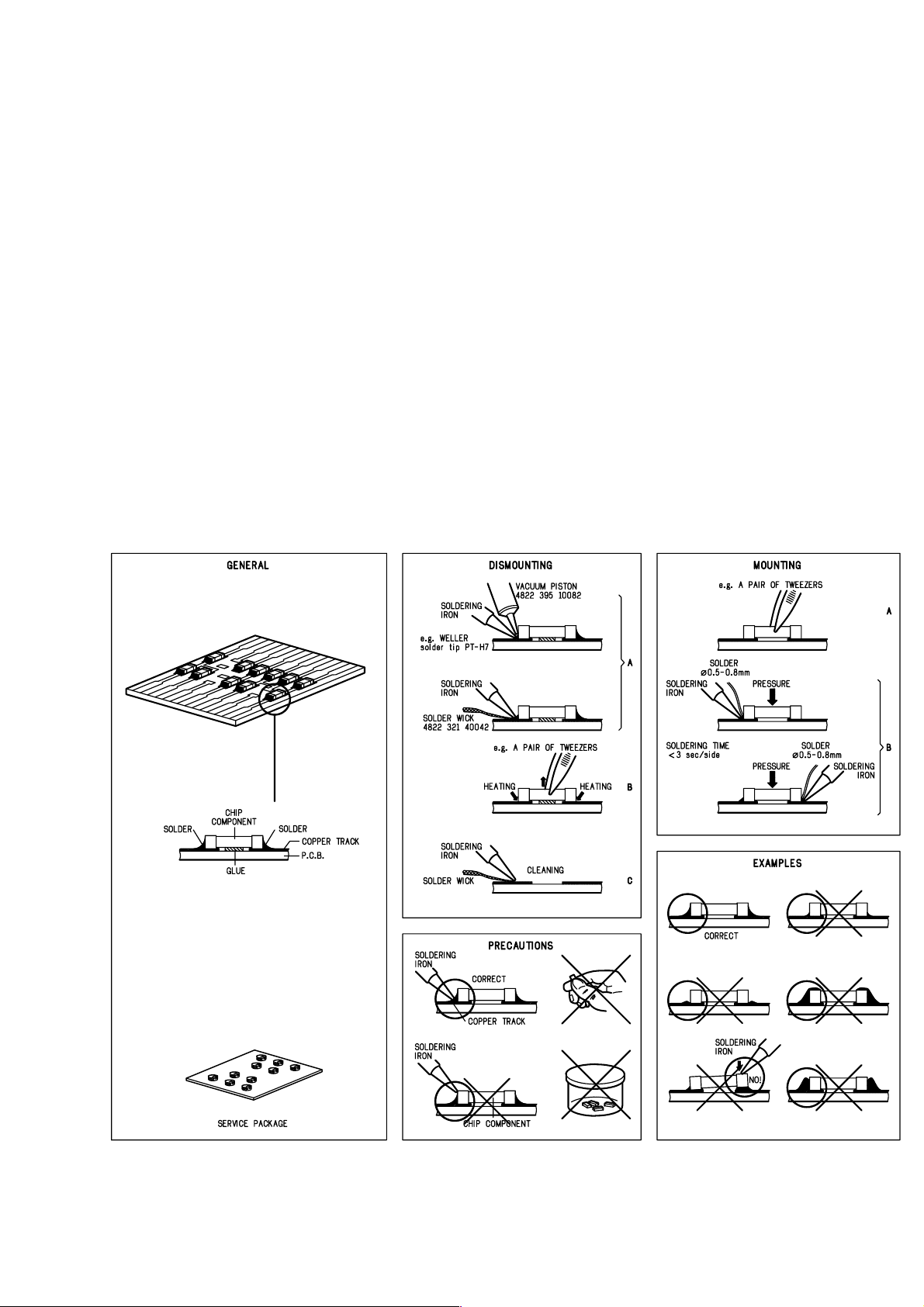
HANDLING CHIP COMPONENTS
ESD Equipment:
Anti-static table mat - large 1200x650x1.25mm ... 4822 466 10953
Anti-static table mat - small 600x650x1.25mm ..... 4822 466 10958
Anti-static wristband .............................................. 4822 395 10223
Connector box (1MΩ) ............................................ 4822 320 11307
Extension cable
(to connect wristband to conn. box) .................. 4822 320 11305
Connecting cable
(to connect table mat to conn. box) .................. 4822 320 11306
Earth cable (to connect product to mat or box) .... 4822 320 11308
Complete kit ESD3
(combining all above products) ......................... 4822 320 10671
Wristband tester .................................................... 4822 344 13999
1-6
GB
All ICs and many other semi-conductors are
susceptible to electrostatic discharges (ESD).
Careless handling during repair can reduce life
drastically.
When repairing, make sure that you are
connected with the same potential as the mass
of the set via a wrist wrap with resistance.
Keep components and tools also at this
potential.
Tous les IC et beaucoup d’autres
semi-conducteurs sont sensibles aux
décharges statiques (ESD).
Leur longévité pourrait être considérablement
écourtée par le fait qu’aucune précaution n’est
prise à leur manipulation.
Lors de réparations, s’assurer de bien être relié
au même potentiel que la masse de l’appareil et
enfiler le bracelet serti d’une résistance de
sécurité.
Veiller à ce que les composants ainsi que les
outils que l’on utilise soient également à ce
potentiel.
F
WARNING
ATTENTION
ESD
D
WARNUNG
Alle ICs und viele andere Halbleiter sind
empfindlich gegenüber elektrostatischen
Entladungen (ESD).
Unsorgfältige Behandlung im Reparaturfall kan
die Lebensdauer drastisch reduzieren.
Veranlassen Sie, dass Sie im Reparaturfall über
ein Pulsarmband mit Widerstand verbunden
sind mit dem gleichen Potential wie die Masse
des Gerätes.
Bauteile und Hilfsmittel auch auf dieses gleiche
Potential halten.
NL
Alle IC’s en vele andere halfgeleiders zijn
gevoelig voor electrostatische ontladingen
(ESD).
Onzorgvuldig behandelen tijdens reparatie kan
de levensduur drastisch doen verminderen.
Zorg ervoor dat u tijdens reparatie via een
polsband met weerstand verbonden bent met
hetzelfde potentiaal als de massa van het
apparaat.
Houd componenten en hulpmiddelen ook op
ditzelfde potentiaal.
Tutti IC e parecchi semi-conduttori sono
sensibili alle scariche statiche (ESD).
La loro longevità potrebbe essere fortemente
ridatta in caso di non osservazione della più
grande cauzione alla loro manipolazione.
Durante le riparazioni occorre quindi essere
collegato allo stesso potenziale che quello della
massa dell’apparecchio tramite un braccialetto
a resistenza.
Assicurarsi che i componenti e anche gli utensili
con quali si lavora siano anche a questo
potenziale.
WAARSCHUWING
I
AVVERTIMENTO
GB
Safety regulations require that the set be restored to its original
condition and that parts which are identical with those specified,
be used
!
Safety components are marked by the symbol
.
NL
Veiligheidsbepalingen vereisen, dat het apparaat bij reparatie in
zijn oorspronkelijke toestand wordt teruggebracht en dat onderdelen,
identiek aan de gespecificeerde, worden toegepast.
De Veiligheidsonderdelen zijn aangeduid met het symbool
!
F
Les normes de sécurité exigent que l’appareil soit remis à l’état
d’origine et que soient utiliséés les piéces de rechange identiques
à celles spécifiées.
Less composants de sécurité sont marqués
!
D
Bei jeder Reparatur sind die geltenden Sicherheitsvorschriften zu
beachten. Der Original zustand des Geräts darf nicht verändert werden;
für Reparaturen sind Original-Ersatzteile zu verwenden.
!
Sicherheitsbauteile sind durch das Symbol
markiert.
I
Le norme di sicurezza esigono che l’apparecchio venga rimesso
nelle condizioni originali e che siano utilizzati i pezzi di ricambio
identici a quelli specificati.
Componenty di sicurezza sono marcati con
!
CLASS 1
LASER PRODUCT
GB
Invisible laser radiation when open.
Avoid direct exposure to beam.
Osynlig laserstrålning när apparaten är öppnad och spärren
är urkopplad. Betrakta ej strålen.
SF
Avatussa laitteessa ja suojalukituksen ohitettaessa olet alttiina
näkymättömälle laserisäteilylle. Älä katso säteeseen!
DK
Usynlig laserstråling ved åbning når sikkerhedsafbrydere er
ude af funktion. Undgå udsaettelse for stråling.
S
Warning !
Varning !
Varoitus !
Advarse !
GB
After servicing and before returning set to customer perform a leakage
current measurement test from all exposed metal parts to earth ground to
assure no shock hazard exist. The leakage current must not exceed
0.5mA.
F
"Pour votre sécurité, ces documents doivent être utilisés par
des spécialistes agréés, seuls habilités à réparer votre
appareil en panne".
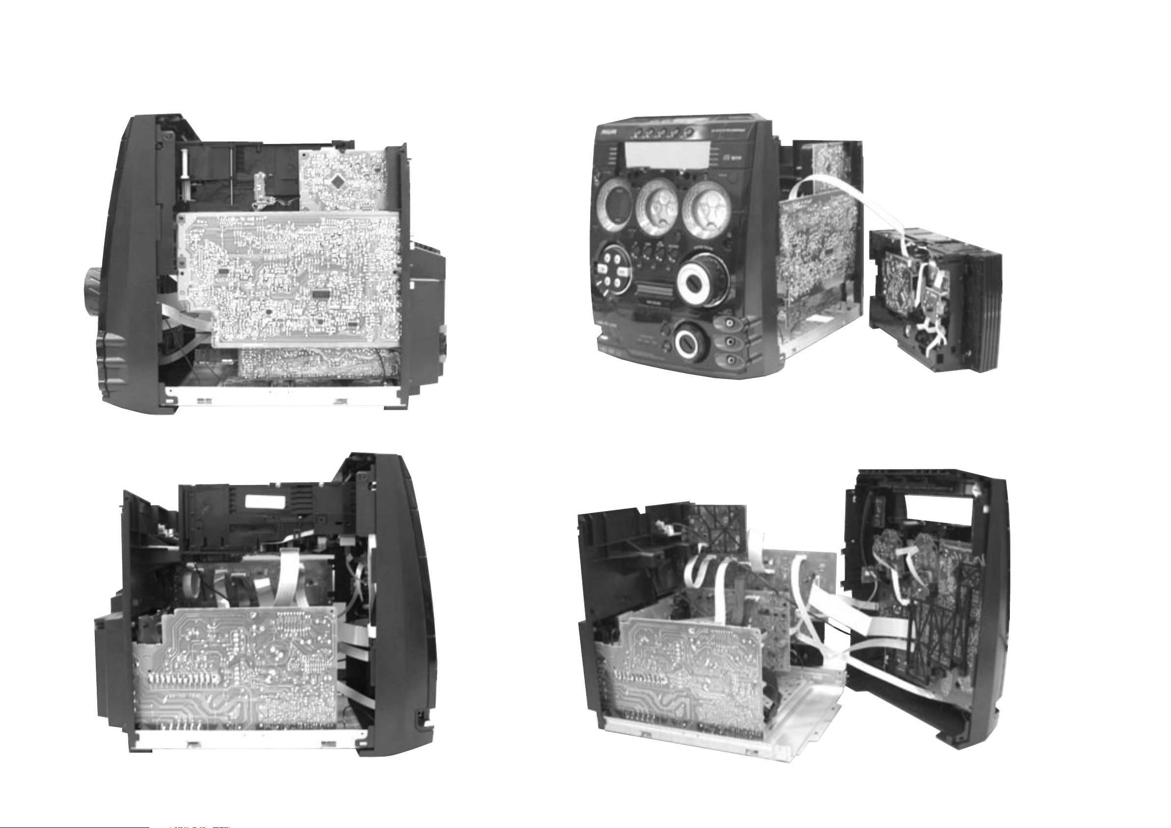
DISMANTLING INSTRUCTIONS
2-1 2-1
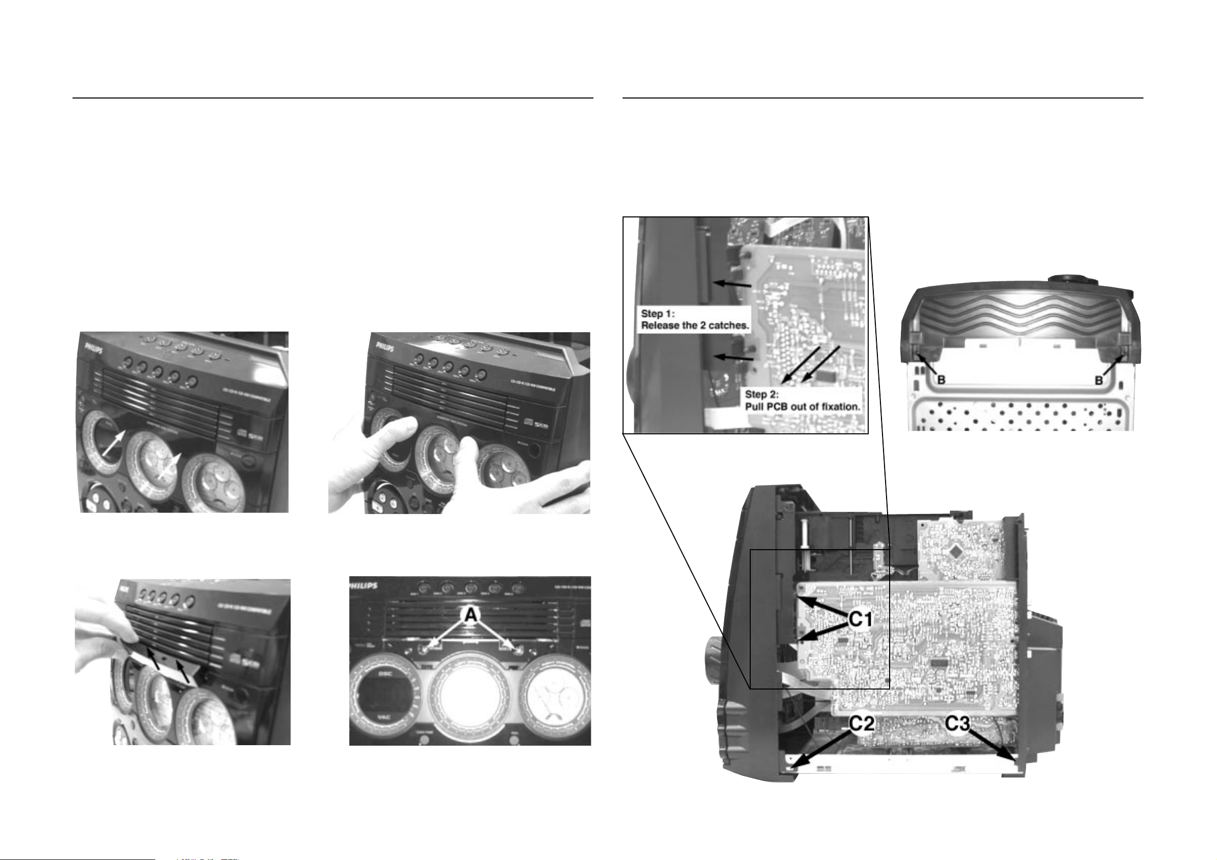
Dismantling of the 5DTC Module
1) Loosen 4 screws to remove the Cover Top (pos 255) by
sliding it out towards the rear before lifting up.
- 2 screws on the rear
- 1 screw each on the left & right side
2) Loosen 3 screws each to remove the Panel Left (pos 253)
and Panel Right (pos 254). The Panels are removed by
sliding it towards the rear and outwards.
- 2 screws on the rear
- 1 screw on the side
3) To loosen the Panel Front Display (pos 120), you have to
press in the correct direction and position as shown in
Figure 1 and Figure 2. Once the Panel Front Display is
loosen, remove it out in the direction as shown in Figure 3.
4) Loosen 4 screws A (see Figure 4 and Figure 16) to remove
the 5DTC Module (pos 1105).
- 2 screws on the front
- 2 screws on the rear
Note : For information on the 'Emergency opening of the
trays' of the 5DTC Module, refer to Chapter 10
(Page 10-7).
Detaching the Front Panel assembly from the Bottom/Rear assembly
1) Remove 2 screws B (pos 226) as shown in Figure 5 from
the bottom of the Cabinet Front (pos 101).
2) Release the fixation of the AF Board (pos1102-A) to
Bracket CDC Right (pos 186) by releasing the 2 catches
C1 (see Figure 7) and pulling the AF Board outwards as
shown in Figure 6.
3) Uncatch 2 catches C2 (see Figure 7) on the left & right
sides of the Cabinet Front (pos 101) and slides the Front
Panel assembly out towards the front.
Figure 1
Figure 2
Figure 6
Figure 5
Figure 3
Figure 4
Figure 7
DISMANTLING INSTRUCTIONS
2-2
2-2
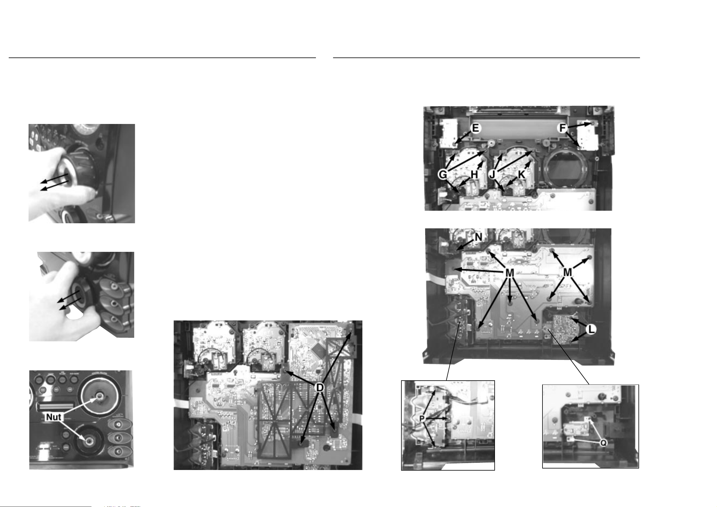
Dismantling of the Front Control Board and Front Display Board
1) The Knob Volume Rotary (pos 164) can be remove by
pulling it out in the direction as shown in Figure 8.
2) The Knob Game Sound Control (pos 176) can be remove
by pulling it out in the direction as shown in Figure 9.
Figure 8
3) Loosen 4 screws D (see Figure 11) to remove the Bracket
4) Loosen 1 screw E (see Figure 12) to remove the IR Eye
5) Loosen 2 screws F (see Figure 12) to remove the ECO
6) Loosen 3 screws G (see Figure 12) to remove the
7) Loosen 3 screws J (see Figure 12) to remove the Bracket
8) Loosen 2 screws L (see Figure 13) to remove the USB PC
PCB Front Display (pos 183) and Front Display Board
(pos 1101-A).
Board (pos 1107-H).
Power Board (pos 1107-E).
Bracket VU Meter 2 (pos 136) and loosen 2 screws H to
remove the VU Meter Right Board (pos 1107-D) from the
Bracket VU Meter 2.
VU Meter 1 (pos 129) and loosen 2 screws K to remove
the VU Meter Left Board (pos 1107-C) from the Bracket
VU Meter 1.
LINK Board (pos 1104).
Dismantling of the Front Control Board and Front Display Board
11) Loosen 3 screws P (see Figure 14) to remove the Game
Port Board (pos 1107-G).
Figure 12
Figure 13
12)Loosen 2 screws Q (see Figure 15) to remove the USB
LED Board (pos 1107-F).
Figure 9
9) Loosen 9 screws M (see Figure 13) and loosen the 2 nuts
(see Figure 10) to remove the Front Control Board (pos
1107-A).
10)Loosen 1 screw N (see Figure 13) to remove the
Headphone Board (pos 1107-B).
Figure 10
Figure 11 Figure 15
Figure 14
DISMANTLING INSTRUCTIONS
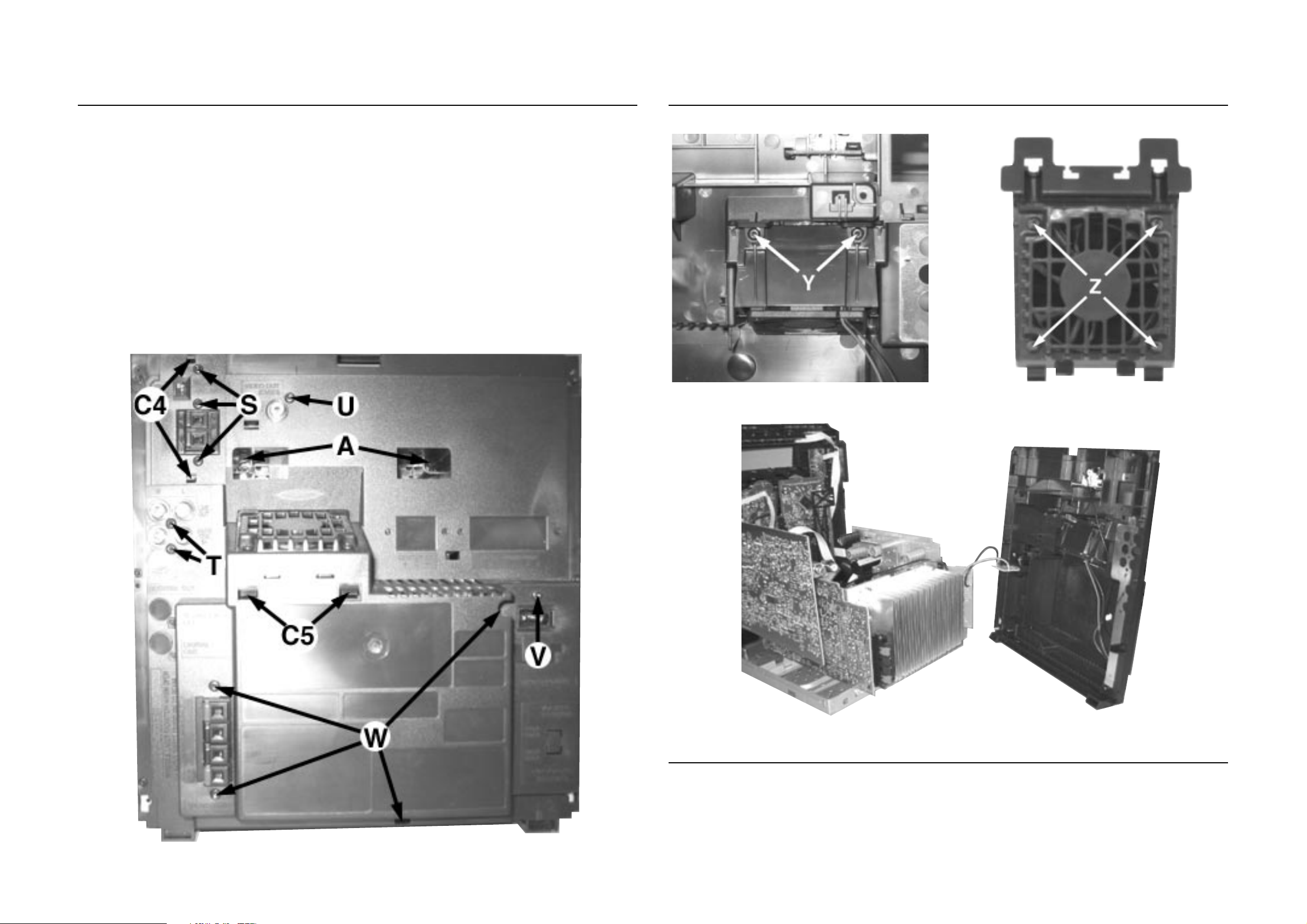
2-3 2-3
Dismantling of the Rear Panel assembly
1) Loosen 3 screws S and 2 catches C4 (see Figure 16) to
remove the Tuner Board assembly.
2) Loosen 2 screws T (see Figure 16) to free the AF Board
(pos 1102-A).
3) Loosen 1 screw U (see Figure 16) to remove the Video
Cinch Out Board (pos 1102-B).
4) Loosen 1 screw V (see Figure 16) to free the Mains
Socket Board (pos 1106-1001-B).
5) Loosen 4 screws W (see Figure 16) and 2 catches C3
(see Figure 7) to remove the Panel Rear (pos 256) by
sliding it out towards the rear (see Figure 19).
Note : Tuner Board assembly and Mains Socket Board
can also be remove together with the Panel Rear.
6) Loosen 2 screws Y (see Figure 17) and 2 catches C5 (see
Figure 16) to remove the Bracket Fan (pos 266).
7) Loosen 4 screws Z (see Figure 18) to remove the Fan
(pos 1121) from the Bracket Fan (pos 266).
Dismantling of the Rear Panel assembly
Figure 17
Figure 18
Figure 16
Repair Hints
1) During repair it is possible to disconnect the ECO6 Tuner
board and/or 5DTC Module completely unless the fault is
suspected to be in that area. This will not affect the
performance of the rest of the set.
Figure 19
Note: The flex cables are very fragile, care should be taken
not to damage them during repair. After repair, be
very sure that the flex cables are inserted properly
into the flex sockets before encasing, otherwise faults
may occurs.
2-4 2-4
DISMANTLING INSTRUCTIONS
Service position A Service position B
Service position C
3-1 3-1
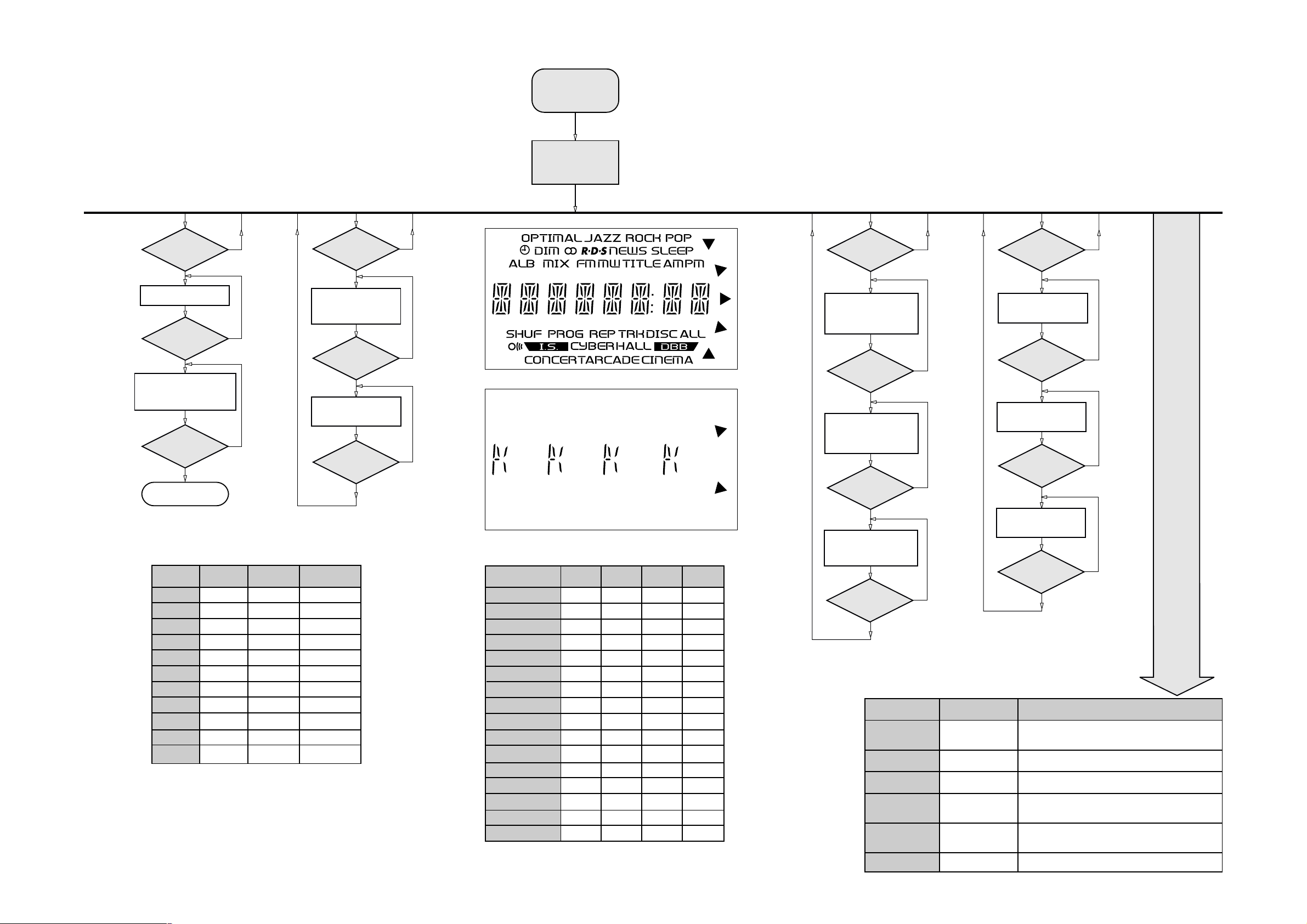
SERVICE TEST PROGRAM
TUNER
TEST
TUNER
Button pressed?
Y
Display Tuner Version
"ccc"
TUNER
Button pressed?
Y
Service frequencies are
copied to the RAM (see Table 1)
Tuner works normally except:
PROGRAM button
Disconnect
Mains cord ?
Y
Service Mode left
N
N
N
QUARTZ
TEST
O
Button pressed?
Y
Display shows
Output at (Front Display Board)
Output at (Front Display Board)
pin 19 of uP = 2,929.6875Hz
32K
pin 19 of uP = 2048Hz
O
Button pressed?
Y
Display shows
12M
9
Button pressed?
Y
To start service test program
N
N
N
& AUX
hold
™
depressed while
plugging in the mains cord
Display shows the
ROM version
"S-Vyy"
(Main menu)
Figure 1
S refers to Service Mode
V refers to Version
yy refers to Software version number of the uProcessor
(counting up from 01 to 99)
DISPLAY
TEST
VAC
Button pressed?
Y
Display shows Figure 1
and switch all LEDs on
(except ECO POWER LED), with
full deflection on VU meter Right
& 1/3 deflection on VU meter Left.
VAC
Button pressed?
Y
Display shows Figure 2
and switch alternate LEDs on
(see Table 2), with
1/3 deflection on VU meter Right
& full deflection on VU meter Left.
VAC
Button pressed?
ADC
TEST
N
N
N
PLAY
Button pressed?
Y
Display shows "ADC1 Value"
for ADC1
(Input Line - IoSA2)
PLAY
Button pressed?
Y
Display shows "ADC2 Value"
for ADC2
(Input Line - IoSA1)
PLAY
Button pressed?
Y
N
N
N
PRESET
1
2
3
4
5
6
7
8
9
10
11
Note:
* Depending on the selected grid frequency (9 or 10kHz).
By holding the TUNER and
on the Mains supply, the tuning grid frequency is toggled between
9kHz and 10kHz for the Oversea (/21) version.
Europe
"EUR"
87.5MHz
108MHz
531kHz
1602kHz
558kHz
1494kHz
153kHz
279kHz
198kHz
98MHz
87.5MHz
USA
"USA"
87.5MHz
108MHz
530kHz
1700kHz
560kHz
1500kHz
98MHz
87.5MHz
87.5MHz
87.5MHz
87.5MHz
Table 1
R
buttons depressed while switching
Oversea
"OSE"
87.5MHz
108MHz
531/530kHz*
1602/1700kHz*
558/560kHz*
1494/1500kHz*
87.5/98MHz*
87.5MHz
87.5MHz
87.5MHz
98/87.5MHz*
Figure 2
ON
ON
ON
ON
ON
FW-C579
FW-M567
-
-
-
-
ON
OFF
ON
OFF
ON
OFF
ON
OFF
ON
OFF
OFF
OFF
LEDs
CD
TUNER
AUX / GAME
USB PC LINK
DISC 1
DISC 2
DISC 3
DISC 4
DISC 5
^^ MAX 1 (WOOX 1)
^^ MAX 2 (WOOX 2)
^^ MAX 3 (WOOX 3)
SPEED
PUNCH
BLAST
USB Indicator
^^ MAX - FW-C557, FW-C577, FW-C579, FW-M567
WOOX - FW-C777, FW-M777
FW-C557
-
-
-
-
-
-
-
-
-
OFF
ON
OFF
ON
OFF
OFF
-
FW-C577
OFF
OFF
OFF
OFF
OFF
OFF
OFF
Table 2
Y
No Display shows
and switch all LEDs off, with
2/3 deflection on VU meter Right
& 2/3 deflection on VU meter Left.
FW-C777
FW-M777
-
-
-
-
OFF
ON
OFF
OFF
9
Button pressed?
Y
N
ON
OFF
Display shows "ADC3 Value"
for ADC3
(Input Line - IoAmNTC)
9
Button pressed?
Y
ADC Test is used for checking the
ADC inputs to the microprocessor.
The display shows an ADC value
between 0 and 255 for an input
signal between 0 and 5V.
N
Various
other Tests
ON
OFF
ON
OFF
ON
OFF
ON
OFF
OFF
OFF
TEST
EEPROM TEST A test pattern will be sent to the EEPROM.
EEPROM FORMAT
TEST
DEMO TOGGLE
ROTARY
ENCODER TEST
MICRONAS
FIRMWARE
VERSION
LEAVE SERVICE
TEST PROGRAM
Activated with
R
to Exit
9
Q
^^ MAX (WOOX 2)
Rotary Volume
Knob
USB PC LINK
9
to Exit
Disconnect
mains cord
ACTION
"PASS" is displayed if the uProcessor read back the test pattern
correctly, otherwise "FAIL" will be displayed.
Load default data. Display shows "NEW" for 1 second.
Caution! All presets from the customer will be lost!!
Pressing this button will toggle between DEMO ON and DEMO
OFF. The DEMO status will scroll once across the Display.
Display shows value for 2 seconds.
Values increases or decreases until Volume Maximum (VOL
MAX) or Volume Minimum (VOL MIN) is reached.
To read out the Firmware Version of IC UAC3553 on the USB
PC LINK Board.
Display shows "Vxxxx" (xxxx = Firmware Version number).
Mini 2003_FW-C/M 5xx/7xx_Service Test Program (dd wk0306)
3-2 3-2
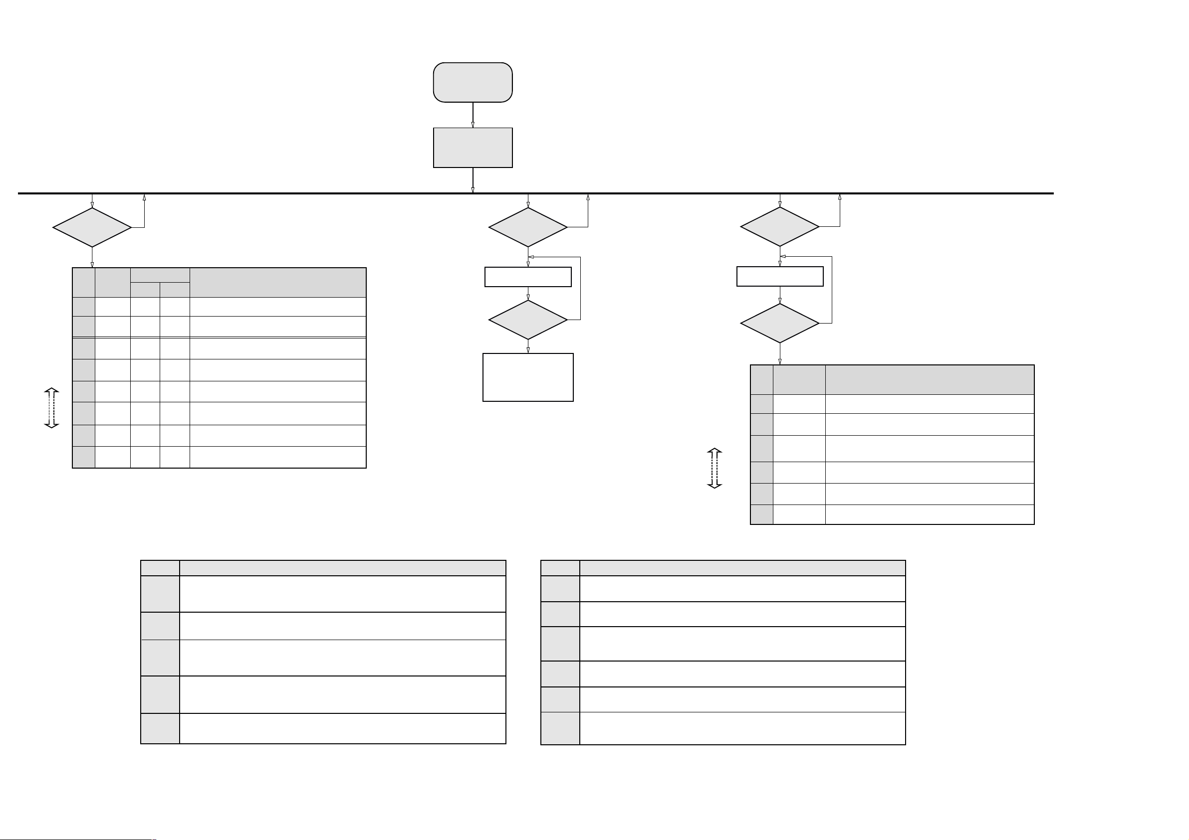
SERVICE TEST PROGRAM
5DTC CONTROL &
MP3 CD MODULE
TEST
N
(For MP3 set only)
Note : Disc should be available on the tray before entering the Service Test Mode.
DISPLAY
TI-Vnn
TI BUS
TI SLD I
TI SLD O
TI FOC
MESSAGE
OKAY
-
-
-
BUS OK
-
-
FOC OK
** Choose
level
by pressing
Q
R
CD
Button pressed?
Y
STEP
5DTC-Vnn
1
MP3CD’02
2
**3
**4
**5
**6
**7
ERROR
5DTC-ER
-
-
BUS ER
-
-
FOC ER
ACTION
Version of the 5DTC control software (nn = Version Number).
Indicates the module used.
Version of the MPEG software (nn = Version Number).
Communication test between the Main uP and CD Module
CD SLEDGE MOTOR is moved in.
CD SLEDGE MOTOR is moved out.
FOCUS SERVO Test.
Press
9
to exit
To start service test program
& AUX
hold
™
depressed while
plugging in the mains cord
Display shows the
ROM version
"S-Vyy"
(Main menu)
SERVICE PLAY MODE
(For non MP3 set only)
STANDBY ON
Button pressed?
Set is in Service PLAY Mode
Button pressed?
Display shows "5DTC-Vnn" -
Version of 5DTC control software
(nn = Version Number).
DTC works as in normal operation.
In case of failures, error
codes according to Table 3A and
Table 3B will be displayed.
The Service Play Mode is intended
to detect and identify the failures
in the CD Mode.
In this mode the DTC works as in
normal operation. The electronics
will still function even when an error
is detected so that repair activities
can be carried out.
S refers to Service Mode
V refers to Version
yy refers to Software version number of the uProcessor
(counting up from 01 to 99)
N
Y
CD
Y
N
GAME PORT
TEST
Choose desired
background source
by pressing button
" MIX-IT "
GAME
Button pressed?
Y
Display shows "GAME PORT"
MIX-IT
Button pressed?
Y
STEP
DISPLAY
(SCROLL ONCE)
MIX-CD
1
MIX-TU
2
MIX-USB
3
MIX-AUX
4
N
N
ACTION
Select CD as background sound source. Press PLAY to play the track.
Select TUNER as background sound source.
Select PC-LINK (for set with PC-LINK) as background sound source.
Press PLAY to play the track.
Select AUX as background sound source.
Error code
E1000
E1001
E1002
E1003
E1005
Error Description
Focus Error
Triggered when the focus cannot be found within a certain time when starting up the CD, or if the focus
is lost for more than a certain time during playing of CD.
Radial Error
Triggered when the radial servo is off-track for a certain time during playing of CD.
Sledge In Error
The sledge did not reach its inner position (inner-switch is still close) before approximately 6 seconds
have passed by. Inner-switch or sledge motor problem.
Sledge Out Error
The sledge did not come out of its inner position (inner-switch is still open) before approximately 250ms
have passed by. Inner-switch or sledge motor problem.
Jump Error
Triggered in normal play when the jump destination could not be found within a certain time.
Table 3A
Error code
E1006
E1007
E1008
E1020
E1061
E1079
MIX-OFF
5
No mixing.
Disconnect mains cord to exit
Error Description
Subcode Error
Triggered when a new subcode was missing for a certain time during playing of CD.
PLL Error
The Phase Lock Loop could not lock within a certain time.
Turntable Motor Error
Generated when the CD could not reached 75% of speed during start-up within a certain time. Disc
motor problem.
Focus Search Error
The focus point has not been found within a certain time.
The tray could not enter the inside position and is opening again. This can happen if the tray is blocked
such that it cannot go fully inside, or if the 5DTC control module is defective and never closes.
The tray could not reach the outside position and is stopped at its blocked position. This can happen if
the tray is blocked such that it cannot go fully outside, or if the 5DTC control module is defective and
never opens.
Table 3B
Mini 2003_FW-C/M 5xx/7xx_Service Test Program (dd wk0306)
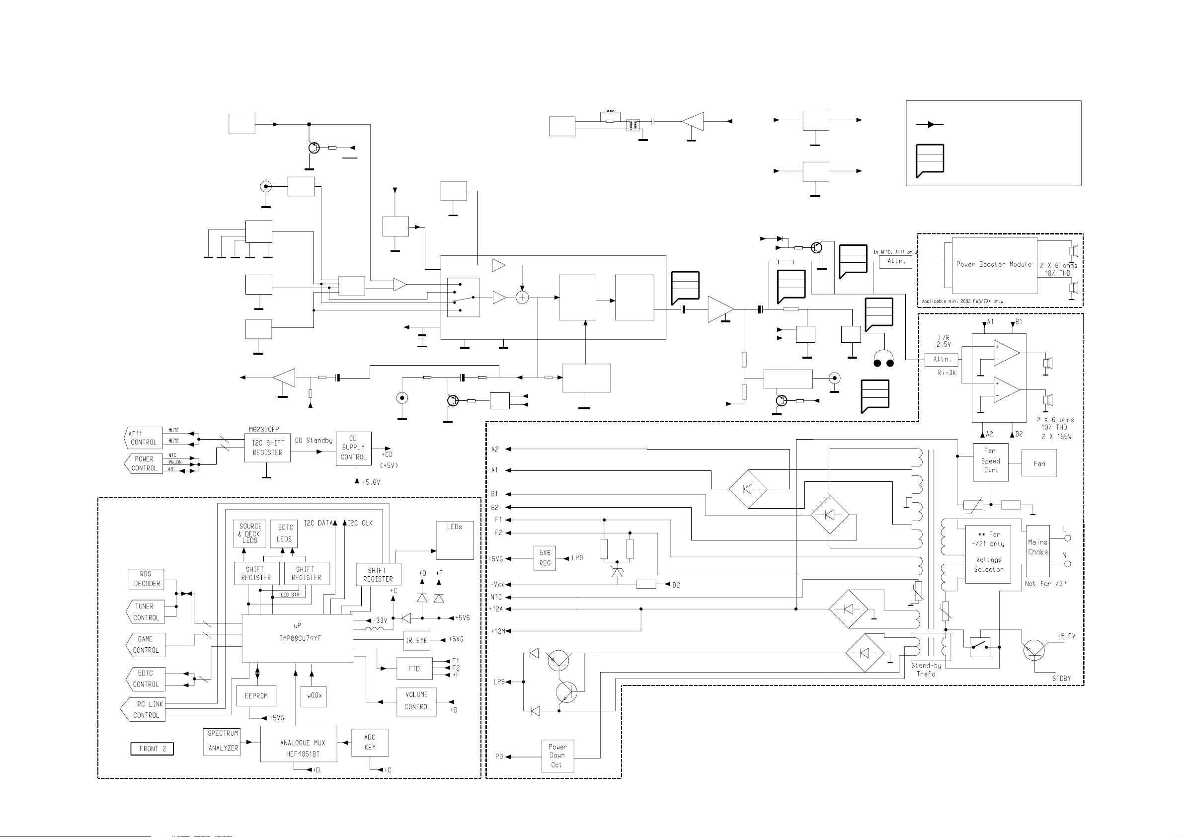
SET BLOCK DIAGRAM
4-1
4-1
AUX 640mV
D
D
GAME
PORT
GAME 310mV
5DTC
M
DIG
TUNER
PC-LINK
SA_OUT
2.1V
Attn
-8.5 dB
75 ohm
Vpp 0.5V
DIG
OUT
Game
A
DIG
+12V_A
MIC
COAX1 (FROM 5DTC)
DIG
-VKK
LOW_PW_SPLY
-CMOS
REG.
+5V
REG.
-CMOS
-9V
A
+5V6
CON
NOTE :
MAIN SIGNAL PATH
MEASUREMENTS ARE IN AUX MODE :
LEVELS AT MAX VOL
XX mV
YY dBA
S/N AT 500mW
ZZ dB
HEADROOM (1% THD) WRT TO LEVEL AT MAX VOL
A
A
A
Line Out
500mV
+9V1
REG.
A
VREF
Mute_SW
Mute_SW_FR
DPL/
IS
Interface
Audio
Signal
Proc.
200mV
76dBA
16dB
H/P Amp
2.50V
85dBA
3dB
A
-Vkk
A
A
AD
Mute
CCT
A
-Vkk
Mute2
FIS or
SIS Filter
CCT
From other
A
Chan.
Mute1
SUBWOOFER
CCT
A
Mute
CCT
Mute_SW_FR
A
A
S/W OUT
1.90V
67dBA
3dB
H/P
A
A
650mV
78dBA
3.2dB
0.8V
86dBA
3.5dBA
900mV
H/P
250mV
A
125mV
HEF
4052
A
125mV
A
A
From other
Chan.
D
(Blue Strip)
(wOOx)
(BassTreble)
Block Diagram_3139 119 36101 dd wk0310
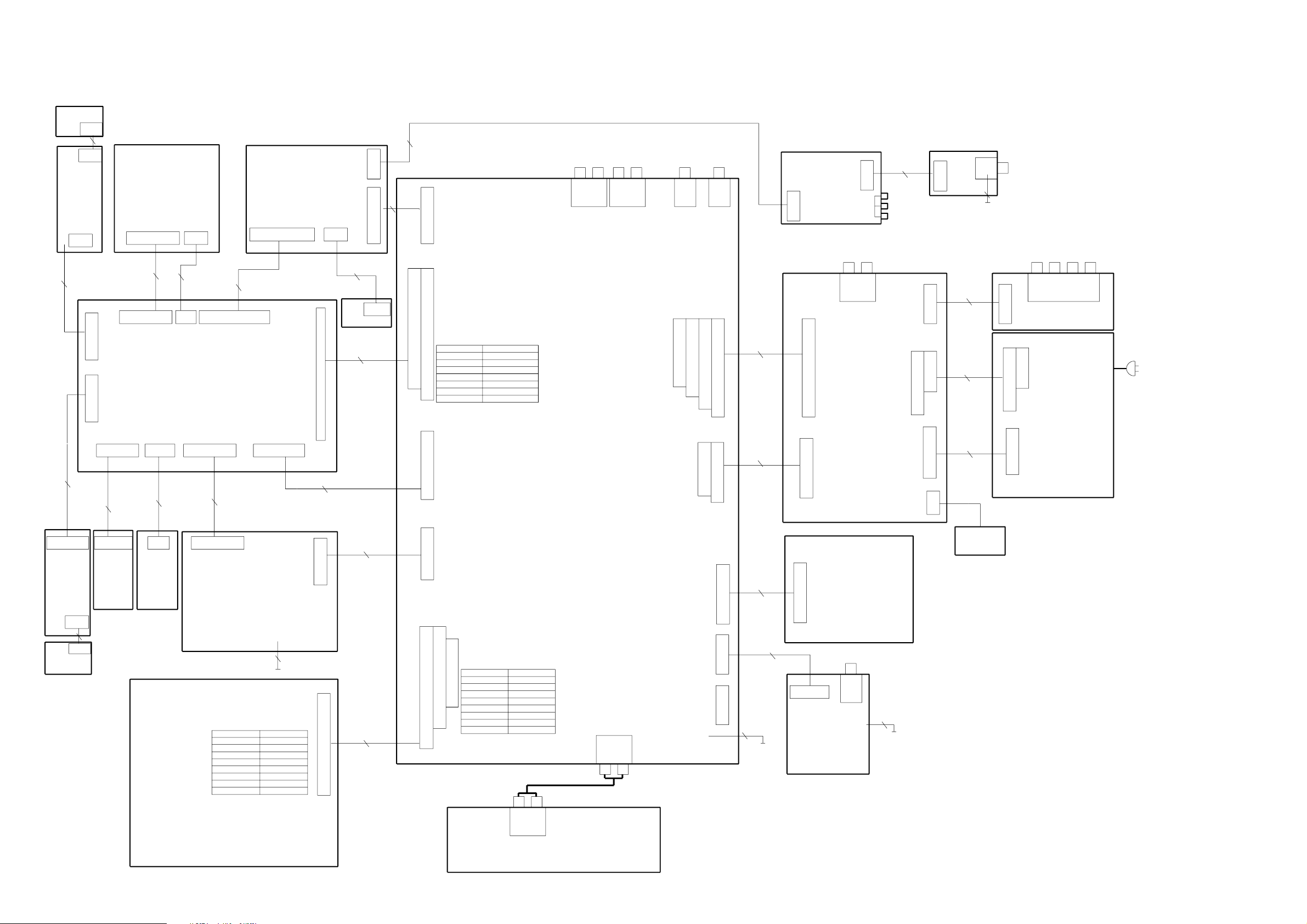
SET WIRING DIAGRAM
VU Meter
Housing
Left
VU Meter
( 1107-C )
1
HR 3p/220/3p OE
(37301)
1
1830
HM 3p
GND_D
VUmeter
VU Meter
Right
( 1107-D )
1
VU Meter
Housing
Right
T136
T135
Hot Melt
1811
2p EH-S
1
GND
Left
GND_D
+5V6
VUmeter
1810
HM 3p
HR 3P/220/3P OE
(37301)
GND_D
1405
1
1406
GND_D
EH-S 3P EH 3p-S
+5V6
FFC 5p Vertical
15
1
FFC 5p Hor.
+5V6
+5V6
Power
( 1107-E )
GND
1831
2p EH-S
8416
HR 2p/100/2p OE
(37131)
Hot Melt
T151
T150
8401
HR 2p/100/2p OE
(37131)
5DTC Key
( 1101-B )
DTC5Lit
DTC3Lit
DTC4Lit
DTC2Lit
1850
FFC 8p Horizontal
1
8404
FFC AD 08p
300 Fold C
(102511)
8
1404
FFC 8p Vertical FFC 10p Vertical
DTC2Lit
DTC3Lit
DTC5Lit
DTC1Lit
DTC4Lit
Key_0
GND_B
( 1107-H )
+5V6_Con
1
1
IR Eye
Receiver
1407
8410
FFC AD 5p 180
Fold C
(102501)
1880
+L
GND
ECO
5DTC / 3CDC
DTC1Lit
GND_D
GND-B
Key_0
1857
HM 2p
8
HR 02P/280/02P OE
(37181)
1
1403
EH 2p
GND-B
Key_0
GND_D
Front Display / uP
( 1101-A )
uAC_IRQ
1409
EH-S 3p
1860
HM
VS
Out
uAC_READY
FFC 8p Vertical
1
HR 3p/280/3p OE
(37311)
1
FFC 8p Horizontal
Gnd
uAC_IRQ
( 1105 )
1
Key1
Key2
GND-B
GND
IIC_CLK
+F
1408
8412
FFC AD 08p 140
(35030)
1703
+F
GND
uAC_READY
+A
TRAY_I2C_SDA
TRAY_I2C_SCL
TRAY_IRQ
CD_PORE
uP_FRAME
uP_CLK
GND_D_CD
uP_DATA
1
8405
FFC AD 10p 120
(35280)
1402
GND
+5V6
SRData1
LEDShStr
LEDShClk
IIC_DATA
IIC_SUSP
N.C
8
1
8
N.C
IIC_CLK
IIC_DATA
IIC_SUSP
USB PC LINK
( 1104 )
TI
4-2
Front Control
( 1107-A )
Key2
+5V6
GND-B
LEDShClk
ShData
GND
Key1
FFC 10p Horizontal
Vol_A
TU_STEREO
FFC 9p Horizontal
+A
TRAY_I2C_SDA
TRAY_I2C_SCL
TRAY_IRQ
CD_PORE
CD_RAB
CD_SILD
GND_D_CD
CD_SICL
LEDShStr
1600
10
GND_D_I2C
I2C_DATA
I2CCLOCK
Vol_B
GND_D
+5V6_CON
+12V_M
CDRAB
TRAY_IRQ
TRAY_I2C_SCL
GND_D_CD
TRAY_I2C_SDA
CDPORE
CDSILD
CDSICL
1400
GND_A
USB_L
+12V_A
USB_R
8901
SRA 1P/180/1P STO-8
(102631)
CD_Left
GND_A_CD
CD_Right
+5V_CD
GND_M
5DTC
+5V6
GM_RIGHT
USB_LIT
Vol_B
Vol_A
1603
HM
1
HR 2p/100/2p OE
(37131)
1401
1
NTC
-Vkk
F1
F2
FFC 19p Horizontal
19
9
8413
FFC AD 9p 340
(35400)
N.C
N.C
1
1702
FFC 7p Horizontal
N.C
1
1824
FFC 15p Horizontal
15
GND_A
GM_LEFT
GM_L
GND_A
+12V
GM_R
EN22
GND-B
EN11
A22
A11
USB
LED
( 1107-F )
8408
FFC AD 19p 280
(102491)
8415
FFC AD 07p 280
(34600)
8417
FFC AD 15p 280
(36150)
1
HM
1604
1
1602
FFC 8p Horizontal
1850
2p EH-T
HR 03p/80/03p OE
(37251)
8407
(34920)
FFC BD 8p 220
1
1405
19
1
9
1
7
1
1692
FFC 8p Horizontal
NTC
GND_D_I2C
I2C_DATA
I2CCLOCK
GND_D
+5V6_CON
+12V_M
+5V6
1401
-Vkk
F1
F2
CDRAB
FFC 19p Vertical
FFC 16p Vertical
TRAY_IRQ
TRAY_I2C_SCL
GND_D_CD
TRAY_I2C_SDA
CDPORE
CDSILD
CDSICL
TU_STEREO
TU_CLK
TU_DATA
TU_ENAB
GND_A_TU
1402
SA_LEFT
SA_RIGHT
PWR_DN
FFC 9p Vertical
L_PWR_CTRL
GND
N.C
N.C
GND_A
USB_L
1531
+12V_A
USB_R
FFC 7p Vertical
N.C
1522 1523
1525
1
1525
1523
1522
FFC 9p Vertical
FFC 19p Vertical
FFC 15p Vertical
9
15
19
CD_SH_DATA
CD_SH_CLK
CD_SH_STR
GND_D_CD
SW_INFO
SICL
SILD
DSA_STB / GND_D
CD_Left
GND_A_CD
CD_Right
+5V_CD
GND_M
+12V_M
TRAY_I2C_SDA
TRAY_I2C_SCL
TRAY_IRQ
CDPORE
CDRAB
CDSILD
GND_D_CD
CDSICL
GND_D_CD
COAX1
COAX2
SHIELD
GND_D_COAX
Power Booster In
( 1102-A )
SW_INFO
CD_SH_STR
CD_SH_CLK
SICL
CD_SH_DATA
SILD
GND_D_CD
CDPORE
GND_D_CD
1501
AF11
# Power Booster Out
AUX IN
LINE OUT
15041
LOW_PWR_CTRL
VCD_ON/CDR_ON
# 1604
AMP_LEFT
GND_AA
AMP_RIGHT
NTC
PWR_DN
CLIPPING
AMP_ON
-VKK
AMP_CS_DC
DVD_ON
LOW_PWR_SPLY
OUT
SUBWOOFER
1691 1801
1206
FFC 11p Vertical
F1
F2
+12V_A
GND_A
+12V_M
GND_M
+5V6
GND_D
5V_VCD
TU_LEFT
TU_RIGHT
TU_ENAB
TU_DATA
TU_STEREO
HP_LEFT
HP_RIGHT
HP_DET
+12V_A
MIC_DET
SMF 1P/090/1P STO-8
DIGITAL OUT
COAX
1203
1201
1205
FFC 13p Vertical
FFC 12p Vertical
1204
1202
EH-T 7p
7
GND_A
+12V_A
TU_CLK
GND_A
MIC
GND_A
8902
(35531)
1
*8300
FFC AD 11p 220
FFC 14p Vertical
FFC AD 12p 220
*FFC AD 13p 220
11
12
13
14
1
*8301
HR 07p/220/07p HR
EH-T 8p
*HR 08p/220/08p HR
( For VCD only )
8
1
1520
FFC AD 08p 180 (15)
FFC 8p Vertical
8
1
1603
4
FFC 4p Vertical
1
# 1503
FFC 4p Vertical
4
8202
(35351)
or
or
8201
(39031)
or
8601
(102481)
8501
FFC BD 04p 180
(33940)
Game Port
( 1107-G )
1
GM_LEFT
GND_A
1893
3p EH-S
GM_RIGHT
1259/1260/1261 (11p/12p/13p)
1
1259/1260/1261
14
1262/1263 (7p/8p)
1
1262/1263
8
*1310 (8p)
1
1120
FFC 8p Vertical
4
1840
FFC 4p Vertical
GND_A
HP_LEFT
CVBS
GND_D
*1307
AMP_LEFT
GND_AA
AMP_RIGHT
NTC
LOW_PWR_CTRL
PWR_DN
CLIPPING
AMP_ON
-VKK
F1
FFC 11p/12p/13p Vertical
F2
AMP_CS_DC
VCD_ON
DVD_ON
LOW_PWR_SPLY
+11V_A
GND_A
+11V_M
GND_M
+5V6
EH-T 7p/8p
GND_D
L/R + Supply Amp.
5V_VCD
TU_LEFT
GND_A_TU
TU_RIGHT
+12V_A
TU_ENAB
TU_DATA
TU_CLK
TU_STEREO
HP_RIGHT
H/P
1
HP_DET
* Power Board
1841
Headphone
( 1107-B )
4-2
HR 2P/400/2P OE
1
HM
1894
1892
1891
1890
LS
1321
L_PWR_CTRL
( 1106-1002 )
TUNER
ECO6
( 1103 )
8903
SMF 1P/220/1P STO-8
(102641)
(37201)
CVBS
L
R
B1
GND_D
GND_D
B2
A2
+D
GND
+D2
PWR_DN
L_PWR_S
A1
*1302
1250
-VKK
NTC
+FAN
1250
F1
F2
GND
*1308
EH-T 9p
*1304
Video Cinch
Out
1
1800
1330
1
# 1330
EH-T 4p
1251
1
1251
EH-T 6p
1252
1
1252
FFC 7p Vertical
1
1300
2p EH-T
(1102-B)
2p EH-T
8809
SMF 1P/280/1P STO-
(102621)
*1200
HR 04p/340/04p HR
8906
HR 06p/340/06p OE
8909
HR 09p/340/09p OE
*1205
HR 06p/400/06p HR
8203
*8204
FFC AD 07p 340
(35011)
FAN
MOTOR
1803
1
1913
1
VIDEO OUT
(CVBS)
8
( Only for FW-C720 )
1315
EH-T 4p
MATRIX SURROUND
*1203
1912
A1
B1
GND_D
GND_D
1912
6p Dipmate
B2
1913
A2
9p Dipmate
+D
GND
+D2
1914
-VKK
F1
F2
PWR_DN
1914
NTC
L_PWR_CTRL
FFC 7p Vertical
L_PWR_S
*1209
LS SL/SR
Mains Board
( 1106-1001 )
* For PWR2001 Module (30-70W)
Version only.
# Provision.
Power Booster Module
For Mini 2003 FW-C799
Wiring Diagram_3139 119 36091 dd wk0310
5-1 5-1
FRONT CONTROL BOARD
HEADPHONE BOARD - COMPONENT LAYOUT
This assembly drawing shows a summary of all possible versions. For components
used in a specific version see schematic diagram and respective parts list.
3139 113 3513 pt4 dd wk0310
HEADPHONE BOARD - CIRCUIT DIAGRAM
1840 C1 1841 B3
1842 A3 2841 A2 2843 A2 2844 A3 5840 B2 5841 B2 5842 A3 9840 A3
HEADPHONE BOARD - CHIP LAYOUT
This assembly drawing shows a summary of all possible versions. For components
used in a specific version see schematic diagram and respective parts list.
3139 113 3513 pt4 dd wk0310
TABLE OF CONTENTS
Headphone part - Layout & Circuit diagram.................... 5-1
Control part - Component Layout .................................... 5-2
Control part - Chip Layout ............................................... 5-3
Control part - Circuit diagram .......................................... 5-4
ECO Power part - Layout & Circuit diagram ................... 5-5
Game Port part - Layout & Circuit diagram ..................... 5-5
VU Meter (Left) part - Layout & Circuit diagram ............. 5-6
VU Meter Housing (Left) part - Layout & Circuit ............. 5-6
VU Meter (Right) part - Layout & Circuit diagram ........... 5-7
VU Meter Housing (Right) part - Layout & Circuit ........... 5-7
IR Eye part - Layout & Circuit diagram ........................... 5-8
USB LED part - Layout & Circuit diagram ....................... 5-8
Electrical parts list............................................................ 5-9
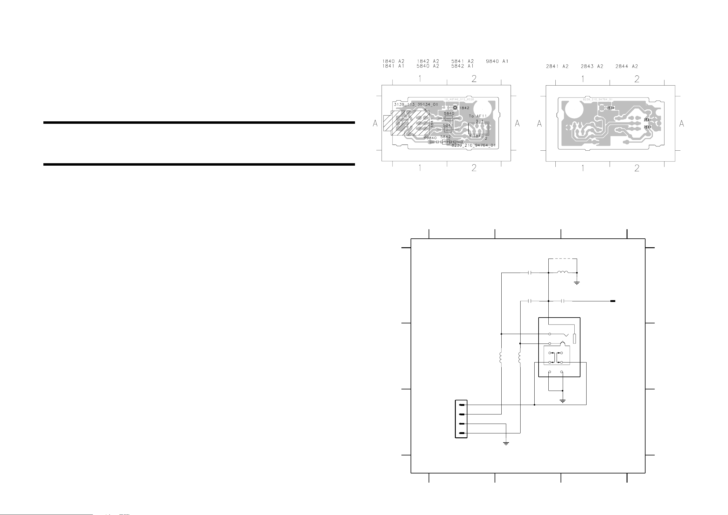
HEADPHONE
A
B
HP_DET
HP_RIGHT
C
HP_GND
HP_LEFT
123
# 9840
5842
2u2
HP
2844
100n
9
7
8
4
5
6
# : Provision
Note : Some values may varies, see respective
1
2
3
HP
parts list for correct value.
1842
RT-01T1
1841
TC38
To AF11 Board
1840
1
2
3
4
FE-BT-VK-N
5840
HP
2u2
5841
2841
22n
2843
22n
2u2
A
B
C
3139 118 56720...8239_210_94764 for 3513 pt4 dd wk0310
123
CONTROL BOARD - COMPONENT LAYOUT
5-2
5-2
This assembly drawing shows a summary of all possible versions. For components used in a specific version see schematic diagram and respective parts list.
3139 113 3513 pt4 dd wk0310
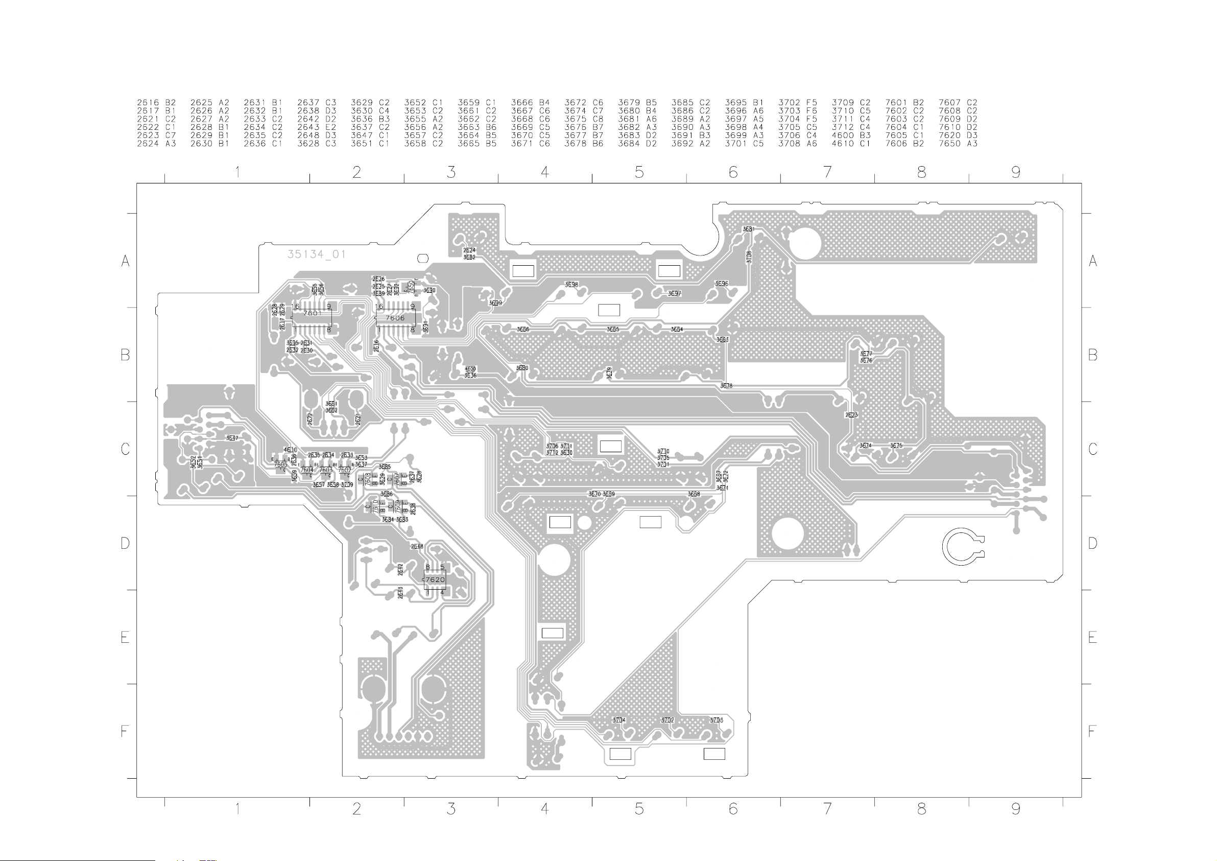
CONTROL BOARD - CHIP LAYOUT
5-3
5-3
This assembly drawing shows a summary of all possible versions. For components used in a specific version see schematic diagram and respective parts list.
3139 113 3513 pt4 dd wk0310
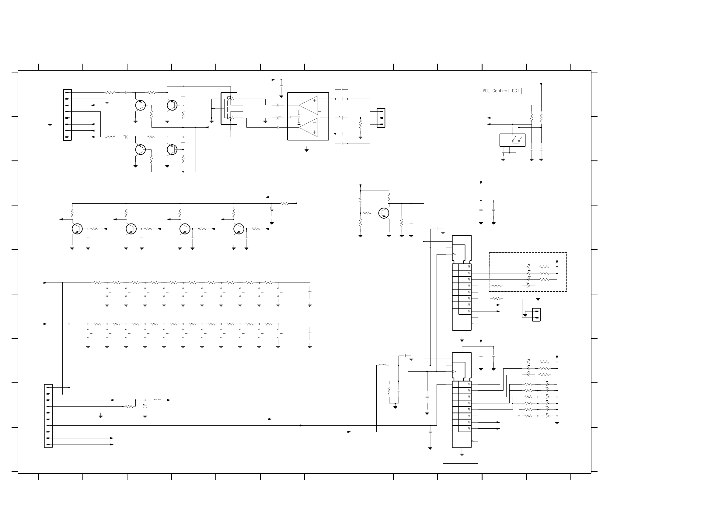
CONTROL BOARD - CIRCUIT DIAGRAM
5-4 5-4
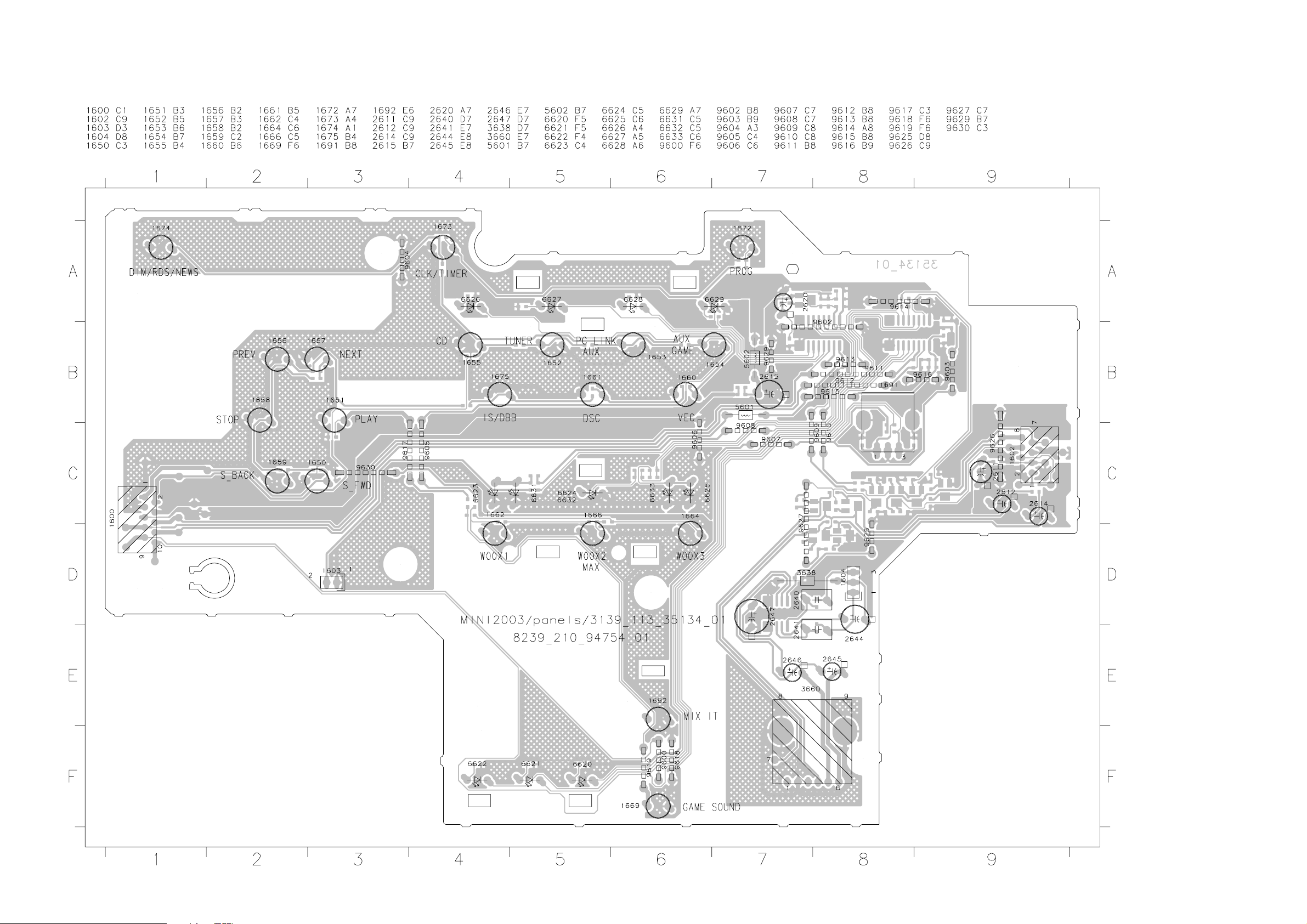
123456789101112
CONTROL
1602
A
1
2
3
4
5
GND_A
6
7
8
B
FE-ST-VK-N
C
4K7
3709
EN22
D
7602
BC847B
GND_A
100p
GND_A
E
KEY1
KEY1
F
KEY2
KEY2
1650
GND_B
G
From Front Display Board
FE-ST-VK-N
H
1600
1
2
3
4
5
6
7
8
9
10
I
# : Provision
Note : Some values may varies, see respective parts list for correct value.
3651
1K
GND_A
+12V_A
EN11
A22
3652
A11
1K
EN11 A22 A11
3653
EN2 E N1 A2 A1
47K
2633
BC847B
GND_A
3663
150R
1655
3664
220R
CD
GND_B
3674
150R
3675
220R
1659
NEXT
PREV
GND_B
GND_B
Gnd
VOL_A
VOL_B
2612
4u7
BC817-25
GND_A
2614
4u7
BC817-25
7608
7610
3685
2K2
3686
2K2
1K
1K
BC817-25
3629
GND_A
BC817-25
3684
7607
7609
1K
820p
820p
1K
2637
3628
2638
3683
2
GND_A
EN22
GND_A GND_A
4K7
3657
100p
3637
47K
2634
7603
GND_A GND_A GND_A
3665
270R
1652
TUNER
GND_B
3676
270R
1658
STOP
GND_B
4600
3636
470R
1653
GND_B
1657
GND_B
# 2615
3666
390R
PC LINK/GAME
GND_B
3677
390R
S_fwd
GND_B
5602
2u2
16V100u
1654
1656
7604
BC847B
GND_A
3667
560R
AUX/GAME
3678
560R
S_back
+5V6
3658
1669
1675
GND_B
4K7
3655
47K
2635
100p
MIX IT
IS/DBB
3669
1K2
1662
WOOX1
1661
GND_B
3680
1K2
DSC
GND_BGND_B
3668
820R
3679
820R
GND_BGND_B
Gnd
3660
8
9
EWCY8AF20A24
7605
BC847B
GND_A
3670
1K8
1666
WOOX2/MAX
3708
1K8
1660
VEC
7
6
1
3
5
GND_A
20K
4
+12V_A_B
4K7
3659
3656
47K
100p
2636
3671
2K7
1664
WOOX3
GND_B
GND_B
3681
2K7
1674
DIM/RDS/NEWS
GND_B GND_B
+12V_A_B
GND_A
1692
1673
3672
4K7
GAME SOUND
3682
4K7
CLK/TIMER
LEDShClk
GND_A
2645
2u2 50V
2647
47u 35V
2646
2u2 50V
2611
1651
GND_B
GND_B
16V22u
1672
100n
3647
470R
2648
7
4
6
PLAY
PROG
OUTL
SVRR
OUTR
VCC
GND_A
GND
+12V_A
8
VCC
5
2623
GND_B
2624
GND_B
ShData
7620
TDA8579T
INL+
IN-
INR+
100p
100p
1600 H1
1602 A1
1603 F12
1604 B8
A
B
C
D
E
F
G
H
1650 F2
1651 E6
1652 E2
1653 E3
1654 F3
1655 F2
1656 F3
1657 F3
1658 F2
1659 F2
1660 F5
1661 F4
1662 E4
1664 F5
1666 F5
1669 E4
1672 F6
1673 F5
1674 F5
1675 F4
1691 B11
1692 E5
2611 D6
2612 A2
2614 B2
2615 H3
2616 D9
2617 G9
2620 C8
2621 B12
2622 B12
2623 E7
2624 F7
2625 D10
2626 D11
2627 D9
2628 G10
2629 G11
2630 I9
2631 H9
2632 H9
2633 D2
2634 D3
2635 D4
2636 D5
2637 A4
2638 B4
2640 A7
2641 B7
2642 A7
2643 B7
2644 A7
2645 A6
2646 B6
2647 A6
2648 A6
3628 A4
3629 A3
3630 H11
3636 H3
3637 D3
3638 B8
3647 C6
3651 A2
3652 B2
3653 D2
3655 D4
3656 D5
3657 D2
3658 D4
3659 D5
3660 A5
3661 B12
3662 B12
3663 E2
3664 E2
3665 E3
3666 E3
3667 E4
3668 E4
3669 E4
3670 E5
3671 E5
3672 E6
3674 F2
3675 F2
3676 F3
3677 F3
3678 F4
3679 F4
3680 F4
3681 F5
3682 F6
3683 B4
3684 B3
3685 A3
3686 B3
3689 C8
I
3690 D8
3691 D8
3692 D9
3695 H8
3696 E12
3697 E12
Gnd
2621
Gnd
3661
6626
6627
6628
1
2
1603
+5V6
10K
10K
3662
10n
10n
2622
Gnd
+5V6
3696
470R
470R
3697
3698
470R
AUX
Gnd
HR
USB LED
# 2640
220n
2642
1
220n
2644
2
22u35V
2643
3
220n
# 2641
220n
GND_A
100R
3638
HR
3
2
1
1604
VOL_A
VOL_B
1691
EC12
1A3
B
C
2
4
5
Gnd
+5V6
2620
3691
Gnd
10u
3690
10K
10K
7650
BC847B
3689
Gnd
4K7
1n
10K
3692
Gnd
2627
Gnd
2616
7606
74HC4094D
1n
Gnd
SRG8
15
EN1
1
STB
3
2
D1
+5V6
1n
2626
1n
2625
GndGnd
16
NOT FOR ALL VERSION
4
5
6
3699
7
470R
CD
TUNER
PC_LINK
6629
14
13
12
11
270R3701
EN2
EN1
9
10
8
+5V6
SRG8
15
EN1
1
STB
3
2
D1
Gnd
16
100n
2628
2629
100n
6621
6622
3705 220R
220R3710
220R3630
220R
3711
220R3706
3712
220R
6620
Gnd
4
5
6
7
13
12
11
Gnd
14
A2
A1
6623
6631
6624
6632
6625
6633
3702
3703
3704
Gnd
+5V6
180R
180R
180R
GAME_SOUND_2
GAME_SOUND_1
GAME_SOUND_3
WOOX_1
MAX
WOOX_2
MAX
WOOX_3
MAX
9
LEDShStr
5601
2u2
3695
10K
Gnd
2632
2617
1n
220p
Gnd
2631
Gnd
2630
220p
1n
7601
74HC4094D
10
Gnd
8
Gnd
3139 118 56720...8239_210_94754 for 3513 pt4 dd wk0310
3698 E12
3699 E11
3701 F11
3702 G12
3703 G12
3704 G12
3705 G11
3706 H11
3708 F5
3709 D1
3710 H11
3711 H11
3712 H11
4600 H3
5601 G8
5602 H3
6620 G12
6621 G12
6622 G12
6623 H12
6624 H12
6625 H12
6626 E12
6627 E12
6628 E12
6629 E11
6631 H12
6632 H12
6633 H12
7601 G10
7602 D1
7603 D2
7604 D4
7605 D5
7606 D10
7607 A3
7608 A3
7609 B3
7610 B3
7620 A7
7650 C8
123456789101112
5-5
5-5
ECO POWER BOARD - COMPONENT LAYOUT
This assembly drawing shows a summary of all possible versions. For components
used in a specific version see schematic diagram and respective parts list.
3139 113 3513 pt4 dd wk0310
ECO POWER BOARD - CIRCUIT DIAGRAM
ECO POWER BOARD - CHIP LAYOUT
This assembly drawing shows a summary of all possible versions. For components
used in a specific version see schematic diagram and respective parts list.
3139 113 3513 pt4 dd wk0310
GAME PORT BOARD - COMPONENT LAYOUT
This assembly drawing shows a summary of all possible versions.
For components used in a specific version see schematic diagram
and respective parts list.
GAME PORT BOARD - CHIP LAYOUT
This assembly drawing shows a summary of all possible versions.
For components used in a specific version see schematic diagram
and respective parts list.
1880 A1 1881 B2 2880 A2 3880 B2 3881 A3
123
ECO POWER
FE-ST-VK-N
1880
A
+5V6
+L
Gnd_supply
Key0
Gnd_key
1
2
3
4
5
1881
B
6880
1N4148
3880
6880 A2 6881 B2 7880 B3
4u7
3881
2880
820R
BC857B
7880
47K
6881
A
B
3139 113 3513 pt4 dd wk0310
GAME PORT BOARD - CIRCUIT DIAGRAM
1890 A3
1891 B4
1892 B3
1893 A1
1894 C1
1897 A4
2890 C4
2891 B2
2892 B3
2894 A2
2895 A3
2896 B4
1234
GAME PORT
A
EH-S
1893
1
2
3
3891
10K
3890
10K
B
2
1
HR 1894
C
2894
2891
2897 B4
3890 A2
3892
1K2
680p
3893
1K2
680p
2895
2892
3891 A2
3892 A3
470p
470p
3893 B3
1890
YKC21-3826
2
1
2
1
1892
YKC21-3564
2
1
GND_video
3139 113 3513 pt4 dd wk0310
1897
3
1891
100p
3
YKC21-4503N
2890
3
RT-01T1
2896
220n
100p
A
2897
B
C
Note : Some values may varies, see respective parts list for correct value.
123
3139 118 56720...8239_210_94794 for 3513 pt4 dd wk0310
Note : Some values may varies, see respective parts list for correct value.
1234
3139 118 56720...8239_210_94824 for 3513 pt4 dd wk0310

5-6 5-6
VU METER (LEFT) BOARD - COMPONENT LAYOUT
This assembly drawing shows a summary of all possible versions. For
components used in a specific version see schematic diagram and respective
3139 113 3513 pt4 dd wk0310
VU METER (LEFT) BOARD - CHIP LAYOUT
parts list.
VU METER (LEFT) BOARD - CIRCUIT DIAGRAM
1810 C1
1811 D4
2810 D2
2811 D3
2812 C2
2813 A2
2814 D3
3811 C2
3812 D2
3813 D3
3814 D3
3815 C2
3816 B3
3817 B2
3818 B3
3819 B2
3820 B3
3821 A3
1234
VU METER (LEFT)
A
B
To Front Display Board
C
1810
HR
1
VUMeter
2
3
D
+5V6
Vu_cntl
2813
Gnd
3824
220R
2812
Gnd
3811
4K7
16V
47u
35V
4u7
Gnd
2810
100p
+5V6
7811
BC847B
470R
470R
470R
3812
3820
1K2
3819
3818
4K7
3817
3816
1K2
3815
7810
BC847B
3813
100K
1K
2811
3822 A3
3823 A4
3824 A2
6812
Gnd
Vu_cntl
2814
4u7 25V
3821
3814
8K2
6812 A3
6813 A3
6814 A4
330R
7812
BC847B
4u7 25V
6815 D3
7810 C2
7811 A2
3822
330R
6813
7813
BC847B
Gnd
Gnd
+5V6
To VU Meter Housing (Left) Board
6815
1N4148
3823
6814
7812 B3
7813 B4
7814 B4
330R
7814
BC847B
1811
1
2
EH-S
A
B
C
D
This assembly drawing shows a summary of all possible versions. For
components used in a specific version see schematic diagram and respective
parts list.
3139 113 3513 pt4 dd wk0310
Note : Some values may varies, see respective parts list for correct value.
3139 118 56720...8239_210_94814 for 3513 pt4 dd wk0310
1234
VU METER HOUSING (LEFT) BOARD - COMPONENT LAYOUT & CIRCUIT DIAGRAM
5900 A2
12
VU METER HOUSING (LEFT)
To VU Meter (Left) Board
5900
AA
12
Vu_Gnd Vu_signal
3139 113 3513 pt4 dd wk0310
3139 118 56720...8239_210_94854 for 3513 pt4 dd wk0310
P-66SI
12
5-7
5-7
VU METER (RIGHT) BOARD - COMPONENT LAYOUT
This assembly drawing shows a summary of all possible versions. For
components used in a specific version see schematic diagram and respective
3139 113 3513 pt4 dd wk0310
VU METER (RIGHT) BOARD - CHIP LAYOUT
parts list.
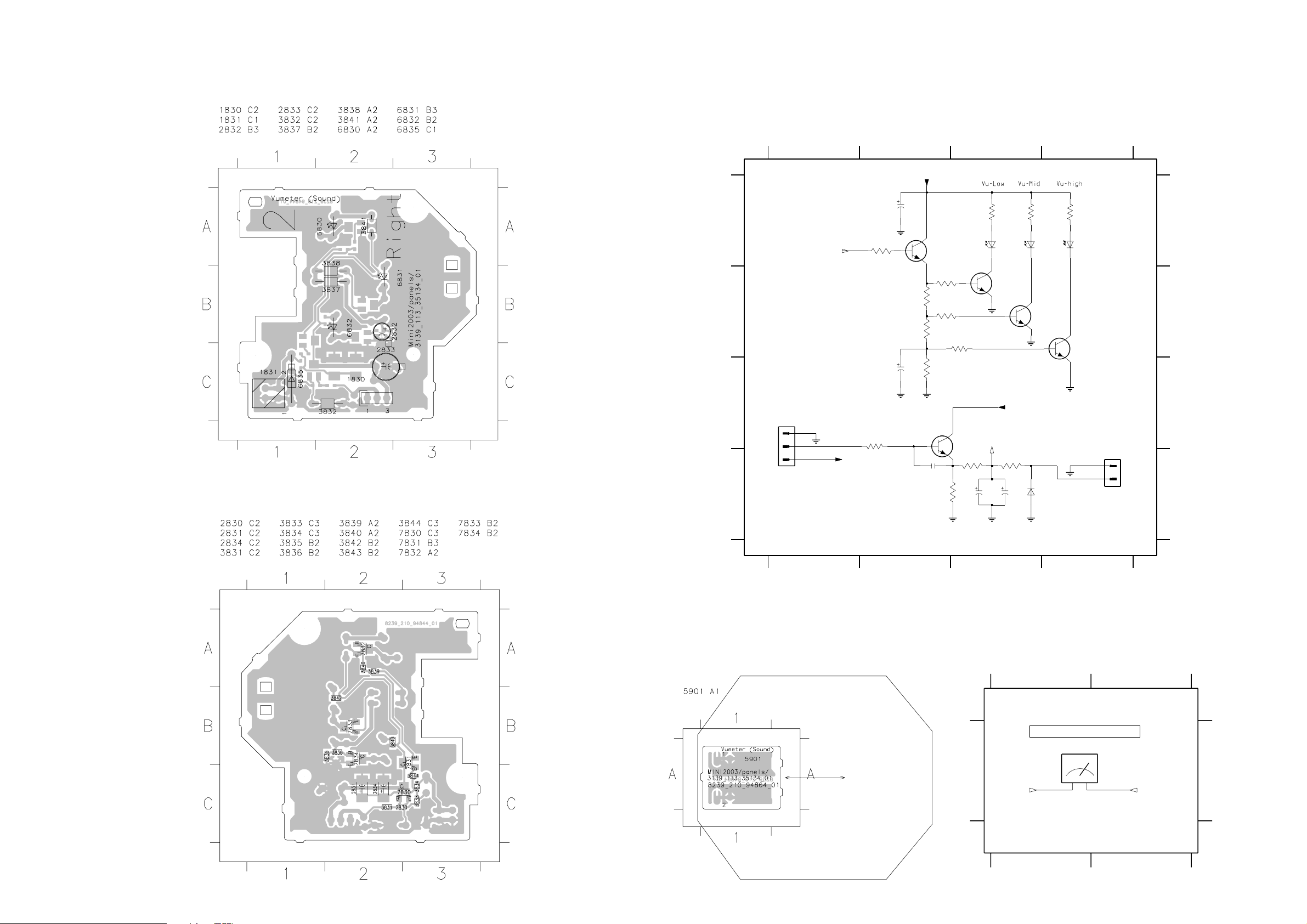
VU METER (RIGHT) BOARD - CIRCUIT DIAGRAM
1830 C1
1831 D4
2830 D2
2831 D3
2832 C2
2833 A2
2834 D3
3831 C2
3832 D2
3833 D3
3834 D3
3835 C2
3836 B3
3837 B2
3838 B2
3839 B2
3840 B2
3841 A3
3842 A3
3843 A4
3844 A2
1234
VU METER (RIGHT)
+5V6
16V
2833
A
B
C
D
To Front Display Board
1830
HR
1
2
3
Vu_cntl
VUMeter
+5V6
3831
4K7
3844
220R
Gnd
Gnd
2832
35V 47u
4u7
Gnd
7831
BC847B
470R
470R
470R
2830
100p
3840
1K2
3839
3838
4K7
3837
3835
3836
1K2
3832
7830
BC847B
3833
100K
1K
Gnd
2831
6830
3841
7832
BC847B
Vu_cntl
4u7
6830 A3
6831 A3
6832 A4
330R
+5V6
3834
8K2
2834
Gnd
25V4u7
3842
6831
6835
6835 D3
7830 C3
7831 A2
7832 B3
7833 B3
7834 B4
3843
330R
7833
BC847B
1N4148
330R
6832
7834
BC847B
Gnd
To VU Meter Housing (Right) Board
1
2
1831
EH-S
A
B
C
D
This assembly drawing shows a summary of all possible versions. For
components used in a specific version see schematic diagram and respective
parts list.
3139 113 3513 pt4 dd wk0310
Note : Some values may varies, see respective parts list for correct value.
3139 118 56720...8239_210_94844 for 3513 pt4 dd wk0310
1234
VU METER HOUSING (RIGHT) BOARD - COMPONENT LAYOUT & CIRCUIT DIAGRAM
5901 A2
12
VU METER HOUSING (RIGHT)
To VU Meter (Right) Board
5901
AA
12
Vu_Gnd Vu_signal
3139 113 3513 pt4 dd wk0310
3139 118 56720...8239_210_94864 for 3513 pt4 dd wk0310
P-66SI
12
5-8 5-8
IR EYE BOARD - COMPONENT LAYOUT IR EYE BOARD - CHIP LAYOUT
This assembly drawing shows a summary of all possible versions. For components
used in a specific version see schematic diagram and respective parts list.
3139 113 3513 pt4 dd wk0310
This assembly drawing shows a summary of all possible versions. For components
used in a specific version see schematic diagram and respective parts list.
3139 113 3513 pt4 dd wk0310
IR EYE BOARD - CIRCUIT DIAGRAM
USB LED BOARD - COMPONENT LAYOUT USB LED BOARD - CHIP LAYOUT
This assembly drawing shows a summary of all
possible versions. For components used in a
specific version see schematic diagram and
respective
parts list.
3139 113 3513 pt4 dd wk0310
This assembly drawing shows a summary of all
possible versions. For components used in a
specific version see schematic diagram and
3139 113 3513 pt4 dd wk0310
respective
parts list.
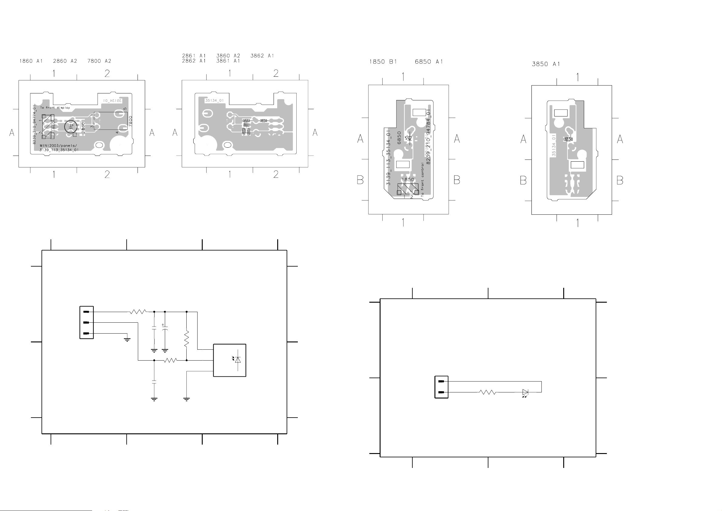
1860 A1 2860 A2 2861 B2 2862 A2 3860 A2
123
IR EYE
1860
A
1
2
3
EH-B
Gnd
100R
3860
Gnd
B
1K
3861
2861
47u
Gnd
2860
47n
2862
2n2
Gnd Gnd
3861 B2 3862 A2 7800 A3
7800
10K
3862
TSOP4836ZC1
VS
OUT
GND
2
GND
A
B
USB LED BOARD - CIRCUIT DIAGRAM
1850 A1 3850 B1 6850 B2
12
USB LED
A
1850
1
2
EH-B
3850
820R
A
LTL-8166FTNN
6850
Note : Some values may varies, see respective
parts list for correct value.
123
3139 118 56720...8239_210_94774 for 3513 pt4 dd wk0310
B
Note : Some values may varies, see respective
parts list for correct value.
B
3139 118 56720...8239_210_94784 for 3513 pt4 dd wk0310
12
 Loading...