


Service Manual
Service
Service
Mini System
Service
Service
Service
FW-C255/21/30/37
TABLE OF CONTENTS
Page
Location of pc boards & Version variations................1-2
Technical Specifications .............................................1-3
Measurement setup....................................................1-4
Service Aids, Safety Instruction, etc. ..........................1-5
Disassembly Instructions & Service positions .............. 2
Service Test Programs & DEMO mode.........................3
Set Block diagram ......................................................... 4
Set Wiring diagram ........................................................ 5
Front Board.................................................................... 6
Mains Board...................................................................8
ECO-MTF Module..........................................................9
3CDC-LC-MB Module..................................................10
Combi Board................................................................ 11
Set Mechanical Exploded view & parts list .................12
COMPACT
DIGITAL AUDIO
CLASS 1
©
Copyright 2002 Philips Consumer Electronics B.V. Eindhoven, The Netherlands
All rights reserved. No part of this publication may be reproduced, stored in a retrieval system or
transmitted, in any form or by any means, electronic, mechanical, photocopying, or otherwise
without the prior permission of Philips.
Published by KC 0201 Service Audio Printed in The Netherlands Subject to modification
Version 1.0
LASER PRODUCT
GB
3139 785 30021
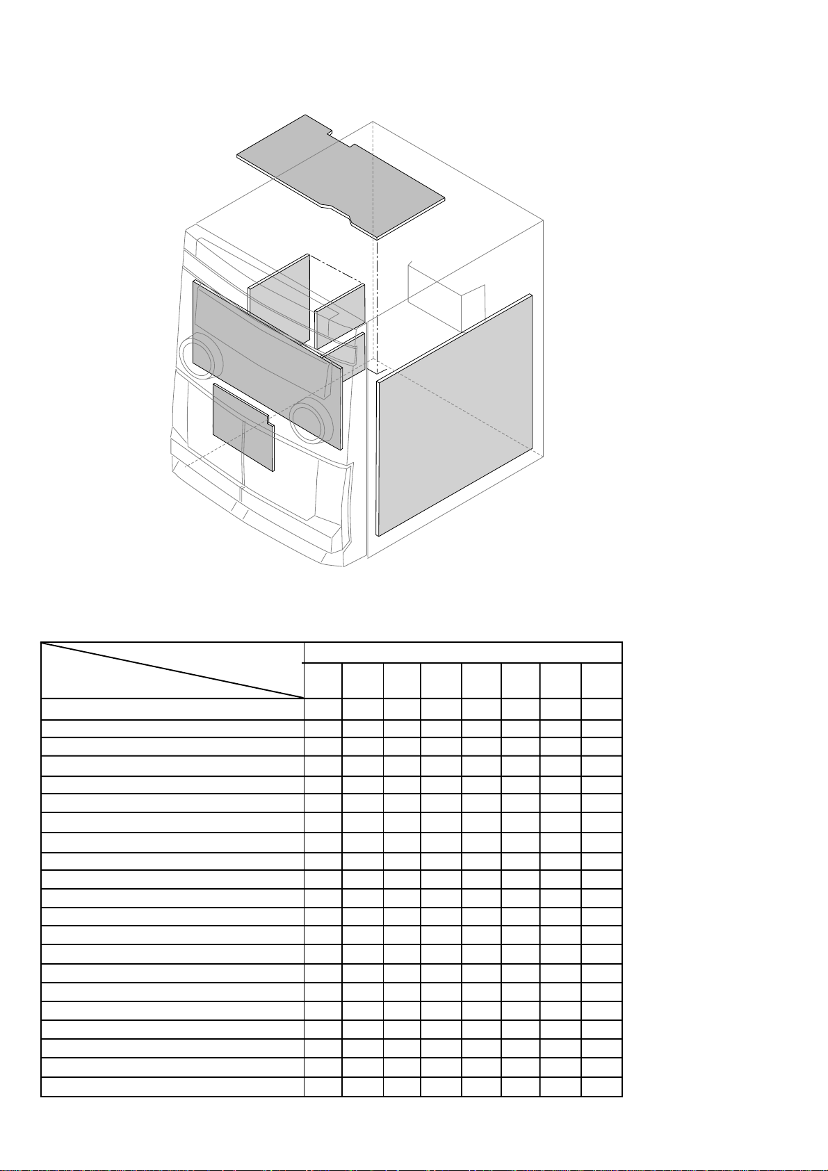
LOCATION OF PC BOARDS
FRONT
BOARD
MAINS
BOARD
(/21/22 O
MTF
BOARD
1-2
CD BOARD
nly)
TRAFO
SEC.
BOARD
TRAFO
PRI.
BOARD
COMBI BOARD
VERSION VARIATIONS:
Type /Versions: FW-C255
Features &
/21 /21M /30 /33 /37
Board in used:
Karaoke x x x
News
RDS
Incredible Surround
Rotary Encoder (volume control) x x x x x
Jog Shuttle x x x x x
Voltage Selector x x
Aux Input x x x x x
Digital Output
Headphone Socket x x x x x
Line Output
Subwoofer Output
Surround Output
Matrix Surround Loudspeakers
Standby - FTD Clock Display x x x x x
ECO Standby - Dark
Combi - Non-Cenelec Tuner x x x x x
Combi - Cenelec Tuner

SPECIFICATIONS
GENERAL:
Mains voltage : 110-127V/220-240V Switchable for /21/21M
120V for /37
230-240V for /30
Mains frequency : 50/60Hz
Power consumption : < 70W Active
< 15W at Standby /37
< 20W at Standby /21/21M/30
Clock accuracy : < 4 seconds per day
Dimension centre unit : 265 x 310 x 365mm
TUNER:
FM
Tuning range : 87.5-108MHz
Grid : 50kHz
100kHz for /21/21M/37
IF frequency : 10.7MHz ± 20kHz
Aerial input : 75Ω coaxial
300Ω click fit for /37
Sensitivity at 26dB S/N : < 7µV
Selectivity at 600kHz bandwidth : > 25dB
IF rejection : > 60dB
Image rejection : > 25dB
Distortion at RF=1mV, dev. 75kHz : < 3%
-3dB Limiting point : < 8µV
Crosstalk at RF=1mV, dev. 40kHz : > 18dB
1-3
CASSETTE RECORDER:
Number of track : 2 x 2 stereo
Tape speed : 4.76 cm/sec +2.5/-1.5%
Wow and flutter : < 0.35% DIN
Fast-wind/rewind time C60 : 130 sec
Bias system : 75kHz ± 5kHz
Rec/Pb frequency response within 8dB : 80Hz - 12.5kHz
Signal to noise ratio Type I : > 48dBA
COMPACT DISC:
Measurement done at output conn. of the CDC module.
Frequency response within ± 1.5dB: 20Hz - 20kHz
Output level (in Vrms) :550mV ± 2dB, R
Signal/Noise ratio (A-weighted) : > 80dBA
Distortion at 1kHz : < 0.003%
Channel unbalance at 1kHz : ±1dB
Channel separation at 1kHz : > 60dB
De-emphasis : 0 or 15/50 mS (Switched by subcode
on the disc)
{....} Values for /21/21M only
1)
6Ω, 1kHz, 10% THD
2)
6Ω, 60Hz-12.5kHz, 10% THD
3)
Frequency response in each setting is software controlled.
= 100Ω
out
MW
Tuning range : 531-1602kHz
530-1700kHz for /21/21M/37
Grid : 9kHz
10kHz for /21/21M/37
IF frequency : 450kHz ± 1kHz
Aerial input : Frame aerial
Sensitivity at 26dB S/N : < 4.4mV/M
Selectivity at 18kHz bandwidth : > 18dB
IF rejection : > 45dB
Image rejection : > 28dB
Distortion at RF=50mV, m=80% : < 5%
AMPLIFIER:
Output power : 2 x 40W
2 x 33W
1)
RMS /21/21M/30
2)
FTC /37
Frequency response within -3dB : 50Hz-15kHz
Dynamic Bass Boost : DBB ON, DBB 1, DBB 2, DBB 3
Digital Sound Control : Jazz, Techno, Optimal, Rock
3)
Headphone output at 32Ω : 15mW ± 2dB
Input sensitivity, R
= 600Ω
S
Aux / CDR : 500mV / 1.0V
Mic : {3.5mV}
3)
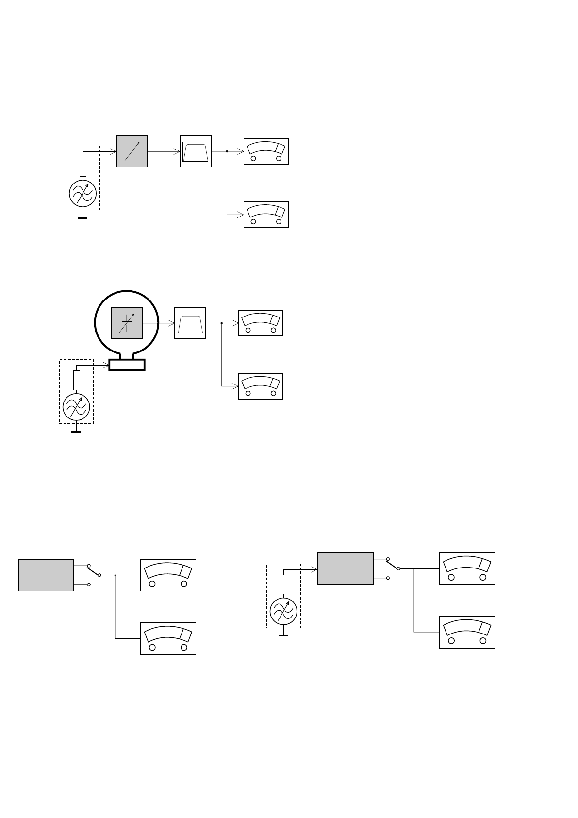
MEASUREMENT SETUP
Tuner FM
1-4
Bandpass
LF Voltmeter
e.g. PM2534
RF Generator
e.g. PM5326
DUT
250Hz-15kHz
e.g. 7122 707 48001
Ri=50Ω
S/N and distortion meter
e.g. Sound Technology ST1700B
Use a bandpass filter to eliminate hum (50Hz, 100Hz) and disturbance from the pilottone (19kHz, 38kHz).
Tuner AM (MW,LW)
RF Generator
e.g. PM5326
Ri=50Ω
DUT
Frame aerial
e.g. 7122 707 89001
Bandpass
250Hz-15kHz
e.g. 7122 707 48001
LF Voltmeter
e.g. PM2534
S/N and distortion meter
e.g. Sound Technology ST1700B
To avoid atmospheric interference all AM-measurements have to be carried out in a Faraday´s cage.
Use a bandpass filter (or at least a high pass filter with 250Hz) to eliminate hum (50Hz, 100Hz).
CD
Use Audio Signal Disc
(replaces test disc 3)
DUT
L
R
SBC429 4822 397 30184
S/N and distortion meter
e.g. Sound Technology ST1700B
LEVEL METER
e.g. Sennheiser UPM550
with FF-filter
Recorder
Use Universal Test Cassette CrO2 SBC419 4822 397 30069
or Universal Test Cassette Fe SBC420 4822 397 30071
LF Generator
e.g. PM5110
DUT
L
R
S/N and distortion meter
e.g. Sound Technology ST1700B
LEVEL METER
e.g. Sennheiser UPM550
with FF-filter
SERVICE AIDS
1-5
Service Tools:
Universal Torx driver holder .................................. 4822 395 91019
Torx bit T10 150mm ............................................. 4822 395 50456
Torx driver set T6 - T20......................................... 4822 395 50145
Torx driver T10 extended ...................................... 4822 395 50423
Cassette:
SBC419 Test cassette CrO2................................. 4822 397 30069
SBC420 Test cassette Fe ..................................... 4822 397 30071
MTT150 Dolby level 200nWb/M............................ 4822 397 30271
Compact Disc:
SBC426/426A Test disc 5 + 5A ............................ 4822 397 30096
SBC442 Audio Burn-in Test disc 1kHz ................. 4822 397 30155
SBC429 Audio Signals disc .................................. 4822 397 30184
Dolby Pro-logic Test Disc...................................... 4822 395 10216
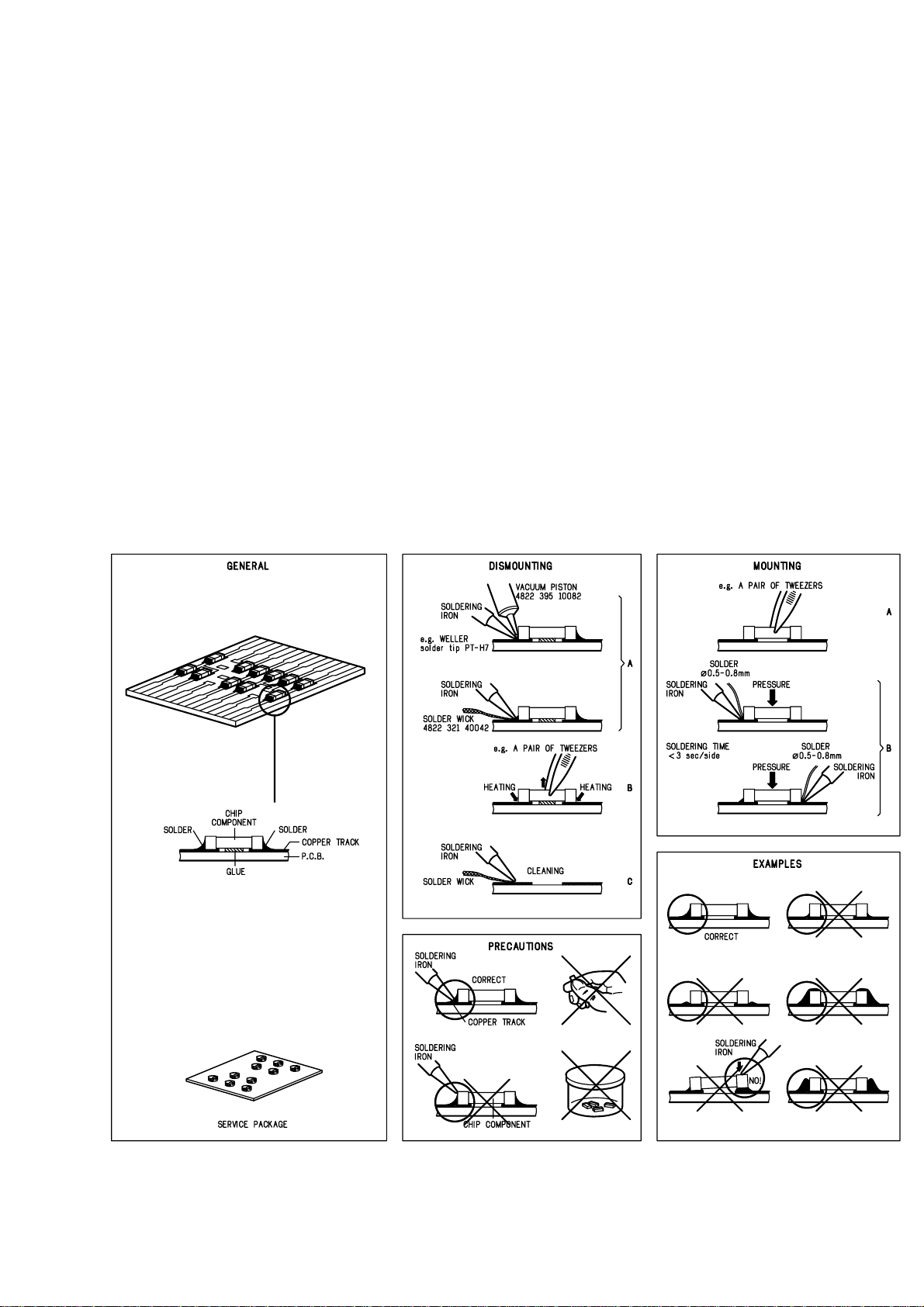
HANDLING CHIP COMPONENTS
ESD Equipment:
Anti-static table mat - large 1200x650x1.25mm ... 4822 466 10953
Anti-static table mat - small 600x650x1.25mm..... 4822 466 10958
Anti-static wristband .............................................. 4822 395 10223
Connector box (1MΩ)............................................ 4822 320 11307
Extension cable
(to connect wristband to conn. box).................. 4822 320 11305
Connecting cable
(to connect table mat to conn. box) .................. 4822 320 11306
Earth cable (to connect product to mat or box) .... 4822 320 11308
Complete kit ESD3
(combining all above products)......................... 4822 320 10671
Wristband tester .................................................... 4822 344 13999
WARNING
GB
All ICs and many other semi-conductors are
susceptible to electrostatic discharges (ESD).
Careless handling during repair can reduce life
drastically.
When repairing, make sure that you are
connected with the same potential as the mass
of the set via a wrist wrap with resistance.
Keep components and tools also at this
potential.
F
ATTENTION
Tous les IC et beaucoup d’autres
semi-conducteurs sont sensibles aux
décharges statiques (ESD).
Leur longévité pourrait être considérablement
écourtée par le fait qu’aucune précaution n’est
prise à leur manipulation.
Lors de réparations, s’assurer de bien être relié
au même potentiel que la masse de l’appareil et
enfiler le bracelet serti d’une résistance de
sécurité.
Veiller à ce que les composants ainsi que les
outils que l’on utilise soient également à ce
potentiel.
1-6
ESD
D
WARNUNG
Alle ICs und viele andere Halbleiter sind
empfindlich gegenüber elektrostatischen
Entladungen (ESD).
Unsorgfältige Behandlung im Reparaturfall kan
die Lebensdauer drastisch reduzieren.
Veranlassen Sie, dass Sie im Reparaturfall über
ein Pulsarmband mit Widerstand verbunden
sind mit dem gleichen Potential wie die Masse
des Gerätes.
Bauteile und Hilfsmittel auch auf dieses gleiche
Potential halten.
WAARSCHUWING
NL
Alle IC’s en vele andere halfgeleiders zijn
gevoelig voor electrostatische ontladingen
(ESD).
Onzorgvuldig behandelen tijdens reparatie kan
de levensduur drastisch doen verminderen.
Zorg ervoor dat u tijdens reparatie via een
polsband met weerstand verbonden bent met
hetzelfde potentiaal als de massa van het
apparaat.
Houd componenten en hulpmiddelen ook op
ditzelfde potentiaal.
I
AVVERTIMENTO
Tutti IC e parecchi semi-conduttori sono
sensibili alle scariche statiche (ESD).
La loro longevità potrebbe essere fortemente
ridatta in caso di non osservazione della più
grande cauzione alla loro manipolazione.
Durante le riparazioni occorre quindi essere
collegato allo stesso potenziale che quello della
massa dell’apparecchio tramite un braccialetto
a resistenza.
Assicurarsi che i componenti e anche gli utensili
con quali si lavora siano anche a questo
potenziale.
GB
Safety regulations require that the set be restored to its original
condition and that parts which are identical with those specified,
be used.
NL
Veiligheidsbepalingen vereisen, dat het apparaat bij reparatie in
zijn oorspronkelijke toestand wordt teruggebracht en dat onderdelen,
identiek aan de gespecificeerde, worden toegepast.
F
Les normes de sécurité exigent que l’appareil soit remis à l’état
d’origine et que soient utiliséés les piéces de rechange identiques
à celles spécifiées.
D
Bei jeder Reparatur sind die geltenden Sicherheitsvorschriften zu
beachten. Der Original zustand des Geräts darf nicht verändert werden;
für Reparaturen sind Original-Ersatzteile zu verwenden.
“Pour votre sécurité, ces documents
doivent être utilisés par des spécialistes agréés, seuls habilités à réparer
votre appareil en panne”.
CLASS 1
LASER PRODUCT
GB
Invisible laser radiation when open.
Avoid direct exposure to beam.
Osynlig laserstrålning när apparaten är öppnad och spärren
är urkopplad. Betrakta ej strålen.
Warning !
S
Varning !
3122 110 03420
I
Le norme di sicurezza esigono che l’apparecchio venga rimesso
nelle condizioni originali e che siano utilizzati i pezzi di ricambio
identici a quelli specificati.
"After servicing and before returning set to customer perform a
leakage current measurement test from all exposed metal parts to
earth ground to assure no shock hazard exist. The leakage current
must not exceed 0.5mA."
Varoitus !
SF
Avatussa laitteessa ja suojalukituksen ohitettaessa olet alttiina
näkymättömälle laserisäteilylle. Älä katso säteeseen!
DK Advarse !
Usynlig laserstråling ved åbning når sikkerhedsafbrydere er
ude af funktion. Undgå udsaettelse for stråling.

DISMANTLING INSTRUCTIONS
2-1 2-1
Dismantling the 3CDC Module
1) Loosen the 4 screws, slide Cover top (pos 253) towards
the rear and remove it upwards.
2) Loosen 3 screws slide the Panel right (pos 252) towards
the rear and remove it outwards. Do likewise for the Panel
left (pos 251).
3) Push the gear slowly towards the front as shown in figure
2 until the CDC tray starts to move out of the Front Cabinet
(pos 101). The CDC tray is now disengage and can be
pulled out completely.
4) Remove the Cover Tray (pos 105) as shown in figure 2.
5) Loosen 4 screws A to remove the CDC Module (pos 1 104)
as shown in figure 2.
A
A
A
Turn the Gear towards the Front
till the CDC Tray starts to open
Dismantling of the Front Panel assembly
1) Loosen 2 screws below the Front Panel (pos 101) mounting
it to the Bottom plate (pos 227).
2) Release the 2 catches on the sides of the Front Panel to
separate it from the Bottom plate.
3) Remove the Volume and Jog Rotary knob if the Front
board needs to be dismantled. For Karaoke versions, the
Karaoke knob (pos 133) also need to be removed.
4) Loosen 8 screws B to remove the Front board as shown in
Figure 5.
5) Loosen 6 screws C and eject both cassette doors to
remove the T ape mechanism (pos 1103) as shown in figure
6.
Note: The Cassette door can be removed only after
the removal of the Tape mechanism and buttons.
Figure 1
Dismantling of the Volume & Jog Rotary knobs
1) Cut a piece of packaging tape approximately 5cm width by
12cm length and tape its narrow side on to the top and
bottom side of the Volume knob (pos 132) as shown in
figure 3.
Figure 2
Figure 5
2) Place a small screw driver in between the tape & knob (see
figure 3) to give more leverage in pulling out the knob as
shown in figure 4.
3) Do likewise for the Jog Rotary knob (pos 131). You may
have to rotate the knob to provide the most exposed area
during application of the packaging tape.
Figure 3
Figure 6
Figure 4
Dismantling of the Cassette door Lenses
1) Loosen the Lens Cassette Strip Left Top (pos 163) by
pushing it towards the inside as indicated in Figure 7 and
remove it by using a minus screw driver force it out as
indicated in Figure 8.
Push in this
direction
Push in this
direction
2-2
2) Remove the Lens Cassette Left (pos 161) by pushing it
towards the inside as indicated in Figure 7. Be careful not
to damage or break the catch A.
3) Do likewise for the right Cassette Door Lens (pos 160 and
162).
Use a minus screw
driver to push the Lens
in the direction shown
Catch A
2-2
Service pos A
Figure 7
Dismantling of the Bottom & Rear Panel assembly
1) Loosen 5 screws D mounting the Combi board to the Rear
Panel (pos 254) as shown in figure 9.
2) Loosen 3 screws E and release the 2 catches on the sides
of the Rear Panel to separate it from the Bottom plate (pos
227).
3) Loosen 4 screws G to remove the Mains Transformer.
5) Loosen 2 screws F to remove the Combi Board.
Figure 8
Service pos B
Note: After re-assembly, it is very important to ensure all
wires are routed properly to ensure that they do not
touch/obstruct all moving parts.
The 3CDC Module can be complete detached while
repair the other portion of the set.
Figure 9
Figure 10
3-1
3-1
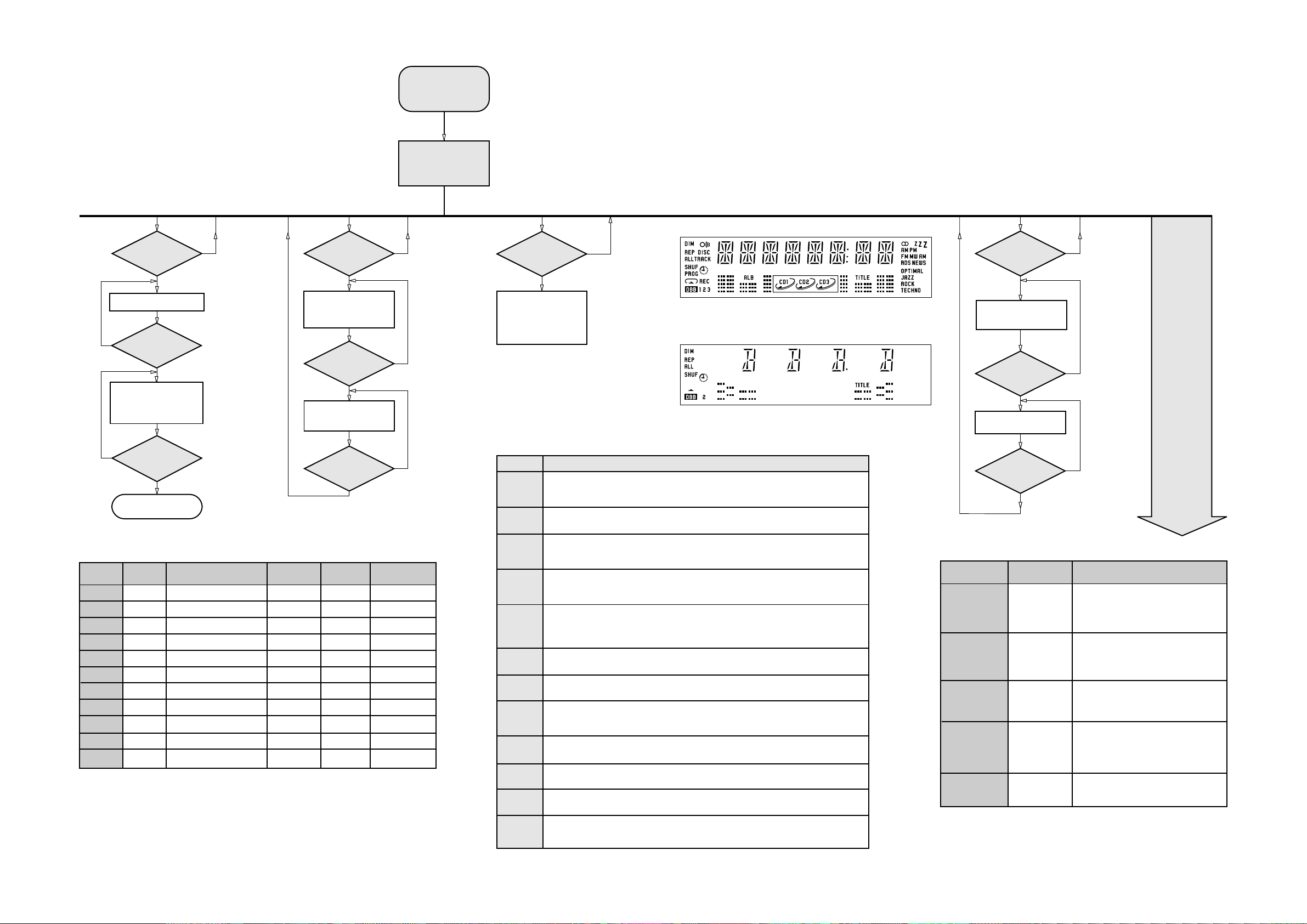
SERVICE TEST PROGRAM
TUNER
TEST
TUNER
Button pressed?
Y
Display Tuner Version
"ccc"
N
copied to the RAM (see Table1)
N
PRESET
1
2
3
4
5
6
7
8
9
10
11
TUNER
Button pressed?
Y
Service frequencies are
Tuner works normally
except:
PROGRAM button
Disconnect
Mains cord ?
Y
Service Mode left
Europe
"EUR"
87.5MHz
108MHz
531kHz
1602kHz
558kHz
1494kHz
87.5MHz
87.5MHz
87.5MHz
87.5MHz
98MHz
Note: * Depending on the selected grid frequency (9 or 10kHz)
By holding the TUNER and R buttons depressed while switching on the Mains supply, one
of the undermentioned features will be activated:
- the tuning grid frequency is toggled between 9kHz and 10kHz for the Oversea (/21) version.
- the extended FM1 (65.81MHz - 74MHz) is toggled on and off for East Eur. (/34) version.
N
East Eur. Extended-band
"EAS"
65.81MHz
108MHz
74MHz
87.5MHz
531kHz
1602kHz
558kHz
1494kHz
98MHz
70.01MHz
65.81MHz
Table 1
To start service test program
plugging in the mains cord
QUARTZ
TEST
O
Button pressed?
Y
Display shows
32K
Output at (Front Board)
pin 80 of uP = 2048Hz
O
Button pressed?
Y
Display shows
8M
Output at (Front Board)
pin 80 of uP = 1,953.125Hz
9
Button pressed?
Y
Note: During the 3CDC tray may "jerks" open
& close or the carousel may rotates
slightly. This is due to sharing of control
lines during the Service test program.
East Eur.
"EAS"
87.5MHz
108MHz
531kHz
1602kHz
558kHz
1494kHz
87.5MHz
87.5MHz
87.5MHz
87.5MHz
98MHz
USA
"USA"
87.5MHz
108MHz
530kHz
1700kHz
560kHz
1500kHz
98MHz
87.5MHz
87.5MHz
87.5MHz
87.5MHz
N
N
N
Oversea
"OSE"
87.5MHz
108MHz
530/531kHz*
1700/1602kHz*
560/558kHz*
1500/1494kHz*
98/87.5MHz*
87.5MHz
87.5MHz
87.5MHz
87.5/98MHz*
hold P & TAPE
depressed while
Display shows the
ROM version *
"S-Vyy"
(Main menu)
S refers to Service Mode.
V refers to Version.
yy refers to Software version number of Processor.
(Counting up from 01 to 99)
SERVICE
PLAY MODE
STANDBY-ON
Button pressed?
Y
Set is in Service PLAY Mode.
In case of failures, error
codes according to table 2
will be displayed.
The Service Play Mode is intended to
detect and identify the failures in the CD Mode.
In this mode the electronics will still function
even when an error is detected so that
repair activities can be carried out.
Error code
E1000
Error Description
Focus Error
Triggered when the focus could not be found within a certain time when starting up the CD
or when the focus is lost for a certain time during play.
E1001
E1002
Radial Error
Triggered when the radial servo is off-track for a certain time during play.
Sledge In Error
The sledge did not reach its inner position (inner-switch is still close) before approximately
6 Sec. have passed by. Inner-switch or sledge motor problem.
E1003
Sledge Out Error
The sledge did not come out of its inner position (inner-switch is still open) before approximately
250 mSec. have passed by. Inner-switch or sledge motor problem.
E1005
Jump-offtrack error
Triggered in normal play when the jump destination could not be found within a certain time.
When this error occurred, software will try to recover by initiating the jump command again.
If it is recoverable, the disc will continue to play.
E1006
E1007
E1008
Subcode Error
Triggered when a new subcode was missing for a certain time during play.
PLL Error
The Phase Lock Loop could not lock within a certain time.
Turntable Motor Error
Generated when the CD could not reached 75% of speed during startup within a certain time.
Discmotor problem.
E1020
E1070
E1071
E1079
Focus Search Error
The focus point has not been found within a certain time.
This happens when the carousel switch is defective and closed all the time, or when the
carousel is blocked when it is located exactly at a disc position.
This happens when the carousel switch is defective and does not closed electrically, or when
the carousel is blocked in between two disc positions. The time-out is approximately 5 Sec.
The drawer could not open or enter the inside position and is opening again. This happen when
the drawer is blocked and cannot go fully inside or when the drawer switch is defective and does
not close.
N
note 1 : JAZZ & TECHNO are on while OPTIMAL is off, other LEDs status
are not important (applicable only for sets with LEDs)
Figure 1
note 2 : OPTIMAL is on while JAZZ & TECHNO are off, other LEDs status
are not important (applicable only for sets with LEDs)
Figure 2
Table 2
Mini 2002 FW-C1xx, C2xx, C3xx Dated: wk141
DISPLAY
TEST
DIM
Button pressed?
Y
Display shows Fig. 1
and selected LEDs on
(see note 1)
DIM
Button pressed?
Y
Display shows Fig. 2
and selected LEDs on
(see note 2)
9
Button pressed?
Y
TEST
Activated with
EEPROM TEST A test pattern will be sent to the EEPROM.
9 to Exit
ROTARY
ENCODER TEST
LEAVE SERVICE
TESTPROGRAM
Volume Knob
Jog Shuttle knob
Disconnect
mains cord
N
N
N
Various
other Tests
ACTION
R
QEEPROM FORMAT Load default data. Display shows "NEW"
or
DBBDEMO
"PASS" is displayed if the uProcessor read
back the test pattern correctly, otherwise
"FAIL" will be displayed.
for 1 second.
Caution!
All presets from the customer will be lost!!
Display shows value for 2 seconds.
Values increases or decreases in steps of 1
until 0 (Min.) or 40 (Max.) is reached.
DEMO will toggle on or off.
The message: "DEMO ON" or "DEMO OFF"
will scroll across the display to show the
new status of the set.
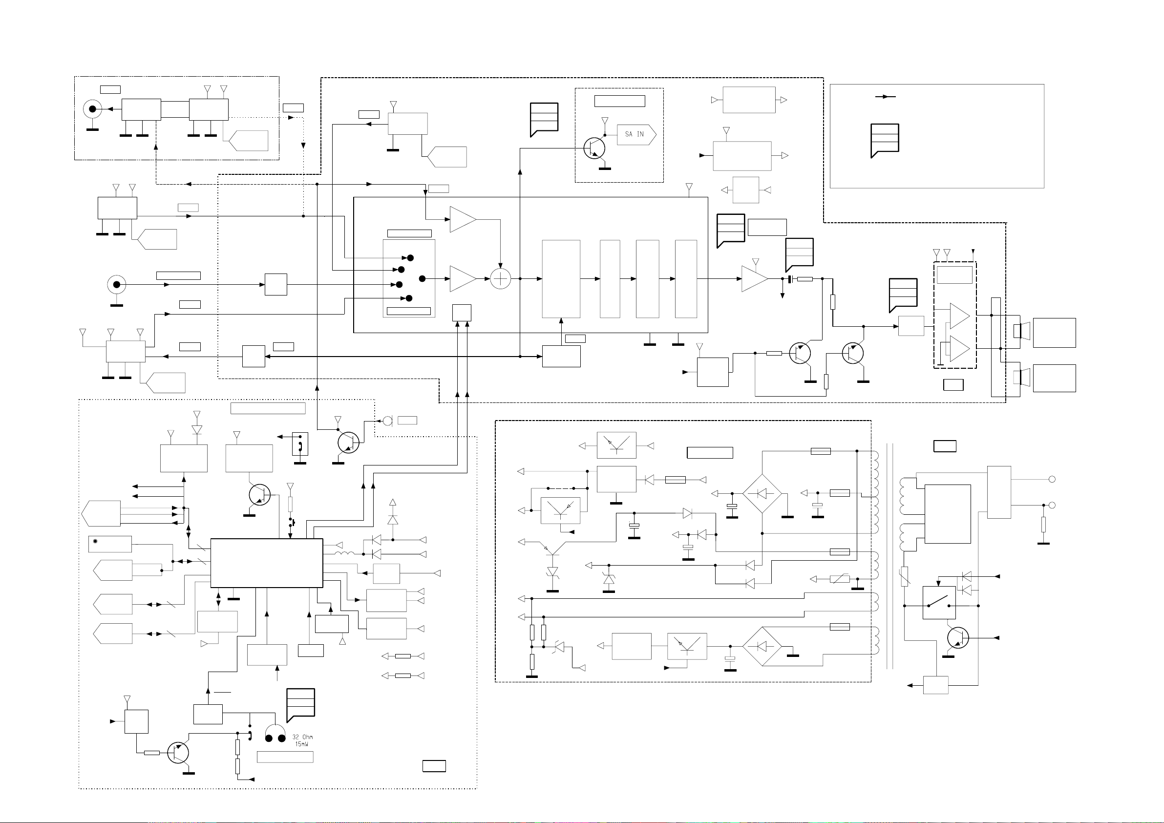
SET BLOCK DIAGRAM
+CD
VDC-3C
M
250mV
120mV
25mV
VIDEO OUT
-6dB Track
-CMOS
250nWb/m
1.0 Vpp
MPEG3
A
D
+CD
+12V_M
3CDC-L2C
DM
AUX / CDR
A
+12V_M +12V_A
ECO-MTF
AM
-6dB Track
# FOR VCD/MP3 VERSION
CDC
CONTROL
500mV / 1000mV
TAPE
CONTROL
+12V_M
D
CDC
CONTROL
ATTN.
-26 dB
ATTN.
-8.5dB
500mV
250mV
4-1
125mV
+12V_A
ECO6
A
SOFTWARE CONTROL
SOURCE SELECTOR
FM (67.5 kHz)
AM (80% MOD)
TUNER
CONTROL
100mV
14 dB
I2C
I2C DATA
I2C CLK
500mV
76dBA
16dB
INCREDIBLE
SURROUND
INTERFACE
500mV
SIMPLE
IS FILTER
SA BUFFER
+12V_A
A
VOL. 1
TREBLE
&
BASS
A
TDA7468
VOL. 2
D
MUTE
CD_ON
+9.1V
-33V
(FOR CDC-L2C ONLY)
+9.1V
LEFT/RIGHT
+5V6
MUTE
+12V_A
CD SUPPLY
CONTROL
500mV
76dBA
16dB
-CMOS (-9V)
REG
+9V
REG
HEADPHONE
AMPLIFIER
+12V_A
NJM4556AM
+12V_A
HP_OUT
-CMOS
+CD
2.50V
85dBA
3dB
(+5V)
1K
4-1
NOTE :
MEASUREMENTS ARE IN AUX MODE :
XX mV
YY dB\A
ZZ dB
# PROVISION FOR VCD/MP3 VERSION
1K
D
D
MAIN SIGNAL PATH
LEVELS AT MAX VOL
S/N AT 500mW\
HEADROOM (1% THD) WRT TO LEVEL AT MAX VOL
1.90V
67dBA
3.0dB
ATTEN.
Rin = 3k
LEFT/RIGHT
+C
+Z
POWER
AMPLIFIER
AN17830A
+
-
+
-
COMBI
AMP_ON
L/R SPEAKER
2 X 37W
2 X 6 OHMS
##
FOR MATRIX
SURROUND
0.9W/6 ohms
POWER
CONTROL
RDS
DECODER
HP_MUTE
CD_ON
AMP_ON
TUNER
CONTROL
CDC
CONTROL
TAPE
CONTROL
+5V6
NTC
PWDN
LPC
MUTE
+5V6_ECO
+LPS
ECO POWER
LED
+F
HP DET
SIMPLE KARAOKE
+5V6
4 X DSC LEDS
D
EEPROM
HP DET
MIC DET
D
uP
TMP87CS71F
KEY SCAN
MATRIX
MIC DET
+LPS
SWITCH
A
ECO/SLEEP
650mV
78dBA
3.2dB
POWER
SWITCH
SA IN
+12V_A
A
I2C DATA
JOG
CONTROL
## FEATURE PROVISION
3.5mV
+5V6
+12A
I2C CLK
+F
+12M
-33V
IR EYE
FTD
VOLUME
CONTROL
+F
F1x
F2x
+5V6
+5V6_ECO
+LPS
F1x
F2x
+F
F1
F2
-33V
F1
F2
(ETF7 ONLY)
PWDN
AMP_ON
+CD
(+5V)
-33V
REGULATOR
7812
# VCD
REGULATOR
L7805
+C
FUSE
FOR CLASS G SWITCH
+50V
CD_ON
POWER SUPPLY
+Z
# VCD
+Z
# VCD
FUSE
FUSE
+C
FUSE
NTC
FUSE
# VCD
# FOR VCD/MP3 VERSION
+5V6_ECO
TRAFO
FOR -/21 ONLY
VOLTAGE
SELECTOR
LPS
SMPS
MAINS
CHOKE
(NOT USED FOR -/37)
(ONLY FOR -/37)
+C
STBY TRANSFORMER
(NOT USED IN -/21 & -/37)
LPC
L
N
10M
FW-C255 Block diagram ...34280 dd wk148
33R
HEADPHONE
47R
A
HP_OUT
FRONT
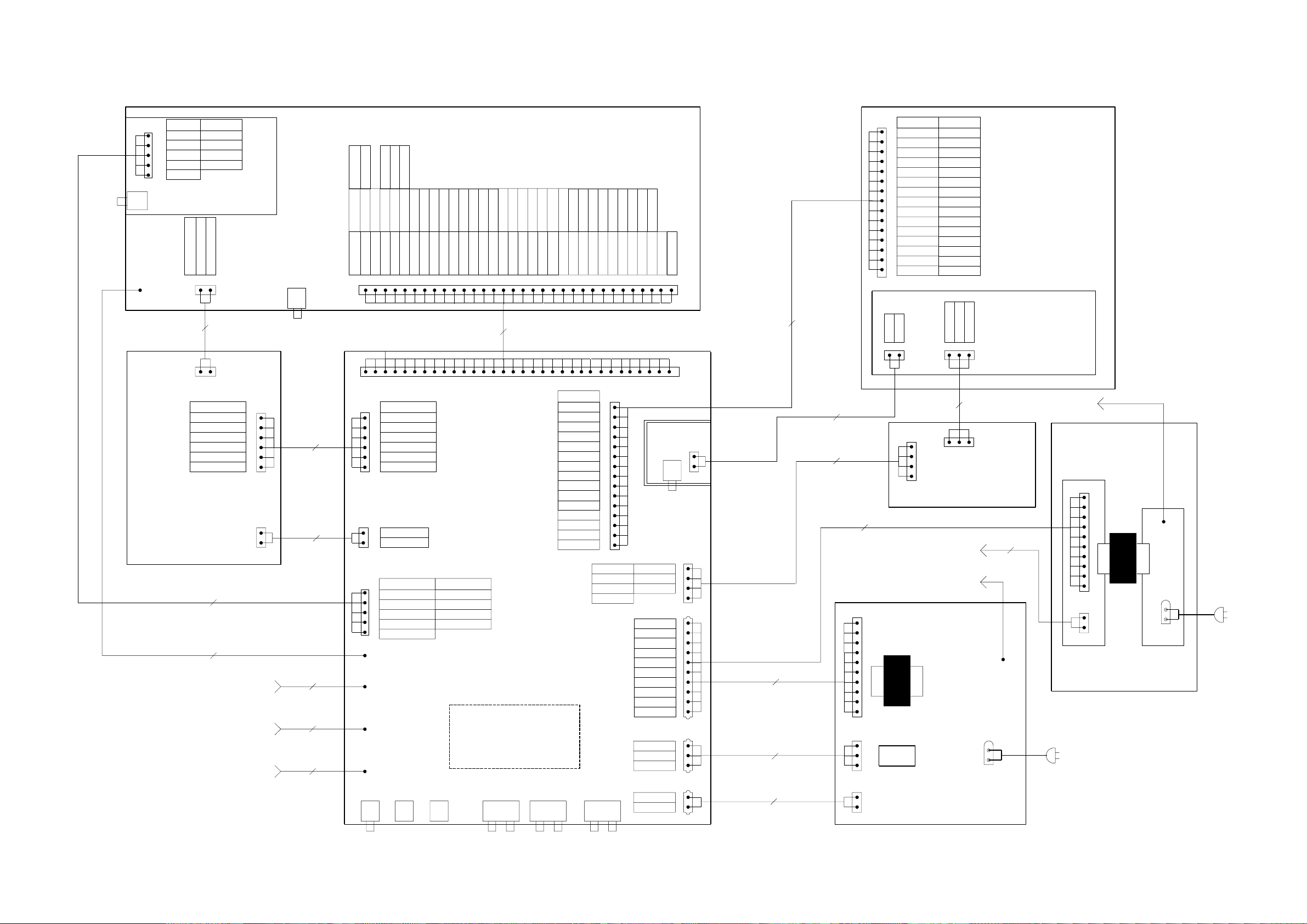
SET WIRING DIAGRAM
5-1 5-1
+12V_A
NON-VCD
MIC_DET
+12V_A
MIC_SK
GND_A
PB INFO
ECO-MTF
REC INFO
1
1401
1401
2P
1706
2
ECO-MTF
TP_REC_LEFT
TP_REC_RIGHT
GND_A
TP_LEFT
+12V_A
TP_RIGHT
EH SIDE
220mm
EH SIDE
1710
1
FFC TOP
1721
1
MIC
1
FFC SIDE
# VCD
MIC_DET
MIC_SK
GND_A
MIC_VCD
MIC AMP
# 1801/1802
1601
ECO-MTF
(1103)
EH TOP
1500
# 5P/4P
FFC AD
140mm
1601
1P
180mm
HEATSINK WIRE
180mm
SOLDERED FROM 8201 or 8203
(UL GROUNDING WIRE - ONLY FOR -/37 VER.)
280mm
FROM ECO-MTF MODULE’S CHASSIS
(BOTTOM SCREW NEAR THE COMBI PCB)
120mm
NOTE :
# - PROVISION FOR SETS WITH VCD/MP3 FEATURE .
## - PROVISION FOR SETS WITH MATRIX SURROUND.
$$ - PROVISION FOR SETS WITH ECO FEATURE (ONLY FOR -/22 VER.) .
HEADPHONE
1700
6P
FFC AD
340mm
1701
2P
340mm
1560
1P
1211
1P
1106
1P
VCD
DSA_STR
$$ 1439
ECO
CD_PORE
1438
CD_PORE
NON-ECO
1
1508
1
1502
FFC TOP
1500
EH TOP
FFC TOP
1560
1568
STOKO PIN
1564
STOKO PIN
1102
FM COAX
(NOT USA) (USA)
DSA_ACK
CD_GND
CD_SILD
CD_GND
CD_SILD
ECO-MTF
1
TP_REC_LEFT
TP_REC_RIGHT
GND_A
TP_LEFT
+12V_A
TP_RIGHT
1
GND_M
+12V_M
#VCD
1
MIC_DET
+12V_A
MIC_SK
GND_A
MIC_VCD
1563
STOKO PIN
FM CLICK
DSA_DATA
CD_SHDATA
CD_SHDATA
# 1505
1101
SH_DATA
CD_SHCLK
CD_SICL
CD_SICL
CD_SHCLK
TU_DATA
TU_CLK
TU_ENABLE
TU_CLK
TU_ENABLE
TU_DATA
1400
TU_STEREO
TU_STEREO
CD_SWINFO
CD_ON
CD_SHSTR
CD_ON
CD_SWINFO
CD_SHSTR
TU_GND
TU_GND
COMBI
(1102)
1503
NON-VCD
MIC_DET
+12V_A
MIC_SK
GND_A
TUNER
ECO6 LAYOUT CELL
1103
AM ANT
1501
AUX IN
D_GND
SA_IN
D_GND
SA_IN
30P / $$ 32P
FFC AD
AMP_ON
HP_RIGHT
HP_GND
HP_LEFT
AMP_ON
HP_GND
HP_RIGHT
HP_LEFT
180mm
1307
LOUDSPEAKER
-33V
MUTEF2F1
F1
-33V
MUTE
F2
CDC-L2C
CD_LEFT 1
GND_A
CD_RIGHT
+5V_CD
GND_M
+12V_M
SW_INFO
SHR_STR
SH_CLK
SICL
SH_DATA
SILD
CD_GND
PORE
GND_D
MIC_VCD
GND_A
MIC_DET
+12V_A
## 1322/1323
MATRIX
SURROUND
FRONT
(1101)
I2C_DATA
D_GND
I2C_CLK
I2C_CLK
D_GND
PWDN
I2C_DATA
PWDN
FFC TOP
MIC_VCD
GND_A
MIC_DET
F1
F2
AC_VKK
GND
NTC
AC_H
AC_H
AC_CT
AC_H
AC_H
PWDN
LPC
5V6_ECO
AC_VCD
AC_VCD
+5V6
+5V6
1507
NTC
NTC
+5V6_ECO
LPC
# VIDEO
# 1506# 1509
EH TOP
1
1
DIPMATE
1
DIPMATE
# 88
1
DIPMATE
FFC SIDE
FFC TOP
1804
EH TOP
86
$$ 87
1805
FFC SIDE
1800
15P
180mm
FFC BD
# 1801
2P
220mm
1
# 1802
3P/4P
220mm
1
CVBS
1
# 1603
CDC-L2C
CD_LEFT
GND_A
CD_RIGHT
+5V_CD
GND_D
+12M
CD_SWINFO
CD_SHSTR
CD_SHCLK
CD_SICL
CD_SHDATA
CD_SILD
GND_D
PORE
GND_D
GND_D
EH SIDE
# 1705
EH TOP
# VCD GROUND ISOLATOR
1210
10P
280mm
1211
1
1210
10P
280mm
TO DIPMATE 88
TO STOKO PIN 1568
LPS-MAINS
VCD
CD_LEFT
GND_A
CD_RIGHT
+5V_CD
GND_D
+12M
CD_SWINFO
CD_SHSTR
CD_SHCLK
SH_DATA
DSA_DATA
DSA_ACK
GND_D
DSA_STR
GND_D
MIC_VCD
1
# 1602
# 1803
1
# 48
1
COMBI
(1102)
(1105)
CD CHANGER
(1104)
# MPEG01
MIC_DET
MPEG_GND
EH SIDE
3P
180mm
EH TOP
8201
TO STOKO PIN 1568
#1213
2P
280mm
COMBI
(1102)
1203
1
8203
EH TOP
EH TOP
(FOR -/30,-/33,-/34 & -/37 ONLY)
TRAFO
# 1204
PIN TYPE
1201
1202
MAINS SUPPLY
L
N
TRAFO
$$ 1209
# 1207
1
1
PIN TYPE
$$ LPS
TRAFO
MAINS SUPPLY
(FOR -/21 & -/22 ONLY)
1206
1208
L
N
FW-C255 Wiring diagram ... 34280 dd wk148
$$ 1203
3P
280mm
# 1204
2P
280mm
EH TOP
EH TOP
EH TOP
6-1
6-1
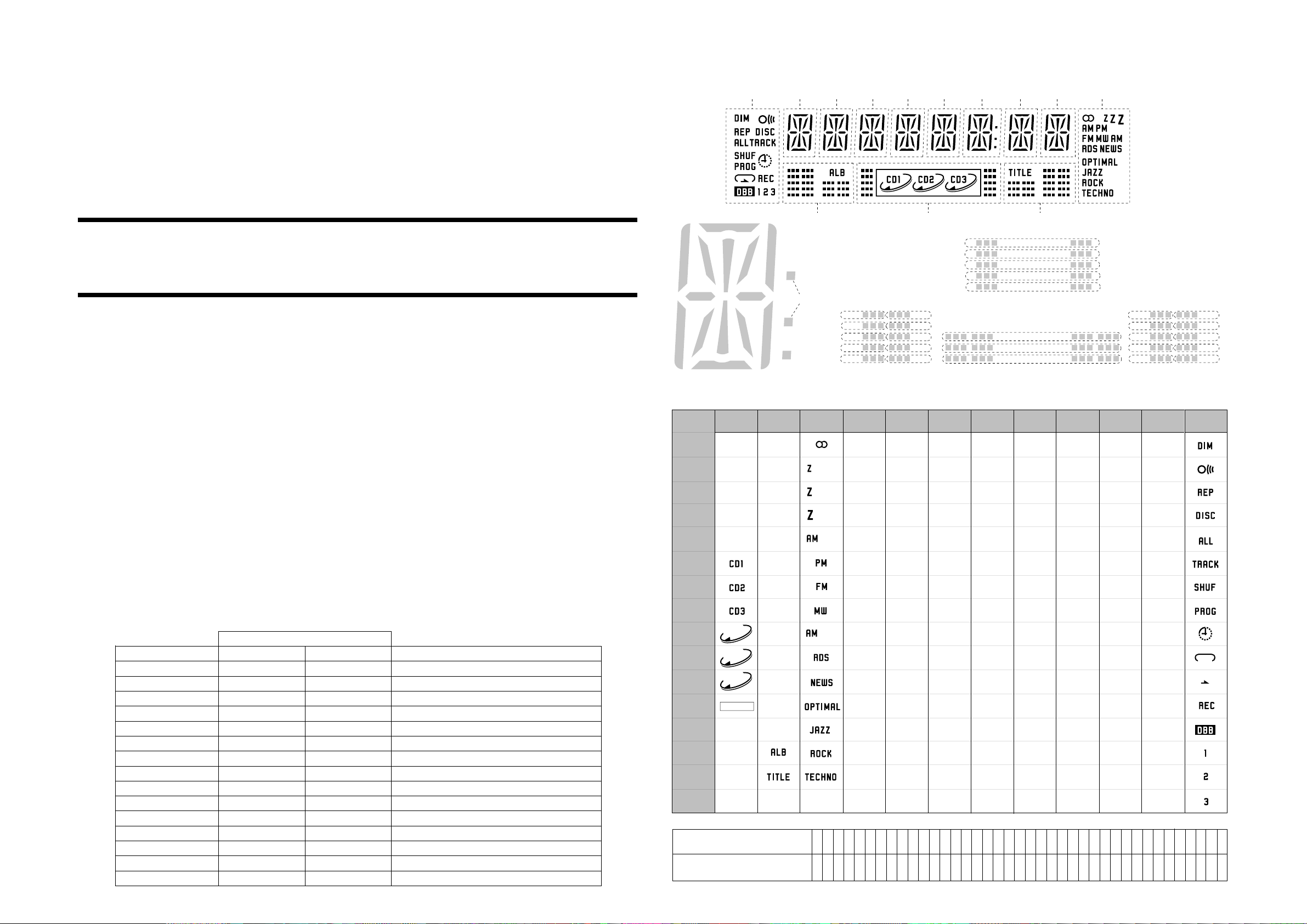
FTD DISPLAY PIN CONNECTIONS
FRONT BOARD
e
f
h
g
r
(2G - 9G)
1G
a
j
k
m
n
p
d
2G
b
Col 1
c
Dp
3G
11G
B5
B4
B3
B2
B1
4G
5G
6G
12G 11G
B10
B9
B8
B7
B6
7G
8G
B5
B4
B3
B2
B1
(12G)
B13
B12
B11
(11G)
9G
10G
B10
B9
B8
B7
B6
B5
B4
B3
B2
B1
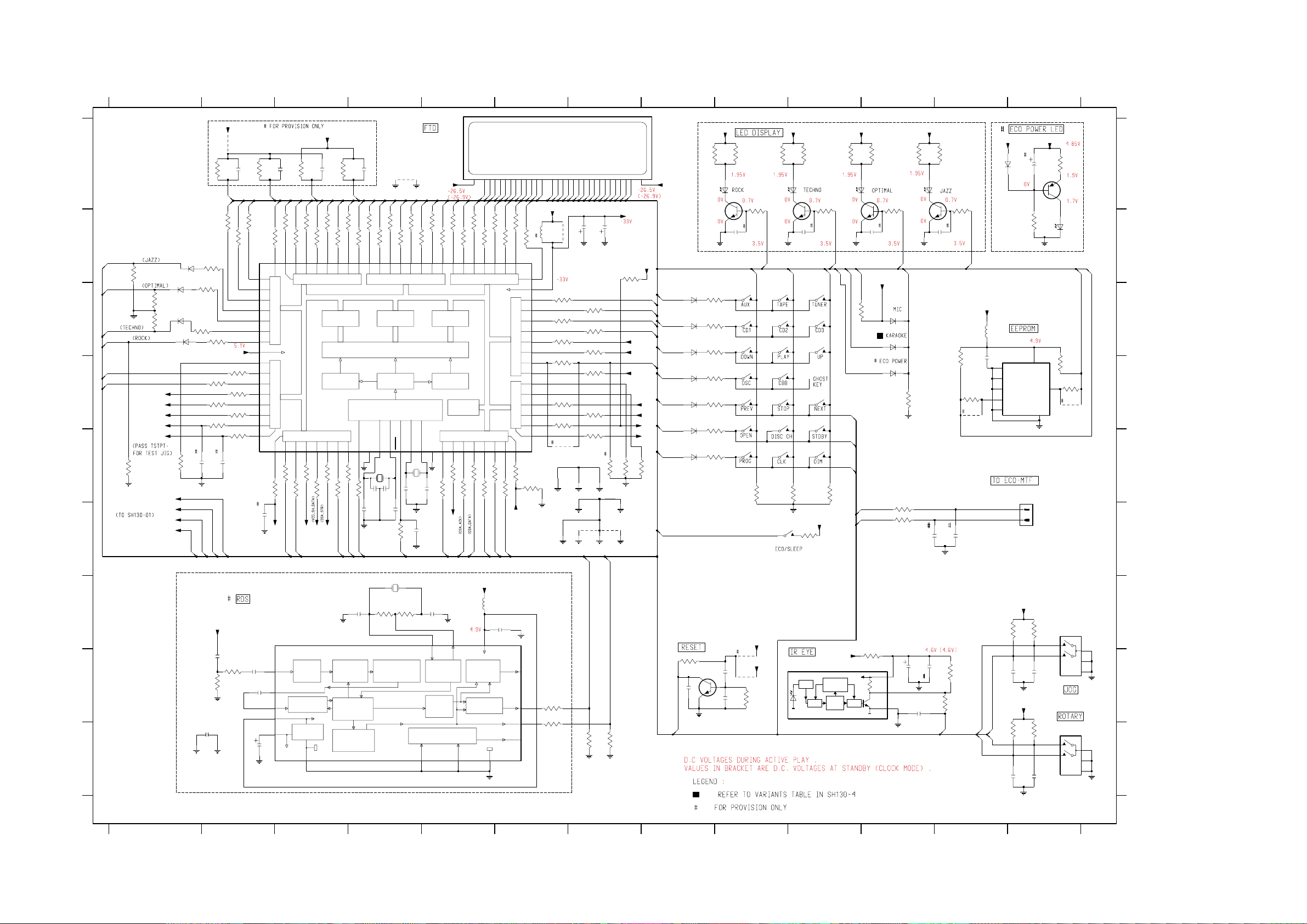
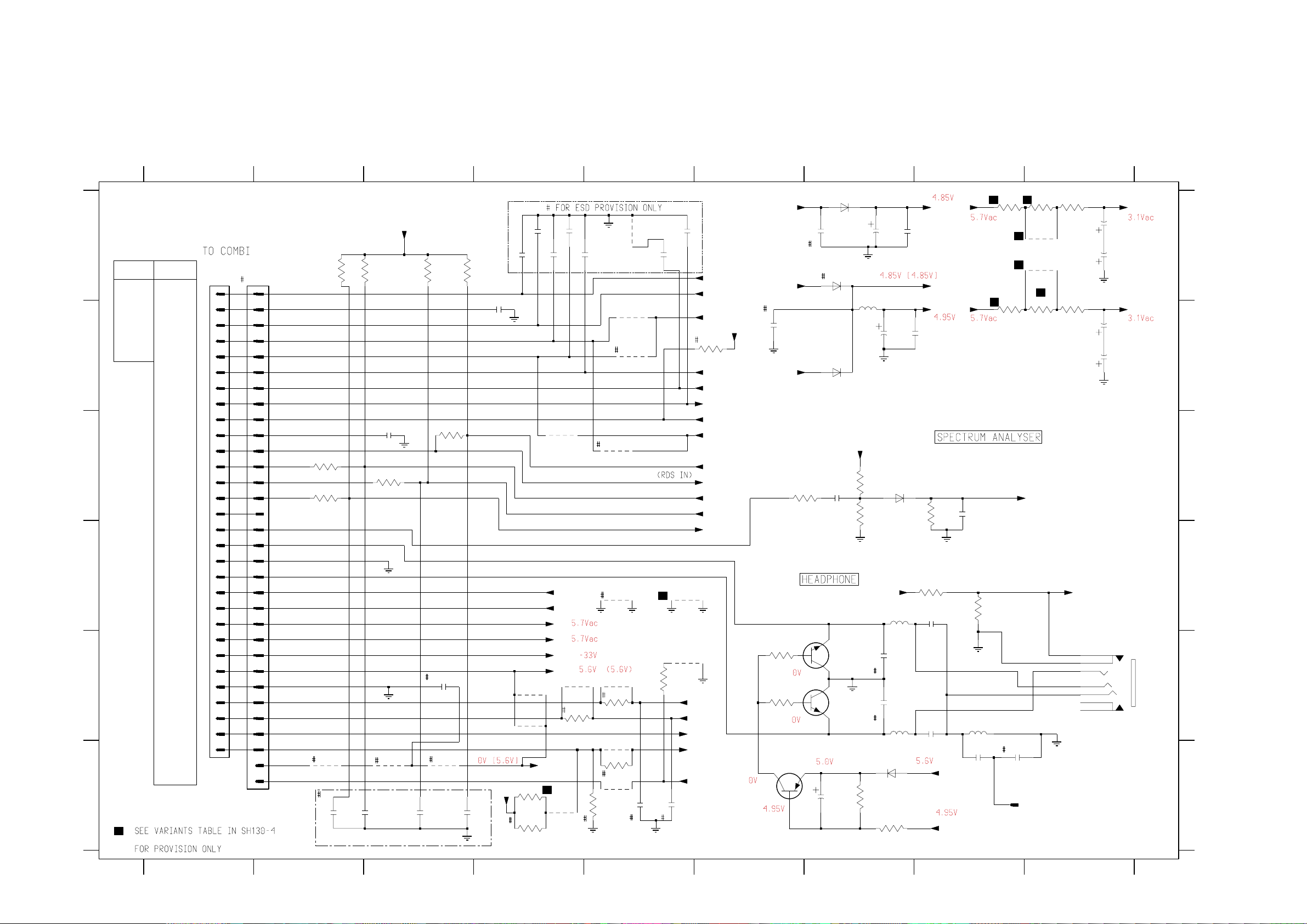
TABLE OF CONTENTS
Variation Table and FTD Display pin connection ............ 6-1
Chip Layout...................................................................... 6-2
Component Layout .......................................................... 6-3
Circuit Diagram - Karaoke part........................................ 6-4
Circuit Diagram - Microprocessor part ............................ 6-5
Circuit Diagram - Headphone / Miscellaneous part ........ 6-6
Electrical Parts List .......................................................... 6-7
Stroke Versions
Features / Item no. /21/21M/33 /30/37 Remarks
Simple Karaoke x Mic Detect x RDS - ECO Power LED - 1800 x - Mic Socket
1802 x - Karaoke
3492 820R 820R NTC
3565 4R7 2R2 FTD Filament
3566 - 2R2 FTD Filament
3567 4R7 2R2 FTD Filament
3568 - 2R2 FTD Filament
4411 x - Karaoke
6429 x - Karaoke
9401 x - FTD Filament
9402 x - FTD Filament
12G
P1
P2
P3
P4
P5
B1
B2
B3
B4
B5
P6
P7
P8
P9
P10
P11
(1)
(2)
(3)
P12
P13
P14
P15
P16
FTD DISPLAY PIN NO.
FUNCTION
-
-
-
-
11G
B1
B2
B3
B4
B5
B6
B7
B8
B9
B10
B11
B12
B13
-
10G
(Left)
(Middle)
(Right)
(Up)
(Low)
-
3
3
8
9
-
F
2
12
2G
1G7G
a
h
j , p
k
b
f
m
g
c
e
r
n
d
-
-
-
1
9
8
7
6
P
P
P
P
13
14
15
16
2
5
4
3
F
-
P
-
1
9G
a
h
j , p
k
b
f
m
g
c
e
r
n
d
-
-
-
3
3
3
5
6
7
1
-
G
8G
a
h
j , p
k
b
f
m
g
c
e
r
n
d
-
-
-
3
3
3
3
3
3
0
2
4
1
3
6
4
2
5
G
G
G
G
G
a
h
j , p
k
b
f
m
g
c
e
r
n
d
Col
Dp
-
2
2
2
9
8
7
7
8
9
10
G
G
G
G
6G
a
h
j , p
k
b
f
m
g
c
e
r
n
d
-
-
-
2
6
11
2
2
2
2
2
5
4
3
12
-
G
G
5G
a
h
j , p
k
b
f
m
g
c
e
r
n
d
-
-
-
2
2
1
1
0
9
-
-
P
P
1
2
4G
a
h
j , p
k
b
f
m
g
c
e
r
n
d
-
-
-
1
1
1
1
1
8
6
4
7
5
P
P
P
P
P
3
5
7
4
6
3G
a
h
j , p
k
b
f
m
g
c
e
r
n
d
-
-
-
1
1
1
1
3
2
1
0
P
P
P
P
8
9
10
11
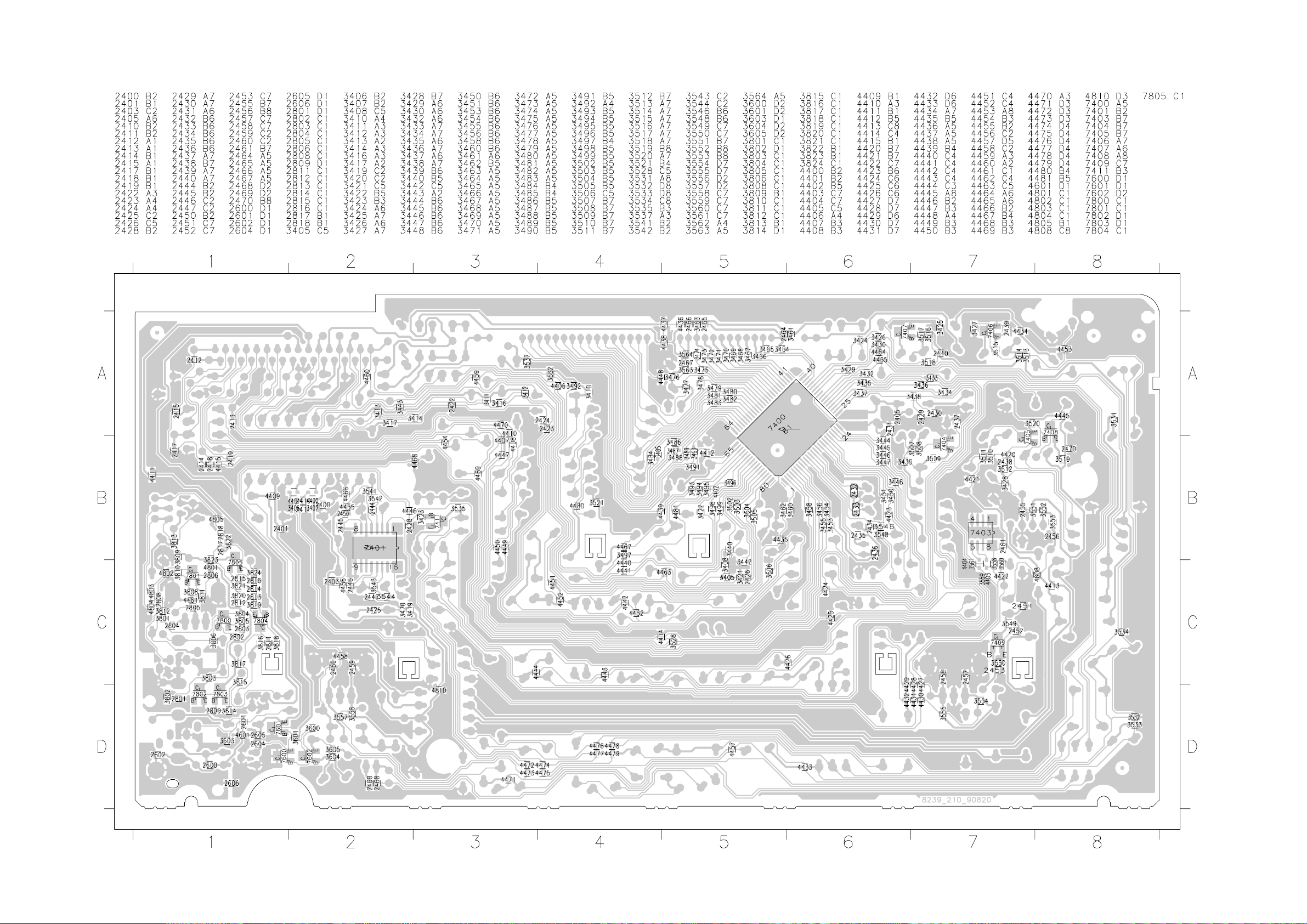
CHIP LAYOUT
This assembly drawing shows a summary of all possible versions. For components used in a specific version see schematic diagram and respective parts list.
6-26-2
3139 118 3461 pt 1 dd wk149
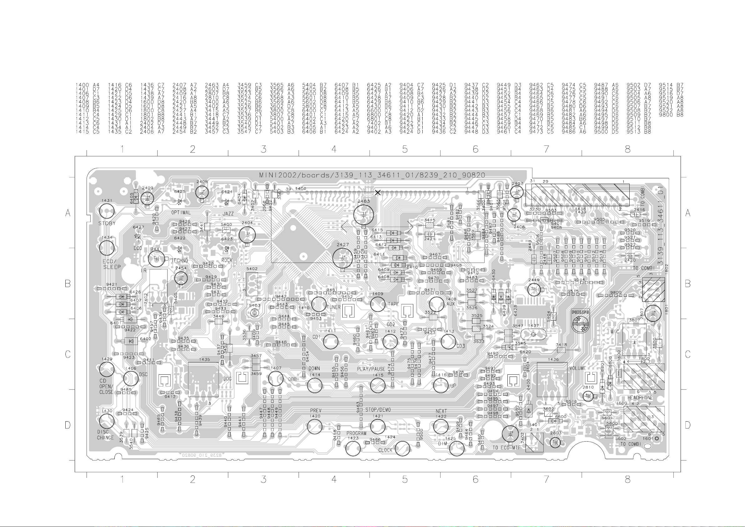
COMPONENT LAYOUT
This assembly drawing shows a summary of all possible versions. For components used in a specific version see schematic diagram and respective parts list.
6-3 6-3
3139 118 3461 pt 1 dd wk149
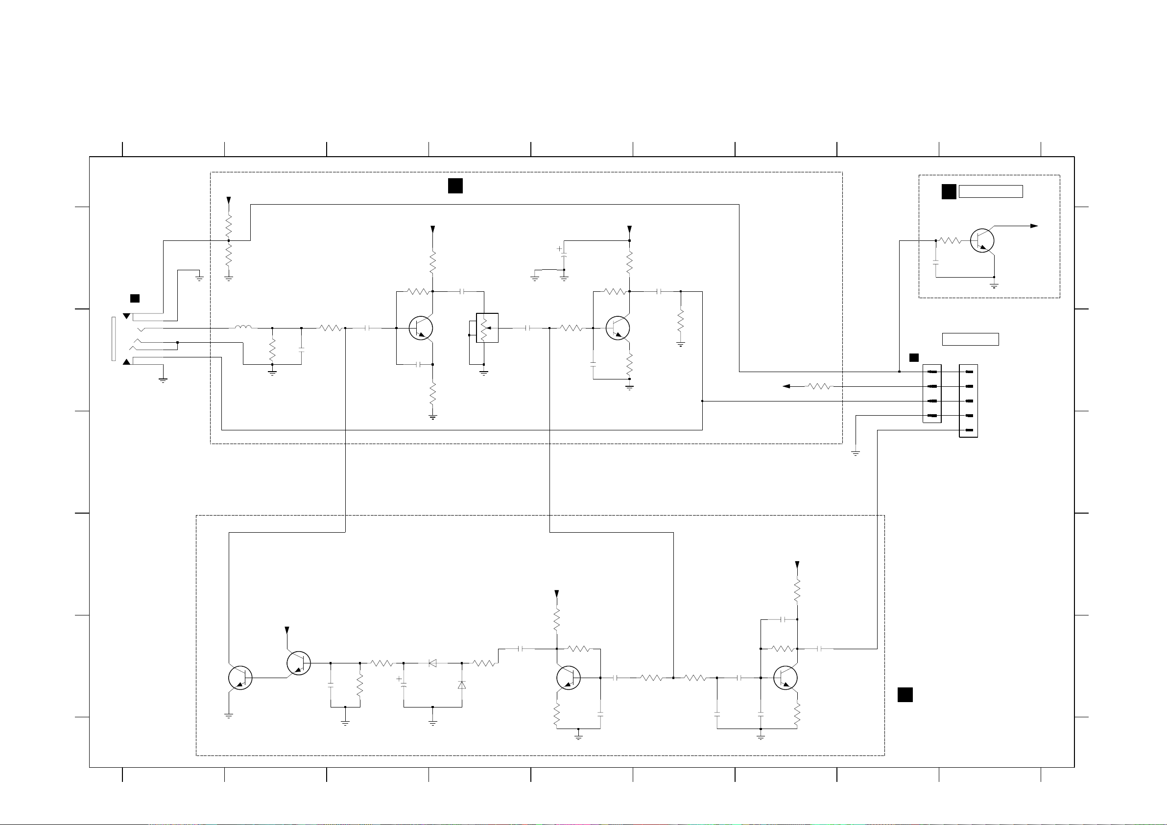
CIRCUIT DIAGRAM - KARAOKE PART
6-4 6-4
A
B
1800 A1
1801 B9
1802 B8
2428 A9
2801 B2
2802 B3
1800
TC38
2803 B3
2804 A4
2805 B4
2806 B5
2807 A5
2808 A6
2809 E2
2810 E3
2811 E4
2812 E5
2813 E5
2814 E6
2815 E7
2816 E7
2817 D7
2818 E7
3423 A9
3800 A1
3801 A1
3802 B2
3803 B3
3804 A3
3805 A3
3806 B3
3807 B4
3808 B5
3809 A5
3810 A5
3811 B5
3812 B6
3813 B7
3814 E3
3815 E3
3816 E4
3817 E5
3818 E5
3819 E5
3820 E6
3821 E6
3822 E7
3823 D7
3824 E7
5800 B2
6800 E4
6801 E4
7411 A9
7800 B4
7801 B5
7802 E2
7803 E2
7804 E5
7805 E7
123456789
SIMPLE KARAOKE
47u
2807
2804
470n
2805
470n
3807
RK09D
20K
GND_A
MIC
GND_A
3808
470R
1.4V
2806
3810
1M
680p
+12V_A
3809
8.9V
7801
BC847B
0V
3811
GND_A
560R
330R
2808
1u
3812
GND_A
10K
+12V_A
3813
470R
11.9V
MIC DETECT
7411
BC847B
D
MicDet
(TO SH 130-1)
1u
3423
10K
2428
0V
0.7V
TO COMBI
#
1
2
3
4
5
1801
MIC_DET
+12V_A
MIC_SK
GND A
MIC_VCD
1802
1
2
3
4
MIC
+12V_A
0.7V
3805
1M
2803
1n
+12V_A
3804
7800
BC847B
3806
MIC
2K7
5.8V
0V
33R
4K7
6K8
3801 3800
MIC
GND_A
4
2
7
1
6
3
5
5800
22u
3802
MIC
10K
2801
3803
10K
4n7
2802
100n
A
B
C
D
E
7802
BC847B
GND_A
+12V_A
7803
BC847B
2809
GND_A
100n
# VCD
3815
150K
1M
3814
2810
6800
1N4148
10u
GND_A
6801
3816
1K
1N4148
2811
100n
+12V_A
7804
BC847B
3817
3819
1K8
3818
1M
100R
GND_A
2813
2812
1u
1n
3820
10K
3821
10K
2814
2815
1u
100n
2816
GND_A
2817
680p
3822
1M
680p
+12V_A
3823
7805
BC847B
3824
12K220R
2818
100n
GND_A
FE-ST-VK-N
FE-ST-VK-N
SEE V ARIANTS TABLE IN SH130-4
FOR PROVISION ONLY
#
C
D
E
123456789
6-5
CIRCUIT DIAGRAM - MICROPROCESSOR PART
6-5
3474 B3
3475 B4
3476 B4
3477 B4
3478 B4
3479 B4
3480 B4
3481 B4
3482 B5
3483 B5
3484 B5
3485 B5
3486 B5
3487 B5
3488 B5
3489 B6
3490 B6
3491 B6
3493 C6
3494 C7
3495 C6
3496 C7
3497 C6
3498 D6
3499 D7
3502 D6
3503 D7
3504 D6
3505 E7
3506 E7
3507 A8
3508 A9
3509 A9
3510 A9
3511 A10
3512 A10
3513 A10
3514 A11
3515 A11
3516 A11
3517 A12
3518 A12
3519 A13
3520 B13
3521 C9
3522 C9
3523 C9
3524 D9
3525 D9
3526 D9
3527 E9
3531 F10
3532 E9
3533 E10
3534 E10
3535 C10
3536 F4
3537 D11
3539 F11
3540 F11
3541 H2
3542 H2
3543 G4
3544 G4
3545 H6
3546 I7
3547 H6
3548 I7
3549 H8
3550 H9
3551 H11
3552 H12
3553 H12
3554 G13
3555 G13
3556 I13
3557 I13
3558 D12
3559 D12
3560 D13
3561 D13
3563 A3
3564 A3
4402 E6
4403 D12
4404 D13
4412 F7
4436 A2
5401 B6
5402 E4
5403 E4
5404 G5
5405 C12
6404 B1
6405 C1
6406 C1
6407 C1
6408 C8
6409 C8
6410 C8
6411 D8
6412 D8
6413 D8
6415 E8
6422 A9
6423 A9
6424 A11
6425 A10
6426 A12
6427 B13
6428 C11
6429 C11
6430 D11
7402 H10
7403 C12
7404 B9
7405 B10
7406 B10
7407 B11
7408 A13
7409 H9
9406 B6
9408 A4
9409 F7
9411 H9
9412 H9
1 2345678910111213
-FTD
-FTD
4436
A
B
Led4
10K
3425
Led3
3427
Led2
Led1
TpShData
TpShStr
3439
10K
D
3428
Cd_On
HP_Mute
TuCe
TuClk
C
D
E
D
Mute
10K
10K
I2_DAT
I2_CLK
CdSiLd
CdSiCl
6405
1N4148
6406
1N4148
6407
1N4148
3441
6404
1N4148
10K
F
CdSiCl
3429
1K
2429
3426
1K
CdSiLd
3424
D
3461
1K
3430
3433
1K
3435
1K
3437
1K
470p
I2_CLK
10K
G01
G01
3464
1K
3432
3434
3436
3438
2430
470p
100p
2464
G03
G02
1K
3466
1K
3465
+H
1K
1K
1K
1K
TMP87CN71
7400
3463
1K
40 P66
39 P65
38 P64
37 P63
36 P62
35 P61
34 P60
33 VDD
32 P07
31 P06
30 P05
29 P04
28 P03
27 P02
26 P01
25 P00
10K
G10
G04
3467
41
P6742P7043P71
3444
470p
2431
D
I2_DAT
2465
I/O PORT 0 I/O PORT 6
TuD at
G05
3468
1K
VDD
3445
1K
10K
3564
100p
G11
G08
G07
G06
1K
1K
3470
1K
3469
3471
44
45
P72
P7346P7447P7548P7649P7750P8051P8152P8253P8354P8455P8556P8657P8758P9059P9160P9261P9362P9463P9564P96
I/O PORT 7 I/O PORT 9
100p
2466
G09
3472
1K
DATA MEMORY
1024X8 BIT
G10
1K
3473
(RAM)
3563
G11
3474
1K
10K
G12
G12
1K
3475
2467
P01
3476
1K
100p
P02
P03
1K
3478
1K
3477
I/O PORT 8
PROGR MEMORY
(ROM)
48KX8 BIT
FTD
P04
1K
3479
9408
P05
3480
1K
E
P06
1K
3481
P07
3482
1K
P08
1K
3483
PROGRAM
COUNTER
C P U
1K
3446
I2_CLK
3447
1K
I2_DAT
I/O PORT 3
1K
3448
CdShClk
CdShData
16 BIT
TIMER/COUNTER
P30
P3119P3220P3321P3422P3523P3624P37
17
18
1K
3451
3449
1K
1K
3450
CdPore
RdsDat
RdsClk
INTERRUPT
CONTROLLER
CLOCK/TIMING CONTROLLER
(I/O PORT 2)
VSS
P20
XOUT
XIN
15
13
14
16
CST
D
5402
1K
8MHz
3452
10K
2432
33p
33p
2433
RES
VOLA
RESET
12
3536
Reset
5403
DT-38
32K768
15p
2435
1K
P2111P22
10
XTAL
2434
D
2436
10n
TEST
9
15p
TIMER/COUNTER
D
VOLB
1437
AT-51
47p
4M332
3543
220K
RECONSTRUCTION
FILTER
G
TuEnable
1n
2443
3542
1K5
10K
H
3541
D
2448
47n
TU
I
D
2444
560p
2445
560p
2449
2u2
D
7401
SAA6579T
4
MUX
8
SCOUT
CIN
7
5
VDDA
3
VREF
ANTI-
ALIASING
FILTER
CLOCKED
COMPARATOR
VP1
REFERENCE
VOLTAGE
VSSA
6
2446
D
57 Khz
BANDPASS
(8th ORDER)
COSTAS LOOP
VARIABLE AND
FIXED DIVIDER
CLOCK
REGENERATION
AND SYNC
2447
3544
2K2
47p
13
OSCI
OSCILLATOR
AND
DIVIDER
BIPHASE
SYMBOL
DECODER
TEST LOGIC AND OUTPUT
SELECTOR SWITCH
MODE
9
F2x
P09
3484
1K
8 BIT
6 BIT A/D-
CONVERTER
3454
10K
3453
LPC
D
14
OSCO
TEST
1400
12-ST-29GNK
343539 56789
G12
G11
G10
G09
G08
G07
G06
G05
G04
G03
G02
G01
P10
P11
P12
P13
P14
P15
P16
1K
1K
1K
1K
3485
I/O PORT 1
1K
3455
CdSiLd
3486
1K
3456
1K
CdSiCl
3487
1K
3457
JOGB
+F
5404
3488
1K
3458
10K
2u2
3490
5401
1K
1K
3489
3491
P97 65
1K
3459
JOGA
66VKK
67P40
68P41
69P42
70P43
71P44
I/O PORT 4I/O PORT 5
72P45
73P46
74P47
75P50
76P51
77P52
78P53
79P54
P55 80
P10
P113P124P135P146P157P168P17
1
2
1K
3460
1M
10K
3462
PWDN
VKK
RC5
2450
100n
QUALITY
BIT
GENERATOR
DIFFERENTIAL
DECODER
10
12
VDDD
VSSD
11
QUAL
RDDA
RDCL
T57
D
1
2
16
15
D
-VKK
2u2
D
3547
10K
3545
10K
+5V6 +5V6
3508
470R
3507
470R
P15
P16
3443
1K
OPTIONS
TuStereo
HPDet
LPSWakeUp
CdSwinfo
Amp_On
CdShStr
10K
3442
D
110111213
KEY0
KEY1
KEY2
NTC
F1x
6423
7404
BC847B
2437
22p
D
+F
3521
330R
3522
330R
3523
330R
3524
330R
3525
330R
3526
330R
3527
330R
1408
1411
1414
1406
1420
1429
1423
6408
P09
1N4148
6409
P08
1N4148
6410
P07
1N4148
6411
P06
1N4148
6412
P05
SA
1N4148
6413
P04
1N4148
6415
P03
10K
1N4148
LPSWakeUp
1415161718192024252627282930313233
P12
P13
P01
P02
P03
P04
P05
P06
P07
2427
9406
P14
P08
P09
P10
P11
-FTD
22u
22u
2463
FTD
D
3493
1K
3494
1K
3497
1K
3498
1K
1K
3496
1K
3422
1K
3499
3495
1K
3502
3503
1K
3504
100R
4402
RES
1K
3505
1K
10K
3506
3440
XTAL
D
I2C
4412
E
G
9409
D
TU
CD
10K
KEY0
3532
Led1
470K
3510
3511
470R
6422
7405
BC847B
2438
D
KEY1
1409
1412
1415
1407
1421 1422
1430
1424
3533
470K
D
1434
3531
10K
470R
3512
10K
1410
1413
1416
1431
1425
+LPS
KEY2
3534
Led2
P05x
470K
3513
7406
BC847B
P04x
P05x
P04x
P03x
+5V6
470R
6425
3535
3514
2439
22p22p
D
P03x
4K7
TpShData
TpShStr
470R
MicDet
35153509
10K
6428
1N4148
6429
1N4148
6430
1N4148
3539
1K
3540
1K
Led3
3537
3516
7407
BC847B
OPTIONS
470K
E
+5V6
6424
470R
D
2468
3517
2440
22p
100p
470R
2469
3518
10K
3558
3559
4403
100p
6K8
+5V6
6426
1N4148
2441
3520
47K
+LPS
47u
3519
6427
820R
7408
BC857B
D
Led4
I2_CLK
+F
2u2
5405
7403
M24C01
2461
100n
1
2
3
6
1K
7
TpShData
TpShStr
E0
E1
E2
SCL
WC_
8
VCC
SDA
VSS
4
I2C
1401
1
Tp_Rec
2
Tp_Play
I2_DAT
6K8
3560
3561
5
1K
4404
EH-S
D
RdsClk
RdsDat
+F
1435
EC12
10K
3555
24
1 3
5
MT2
2458
10n
MT1
G
G
1436
EC12
10K
3557
2
1 3
5
MT2
4
MT1
2460
10n
G
3548
10K
JOGB
VOLA
JOGA
VOLB
3554
2457
3556
2459
10n
+F
10K
10n
+LPS
2452
2453
10n
100n
9411
9412
3550
+F
100K
7402
TSOP2236
INP
PIN
AGC
CTRL
CIRCUIT
BAND
PASS
3549
10K
2451
7409
BC847B
100n
D
Reset
10K
10K
3546
D
D
+LPS
DEM
3551
100R
OUT
4u7
2456
2n2
D
2455
47n
10K
3552
1K
3553
RC5
2454
2VS
1
3GND
D
G
1400 A5
1401 E13
1406 D9
1407 D9
1408 C9
1409 C9
1410 C10
1411 C9
1412 C9
1413 C10
1414 C9
1415 C9
A
1416 C10
1420 D9
1421 D9
1422 D10
1423 E9
1424 E9
1425 E10
1429 D9
1430 D9
1431 D10
1434 F10
1435 G13
1436 I13
B
1437 G4
2427 B7
2429 E1
2430 E2
2431 F2
2432 F4
2433 F4
2434 F4
2435 E4
2436 E5
2437 B9
C
2438 B10
2439 B11
2440 B12
2441 A13
2443 H2
2444 H2
2445 H2
2446 G4
2447 G5
2448 I2
2449 I2
2450 G6
D
2451 H8
2452 H9
2453 H9
2454 H11
2455 H11
2456 H11
2457 H13
2458 H13
2459 I13
2460 I13
2461 D12
2463 B7
E
2464 A2
2465 A3
2466 A3
2467 A4
2468 F11
2469 F12
3422 C7
3424 B2
3425 B1
3426 C2
3427 C1
F
3428 C1
3429 C2
3430 C2
3432 D2
3433 D2
3434 D2
3435 D2
3436 D2
3437 D2
3438 E2
3439 E1
3440 E7
G
3441 E1
3442 E7
3443 B7
3444 E2
3445 E3
3446 E3
3447 E3
3448 E3
3449 E3
3450 E3
3451 E3
3452 E4
H
3453 F5
3454 E5
3455 E5
3456 E5
3457 E5
3458 E5
3459 E6
3460 E6
3461 A2
3462 E6
3463 A2
I
3464 B2
3465 B2
3466 B2
3467 B2
3468 B3
3469 B3
3470 B3
3471 B3
3472 B3
3473 B3
1 2345678910111213
6-6
CIRCUIT DIAGRAM - HEADPHONE / MISCELLANEOUS PART
6-6
A
B
C
D
E
F
1438 A1
1439 A1
1600 E9
1601 F8
VCD NON-VCD
DSA_STR
DSA_ACK
DSA_DATA
SH_DATA
#
2400 E3
2401 A7
2402 A7
2403 A7
CD_SHDATA
CD_SHCLK
CD_SHSTR
CD_SWINFO
TU_ENABLE
TU_STEREO
+5V6_ECO
2404 B7
2405 B7
2406 A9
2407 A9
2408 B9
2409 B9
2410 F5
2411 F5
2412 B4
2413 C3
2414 A4
2415 A4
2416 A4
2417 A4
2418 A4
2419 A5
2420 A5
2421 F2
2422 F2
2423 F3
2424 F3
2425 C7
2426 C8
2470 B6
2600 D8
2601 E8
2602 F8
2603 F7
2604 E7
2605 E7
2606 F8
3400 A9
3402 B9
3405 F5
3406 E5
3407 E4
3408 F5
3410 A2
3411 A2
3412 A3
3413 A3
3414 C2
3415 C2
3416 C3
3417 C3
3418 C7
3419 C7
3420 C7
3421 C8
3492 F4
3528 E5
3562 F4
3565 A8
3566 A9
3567 B8
3568 B9
3569 B6
3600 E6
3601 E6
3602 D8
3603 D8
3604 F7
3605 F7
4400 E4
4401 E5
4405 F5
4406 F4
4407 B5
4408 C4
4409 E4
4410 B5
4411 D5
4413 E4
4414 E5
4415 A5
4460 F2
5400 B7
5600 D7
5601 E7
5602 E8
6400 A7
6401 A7
6402 B7
6420 C7
6600 F7
7600 E7
7601 E7
7602 F6
123456789
CD_PORE
CD_GND
CD_SILD
CD_SICL
CD_ON
TU_GND
TU_DATA
TU_CLK
D_GND
SA_IN
HP_RIGHT
HP_GND
HP_LEFT
AMP_ON
MUTE
F2
F1
-Vkk
+5V6
D_GND
I2C_CLK
I2C_DATA
PWDN
NTC
LPC
1
2
3
4
5
6
7
8
9
10
11
12
13
14
15
16
17
18
19
20
21
22
23
24
25
26
27
28
29
30
1439
FE-ST-VK-N
2401
2603
6400
1N4003
100n
6401
1N4003
6402
1N4003
2425
47n
7600
BC817-25
7601
BC817-25
1u
5400
2u2
+F
3419
3420
HP
3604
2402
D
2404
82K
82K
D
4K7
100u
100u
D
6420
1N4148
+5V6
5600
2u2
100p
2604
100p
2605
5601
2u2
6600
1N4148
3605
10K
+5V6
+F
2414
TU
2423
3412
10K
3417
2400
100n
95144460 9506
47p
10K
10K
3411
3414
1K
3415
1K
2421
3410
47p
2422
2413
100p
3416
1K
HP
D
47p
1438
1
2
3
4
5
6
7
8
9
10
11
12
13
14
15
16
17
18
19
20
21
22
23
24
25
26
27
28
29
30
31
32
1K
3413
2424
10K
2412
100n
+F
47p
TU
CD
4409
4413
3492
2K2
3562
2K2
2415
47p
+5V6_ECO
47p
2416
4408
Amp_On
Mute
F2
F1
-VKK
+5V6
4406
2417
47p
4400
3407
1K
47p
2418
47p
3408
CD
150K
D
9410
9404
D
4401
3406
1K
4405
3405
1K
9487
4415
(DSA_ACK)
4407
4410
(DSA_DATA)
I2C
2410
2419
SA_IN
HP_RIGHT
HP_LEFT
GND_A
3528
10p
2411
I2C
47p
4411
4414
10K
2420
I2_CLK
I2_DAT
10p
47p
3569
10K
PWDN
NTC
LPC
CdPore
CdSiLd
CdShData
+F
CdShClk
CdShStr
CdSwinfo
Cd_On
CdSiCl
TuCe
TuEnable
TuDat
TuClk
TuStereo
HP
TU
+5V6_ECO
100n
2470
D
+5V6
3600
1K
3601
1K
7602
BC857B
3418
1K5
2403
2405
100n
100n
3421
3602
1K
2600
22n
2601
22n
+F
+LPS
+H
470K
+5V6
HP_Mute
F1
F2
2426
D
220n
4K7
3603
HP
5602
2u2
2602
100n
(FROM SH 130-1)
3565
2R2
3567
2R2
(TO SH 130-1)
2606
22n
1601
RT-01T
1
3400
3566
4R7
2R2
9401
9402
3402
3568
4R7
2R2
SA
HP
(ESD WIRE TO COMBI PCB)
HPDet
1600
TC38
4
2
7
1
6
3
5
2406
2407
FTD
2408
2409
FTD
(TO SH 130-1)
9401 A9
9402 A9
9404 D5
9410 C5
F1x
4u7
(TO SH 130-1)
4u7
F2x
4u7
(TO SH 130-1)
4u7
9487 F5
9506 F3
9514 F3
A
B
C
D
E
F
123456789

MISCELLANEOUS
1400 3139 110 52850 FTD Display 12-ST-29GNK
1406 2422 128 02917 Tact Switch
1407 2422 128 02917 Tact Switch
1408 2422 128 02917 Tact Switch
1409 2422 128 02917 Tact Switch
1410 2422 128 02917 Tact Switch
1411 2422 128 02917 Tact Switch
1412 2422 128 02917 Tact Switch
1413 2422 128 02917 Tact Switch
1414 2422 128 02917 Tact Switch
1415 2422 128 02917 Tact Switch
1416 2422 128 02917 Tact Switch
1420 2422 128 02917 Tact Switch
1421 2422 128 02917 Tact Switch
1422 2422 128 02917 Tact Switch
1423 2422 128 02917 Tact Switch
1424 2422 128 02917 Tact Switch
1425 2422 128 02917 Tact Switch
1429 2422 128 02917 Tact Switch
1430 2422 128 02917 Tact Switch
1431 2422 128 02917 Tact Switch
1434 2422 128 02917 Tact Switch
1435 2422 129 16707 Rotary Encoder 24P
1436 2422 129 16708 Rotary Encoder 24P
1439 2422 025 17414 Flex Socket 30pin Hort.
1600 2422 026 05059 Headphone Socket
1800 2422 026 05059 Mic Socket /21/21M
1802 4822 265 11 183 Flex Socket 4pin Hort. /21/21M
CAPACITORS
2402 4822 124 23432 100µF 20% 10V
2403 4822 126 14305 100nF 10% 16V
2404 4822 124 23432 100µF 20% 10V
2405 4822 126 14305 100nF 10% 16V
2406 4822 124 12032 4,7µF 20% 50V
2407 4822 124 12032 4,7µF 20% 50V
2408 4822 124 12032 4,7µF 20% 50V
2409 4822 124 12032 4,7µF 20% 50V
2412 4822 126 14305 100nF 10% 16V
2413 4822 122 31765 100pF 2% 63V
2425 3198 017 34730 47nF 16V
2426 4822 126 13879 220nF +80/-20% 16V
2427 3198 028 52290 22µF 20% 50V
2428 3198 017 41050 1µF 10V /21/21M
2432 2222 867 15339 33pF 50V
2433 2222 867 15339 33pF 50V
2434 5322 126 11583 10nF 10% 50V
2435 4822 122 33752 15pF 5% 50V
2436 4822 122 33752 15pF 5% 50V
2451 4822 126 14305 100nF 10% 16V
2452 4822 126 14305 100nF 10% 16V
2453 5322 126 11583 10nF 10% 50V
6-7
2454 4822 124 12032 4,7µF 20% 50V
2456 4822 126 14238 2,2nF 50V
2457 5322 126 11583 10nF 10% 50V
2458 5322 126 11583 10nF 10% 50V
2459 5322 126 11583 10nF 10% 50V
2460 5322 126 11583 10nF 10% 50V
2461 4822 126 14305 100nF 10% 16V
2463 3198 028 52290 22µF 20% 50V
2600 4822 126 14494 22nF 10% 25V
2601 4822 126 14494 22nF 10% 25V
2602 4822 126 14305 100nF 10% 16V
2603 4822 124 22651 1µF 20% 50V
2801 4822 126 13193 4,7nF 10% 63V /21/21M
2802 4822 126 14305 100nF 10% 16V /21/21M
2803 5322 126 11578 1nF 10% 50V /21/21M
2804 3198 017 44740 470nF 10V /21/21M
2805 3198 017 44740 470nF 10V /21/21M
2806 4822 126 13909 680pF 10% 50V /21/21M
2807 4822 124 81286 47µF 20% 16V /21/21M
2808 3198 017 41050 1µF 10V /21/21M
RESISTORS
3400 4822 050 24708 4R7 1% 0,6W
3402 4822 050 24708 4R7 1% 0,6W
3410 4822 051 30103 10k 5% 0,062W
3411 4822 051 30103 10k 5% 0,062W
3412 4822 051 30103 10k 5% 0,062W
3413 4822 051 30103 10k 5% 0,062W
3414 4822 051 30102 1k 5% 0,062W
3415 4822 050 11002 1k 1% 0,4W
3416 4822 051 30102 1k 5% 0,062W
3417 4822 051 30102 1k 5% 0,062W
3418 4822 116 52243 1k5 5% 0,5W
3419 4822 117 12864 82k 5% 0,6W
3420 4822 117 12864 82k 5% 0,6W
3421 4822 051 30474 470k 5% 0,062W
3422 4822 051 30102 1k 5% 0,062W
3423 4822 051 30103 10k 5% 0,062W /21/21M
3424 4822 051 30102 1k 5% 0,062W
3425 4822 051 30103 10k 5% 0,062W
3426 4822 051 30102 1k 5% 0,062W
3427 4822 051 30103 10k 5% 0,062W
3428 4822 051 30103 10k 5% 0,062W
3429 4822 051 30102 1k 5% 0,062W
3430 4822 051 30102 1k 5% 0,062W
3432 4822 051 30102 1k 5% 0,062W
3433 4822 051 30102 1k 5% 0,062W
3434 4822 051 30102 1k 5% 0,062W
3435 4822 051 30102 1k 5% 0,062W
3436 4822 051 30102 1k 5% 0,062W
3437 4822 051 30102 1k 5% 0,062W
3438 4822 051 30102 1k 5% 0,062W
ELECTRICAL PARTS LIST - FRONT BOARDELECTRICAL PARTS LIST - FRONT BOARD
3439 4822 051 30103 10k 5% 0,062W
3440 4822 051 30103 10k 5% 0,062W
3441 4822 050 21003 10k 1% 0,6W
3442 4822 051 30103 10k 5% 0,062W
3443 4822 051 30102 1k 5% 0,062W
3444 4822 051 30102 1k 5% 0,062W
3445 4822 051 30102 1k 5% 0,062W
3446 4822 051 30102 1k 5% 0,062W
3447 4822 051 30102 1k 5% 0,062W
3448 4822 051 30102 1k 5% 0,062W
3449 4822 050 11002 1k 1% 0,4W
3450 4822 051 30102 1k 5% 0,062W
3451 4822 051 30102 1k 5% 0,062W
3452 4822 050 21003 10k 1% 0,6W
3453 4822 051 30103 10k 5% 0,062W
3454 4822 051 30102 1k 5% 0,062W
3455 4822 051 30102 1k 5% 0,062W
3456 4822 051 30102 1k 5% 0,062W
3457 4822 050 21003 10k 1% 0,6W
3458 4822 051 30102 1k 5% 0,062W
3459 4822 050 21003 10k 1% 0,6W
3460 4822 051 30102 1k 5% 0,062W
3462 4822 051 30105 1M 5% 0,062W
3464 4822 051 30102 1k 5% 0,062W
3465 4822 051 30102 1k 5% 0,062W
3466 4822 051 30102 1k 5% 0,062W
3467 4822 051 30102 1k 5% 0,062W
3468 4822 051 30102 1k 5% 0,062W
3469 4822 051 30102 1k 5% 0,062W
3470 4822 051 30102 1k 5% 0,062W
3471 4822 051 30102 1k 5% 0,062W
3472 4822 051 30102 1k 5% 0,062W
3473 4822 051 30102 1k 5% 0,062W
3474 4822 051 30102 1k 5% 0,062W
3475 4822 051 30102 1k 5% 0,062W
3476 4822 051 30102 1k 5% 0,062W
3477 4822 051 30102 1k 5% 0,062W
3478 4822 051 30102 1k 5% 0,062W
3479 4822 051 30102 1k 5% 0,062W
3480 4822 051 30102 1k 5% 0,062W
3481 4822 051 30102 1k 5% 0,062W
3482 4822 051 30102 1k 5% 0,062W
3483 4822 051 30102 1k 5% 0,062W
3484 4822 051 30102 1k 5% 0,062W
3485 4822 051 30102 1k 5% 0,062W
3486 4822 051 30102 1k 5% 0,062W
3487 4822 051 30102 1k 5% 0,062W
3488 4822 051 30102 1k 5% 0,062W
3489 4822 051 30102 1k 5% 0,062W
3490 4822 051 30102 1k 5% 0,062W
3491 4822 051 30102 1k 5% 0,062W
3492 4822 117 12968 820R 5% 0,62W
6-7
3493 4822 051 30102 1k 5% 0,062W
3494 4822 051 30102 1k 5% 0,062W
3495 4822 051 30102 1k 5% 0,062W
3496 4822 051 30102 1k 5% 0,062W
3497 4822 051 30102 1k 5% 0,062W
3498 4822 051 30102 1k 5% 0,062W
3499 4822 051 30102 1k 5% 0,062W
3502 4822 051 30102 1k 5% 0,062W
3503 4822 051 30102 1k 5% 0,062W
3504 4822 051 30101 100R 5% 0,062W
3505 4822 051 30102 1k 5% 0,062W
3507 4822 051 30471 470R 5% 0,062W
3508 4822 051 30471 470R 5% 0,062W
3509 4822 051 30103 10k 5% 0,062W
3510 4822 051 30471 470R 5% 0,062W
3511 4822 051 30471 470R 5% 0,062W
3512 4822 051 30103 10k 5% 0,062W
3513 4822 051 30471 470R 5% 0,062W
3514 4822 051 30471 470R 5% 0,062W
3515 4822 051 30103 10k 5% 0,062W
3516 4822 051 30471 470R 5% 0,062W
3517 4822 051 30471 470R 5% 0,062W
3518 4822 051 30103 10k 5% 0,062W
3521 4822 051 30331 330R 5% 0,062W
3522 4822 116 52219 330R 5% 0,5W
3523 4822 116 52219 330R 5% 0,5W
3524 4822 116 52219 330R 5% 0,5W
3525 4822 116 52219 330R 5% 0,5W
3526 4822 116 52219 330R 5% 0,5W
3527 4822 116 52219 330R 5% 0,5W
3528 4822 051 30103 10k 5% 0,062W
3531 4822 051 30103 10k 5% 0,062W
3532 4822 051 30474 470k 5% 0,062W
3533 4822 051 30474 470k 5% 0,062W
3534 4822 051 30474 470k 5% 0,062W
3535 4822 051 30472 4k7 5% 0,062W
3536 4822 050 11002 1k 1% 0,4W
3537 4822 051 30474 470k 5% 0,062W
3539 4822 050 11002 1k 1% 0,4W
3540 4822 050 11002 1k 1% 0,4W
3546 4822 051 30103 10k 5% 0,062W
3548 4822 051 30103 10k 5% 0,062W
3549 4822 051 30103 10k 5% 0,062W
3550 4822 117 13632 100k 1% 0,062W
3551 4822 051 30101 100R 5% 0,062W
3552 4822 051 30103 10k 5% 0,062W
3553 4822 051 30102 1k 5% 0,062W
3554 4822 051 30103 10k 5% 0,062W
3555 4822 051 30103 10k 5% 0,062W
3556 4822 051 30103 10k 5% 0,062W
3557 4822 051 30103 10k 5% 0,062W
3558 4822 051 30682 6k8 5% 0,062W

6-8 6-8
ELECTRICAL PARTS LIST - FRONT BOARD
RESISTORS
3559 4822 051 30102 1k 5% 0,062W
3560 4822 051 30682 6k8 5% 0,062W
3561 4822 051 30102 1k 5% 0,062W
3565 4822 050 24708 4R7 5% 0,5W /21/21M
3565 4822 116 81154 2R2 5% 0,5W /30/37
3566 4822 116 81154 2R2 5% 0,5W /30/37
3567 4822 050 24708 4R7 5% 0,5W /21/21M
3567 4822 116 81154 2R2 5% 0,5W /30/37
3568 4822 116 81154 2R2 5% 0,5W /30/37
3600 4822 051 30102 1k 5% 0,062W
3601 4822 051 30102 1k 5% 0,062W
3602 4822 050 11002 1k 1% 0,4W
3603 4822 051 30472 4k7 5% 0,062W
3604 4822 051 30472 4k7 5% 0,062W
3605 4822 051 30103 10k 5% 0,062W
3800 4822 116 52283 4k7 5% 0,5W /21/21M
3801 4822 051 30682 6k8 5% 0,062W /21/21M
3802 4822 051 30103 10k 5% 0,062W /21/21M
3803 4822 051 30103 10k 5% 0,062W /21/21M
3804 4822 051 30272 2k7 5% 0,062W /21/21M
3805 4822 051 30105 1M 5% 0,062W /21/21M
3806 4822 051 30339 33R 5% 0,062W /21/21M
3807 2120 366 90292 Potm Rotary 20K /21/21M
3808 4822 051 30471 470R 5% 0,062W /21/21M
3809 4822 051 30561 560R 5% 0,062W /21/21M
3810 4822 051 30105 1M 5% 0,062W /21/21M
3811 4822 051 30331 330R 5% 0,062W /21/21M
3812 4822 051 30103 10k 5% 0,062W /21/21M
3813 4822 051 30471 470R 5% 0,062W /21/21M
4400 4822 051 30008 0R Jumper 0603
4401 4822 051 30008 0R Jumper 0603
4405 4822 051 30008 0R Jumper 0603
4406 4822 051 30008 0R Jumper 0603
4407 4822 051 30008 0R Jumper 0603
4408 4822 051 30008 0R Jumper 0603
4409 4822 051 30008 0R Jumper 0603
4411 4822 051 30008 0R Jumper 0603 /21/21M
4412 4822 051 30008 0R Jumper 0603
4413 4822 051 30008 0R Jumper 0603
4414 4822 051 30008 0R Jumper 0603
4420 4822 051 30008 0R Jumper 0603
4421 4822 051 30008 0R Jumper 0603
4422 4822 051 30008 0R Jumper 0603
4423 4822 051 30008 0R Jumper 0603
4424 4822 051 30008 0R Jumper 0603
4425 4822 051 30008 0R Jumper 0603
4426 4822 051 30008 0R Jumper 0603
4427 4822 051 30008 0R Jumper 0603
4428 4822 051 30008 0R Jumper 0603
4429 4822 051 30008 0R Jumper 0603
4430 4822 051 30008 0R Jumper 0603
4431 4822 051 30008 0R Jumper 0603
4432 4822 051 30008 0R Jumper 0603
4433 4822 051 30008 0R Jumper 0603
4434 4822 051 30008 0R Jumper 0603
4435 4822 051 30008 0R Jumper 0603
4436 4822 051 30008 0R Jumper 0603 /30/37
4437 4822 051 30008 0R Jumper 0603
4438 4822 051 30008 0R Jumper 0603
4439 4822 051 30008 0R Jumper 0603
4440 4822 051 30008 0R Jumper 0603
4441 4822 051 30008 0R Jumper 0603
4442 4822 051 30008 0R Jumper 0603
4443 4822 051 30008 0R Jumper 0603
4444 4822 051 30008 0R Jumper 0603
4445 4822 051 30008 0R Jumper 0603
4446 4822 051 30008 0R Jumper 0603
4447 4822 051 30008 0R Jumper 0603
4448 4822 051 30008 0R Jumper 0603
4449 4822 051 30008 0R Jumper 0603
4450 4822 051 30008 0R Jumper 0603
4451 4822 051 30008 0R Jumper 0603
4452 4822 051 30008 0R Jumper 0603
4453 4822 051 30008 0R Jumper 0603
4454 4822 051 30008 0R Jumper 0603
4455 4822 051 30008 0R Jumper 0603
4456 4822 051 30008 0R Jumper 0603
4457 4822 051 30008 0R Jumper 0603
4458 4822 051 30008 0R Jumper 0603
4459 4822 051 30008 0R Jumper 0603
4461 4822 051 30008 0R Jumper 0603
4462 4822 051 30008 0R Jumper 0603
4463 4822 051 30008 0R Jumper 0603
4464 4822 051 30008 0R Jumper 0603
4465 4822 051 30008 0R Jumper 0603
4466 4822 051 30008 0R Jumper 0603
4467 4822 051 30008 0R Jumper 0603
4468 4822 051 30008 0R Jumper 0603
4469 4822 051 30008 0R Jumper 0603
4470 4822 051 30008 0R Jumper 0603
4471 4822 051 30008 0R Jumper 0603
4472 4822 051 30008 0R Jumper 0603
4473 4822 051 30008 0R Jumper 0603
4474 4822 051 30008 0R Jumper 0603
4475 4822 051 30008 0R Jumper 0603
4476 4822 051 30008 0R Jumper 0603
4477 4822 051 30008 0R Jumper 0603
4478 4822 051 30008 0R Jumper 0603
4479 4822 051 30008 0R Jumper 0603
4480 4822 051 30008 0R Jumper 0603
4481 4822 051 30008 0R Jumper 0603
4601 4822 051 30008 0R Jumper 0603
4801 4822 051 30008 0R Jumper 0603 /21/21M
4802 4822 051 30008 0R Jumper 0603 /21/21M
ELECTRICAL PARTS LIST - FRONT BOARD
4803 4822 051 30008 0R Jumper 0603 /21/21M
4804 4822 051 30008 0R Jumper 0603 /21/21M
4805 4822 051 30008 0R Jumper 0603 /21/21M
4808 4822 051 30008 0R Jumper 0603
4810 4822 051 30008 0R Jumper 0603
COILS & FILTERS
5400 4822 157 62552 Coil 2,2µH 5%
5402 4822 242 72066 Ceram Resonator 8MHz
5403 2422 543 01069 X’tal Resonator 32,768kHz
5405 4822 157 62552 Coil 2,2µH 5%
5600 4822 157 62552 Coil 2,2µH 5%
5601 4822 157 62552 Coil 2,2µH 5%
5602 4822 157 62552 Coil 2,2µH 5%
5800 4822 157 11235 Coil 22µH 5% /21/21M
DIODES
6400 4822 130 31878 1N4003G
6402 4822 130 31878 1N4003G
6404 4822 130 30621 1N4148
6405 4822 130 30621 1N4148
6406 4822 130 30621 1N4148
6407 4822 130 30621 1N4148
6408 4822 130 30621 1N4148
6409 4822 130 30621 1N4148
6410 4822 130 30621 1N4148
6411 4822 130 30621 1N4148
6412 4822 130 30621 1N4148
6413 4822 130 30621 1N4148
6415 4822 130 30621 1N4148
6420 4822 130 30621 1N4148
6422 9322 178 15676 LTL-8166FTNN
6423 9322 178 15676 LTL-8166FTNN
6424 9322 178 15676 LTL-8166FTNN
6425 9322 178 15676 LTL-8166FTNN
6428 4822 130 30621 1N4148
6429 4822 130 30621 1N4148 /21/21M
6600 4822 130 30621 1N4148
TRANSISTORS & INTEGRATED CIRCUITS
7400 3139 110 52941 TMP87CS71F “C255S52941”
7402 9322 155 22667 IR Receiver TS0P2236ZC1
7403 9965 000 04931 M24C01-WMN6
7404 4822 130 60511 BC847B
7405 4822 130 60511 BC847B
7406 4822 130 60511 BC847B
7407 4822 130 60511 BC847B
7409 4822 130 60511 BC847B
7411 4822 130 60511 BC847B /21/21M
7600 4822 130 42804 BC817-25
7601 4822 130 42804 BC817-25
7602 4822 130 60373 BC857B
7800 4822 130 60511 BC847B /21/21M
7801 4822 130 60511 BC847B /21/21M
Note: Only the parts mentioned in this list are normal
service spare parts.

8-1
MAINS BOARD
8-1
COMPONENT LAYOUT
This assembly drawing shows a summary of all possible versions. For components used in a specific version see schematic diagram and respective parts list.
TABLE OF CONTENTS
Component Layout .......................................................... 8-1
Circuit Diagram ................................................................ 8-2
Electrical parts list............................................................ 8-1
ELECTRICAL PARTS LIST - MAINS BOARD
MISCELLANEOUS
!
1205 9965 000 07788
1210 2422 129 16478
1212 4822 071 55002
Fuse T2A 250V
!
Voltage Selector 5A
!
Fuse T5A 250V
3139 113 3465 pt 1 dd wk149
COILS & FILTERS
5206 4822 157 11832
Note: Only the parts mentioned in this list are normal
service spare parts.
!
Mains Filter 400µH 3A

MAINS CIRCUIT
8-2 8-2
A
A
B
B
C
C
D
D
E
E
1207 C5
1201 A3
1201 A3
1204 C3
1204 C3
1205 C2
1205 C2
1206 C1
1206 C1
1206
1208
1207 C5
1208 D1
1208 D1
1209 C6
1209 C6
1210 E2
1 23456
1
For Low Power Standby version only
5V6_ECO
LPC
6217
6218
1N4148
P
33K
3209
0V
47K
3216
GND_LPC
1
2
1
2
10M
For /37
1211 E6
1211 E6
1212 E5
1212 E5
2201 A9
2201 A9
2202 A4
2202 A4
1N4148
+5.4V
7206
BC547B
0V
1
8201
9202
5206
9204
3217
For /37
2203 A8
2203 A8
2204 A9
2204 A9
2205 A6
2205 A6
2206 A4
2206 A4
6219
BZX79-C5V6
GND_LPC
BC337-25
0V
6215
1N4148
1K
3212
9205
3218
4K7
+12.9V
7203
0V
GND_LPC
For /21 only
1205
T2A
9203
For /21
240V
3
2
1
127V
1210
9206
+C
3220
2211 B9
2211 B9
2212 B10
2212 B10
2213 B3
2213 B3
2214 B8
2214 B8
3221
100R
1N4148
6207
1N4148
6210
1204
Not for /22
9201
LPS
(+12V relay) (+12V relay)
For /22
9
4
6
7
2207 A6
2207 A6
2208 A3
2208 A3
2209 A6
2209 A6
2210 A8
2210 A8
100R
112
5
8
OZ-SS-112L
6
5
4
For /22
2215 B9
2215 B9
3202 A6
3202 A6
3203 A7
3203 A7
3204 A7
3204 A7
9207
1201
T200mA
For /22
2208
220n
2213
For /21,/37
470n
3224
2M2
Mains T ransf ormer
0V
127V
3205 A9
3205 A9
3206 A5
3206 A5
3207 A5
3207 A5
3208 B6
3208 B6
P
2206
3209 B1
3209 B1
3212 B2
3212 B2
3214 B6
3214 B6
3215 B8
3215 B8
3216 B1
3216 B1
3217 D1
3217 D1
3218 A2
3218 A2
3220 A2
3221 A2
3221 A2
3222 A10
3222 A10
3224 B3
3224 B3
5201 A4
5201 A4
5202 A8
5202 A8
5203 A4
5203 A4
5204 B5
5204 B5
5206 C1
5206 C1
4 5 6
1M
3207
BC337-40
EH-B
+C
1N4003
6202
3206
100K
+36.8V
7204
0V
5204
22n
5201
1m
5203
1m
For /22
2202
1N4003
6201
1N4003
6206
47n
6211
1N4003
6214
1N4003
For VCD/MP3 only
1207
1
2
GND_S
1212
T5A
2205
10n
2209
10n
100u
6201 A5
6201 A5
6202 A5
6202 A5
6203 A10
6203 A10
6204 A10
6204 A10
1N4148
+39.6V
+0.3V
BZX79-C39
3214
PW_DN
LPC
5V6_ECO
6205 A6
6205 A6
6206 A5
6206 A5
6207 A3
6207 A3
6208 A8
6208 A8
6205
BC557B
7201
6216
2K2
+39.4V
+39.0V
3203
100u
6213 B10
6213 B10
6214 B5
6214 B5
6215 B2
6215 B2
6216 B6
6216 B6
72 3
7
4M7
6209 A9
6209 A9
6210 A3
6210 A3
6211 A5
6211 A5
6212 B9 9206 E2
6212 B9 9206 E2
10K
3202
2207
3208
470R
For /22 only
1209
EH-B
1
2
3
1
2
3
4
5
6
7
8
9
10
1211
EH-B
3204
330R
7202
BC547B
BC557B
7205
6217 A1
6217 A1
6218 A1
6218 A1
6219 A2
6219 A2
7201 A6
7201 A6
7202 A7
7202 A7
7203 B2
7203 B2
7204 B5
7204 B5
7205 B71210 E2
7205 B7 9202 C1
2203
47n
6208
1N4148
100n
2210
3215
2214
100K
Variation Table
1205x1210x3217
/21
/22
/37
7206 B1
7206 B1
8201 E1
8201 E1
9201 C3
9201 C3
9202 C13220 A2
8910
8 9 10
5202
STBY
4
2
1
3
4n7
2215
5206
x
2n2
x
x
9203 C2
9203 C2
9204 D1
9204 D1
9205 E2
9205 E2
5
6
GND_SGND_LPS
9201
x
x
9207 A3
9207 A3
PW_DN
2201
100n
3205
2204
100n
1N4148
6209
2211
6212
1N4148
VOLTAGE REGULATION
GND_LPC
9204
9203
9202
x
x
x
x
1N4148
6203
680R
GND_LPS
100u
BZX79-C5V6
GND_LPS
9205
x
+12.9V
1N4148
6204
33K
3222
5V6_ECO
6213
9206
x
LPS
2212
100u
A
A
B
B
C
C
D
D
E
E
123
1 2 3
4
5 6 7 84
5678910
9 10

9-1
Rec/Pb
Amplifier
Bias Oscillator
Pb
Rec
Rec
Pb
Rec
Pb
Rec
Pb
1707
Pb B
1707
17071707
6
1
1709
1721
7712
+Motor
+3
Pb left
Pb right
Rec left
Rec right
Pb A
16
17
18
1
2
3
10,
13
11,
14
12,
15
6, 9
5, 8
4, 7
0072
Rec
Rec
Feedback
+3
ALC
0071
+Motor
RECORDER BOARD
110
110
MOTOR
on /off
MOTOR
on /off
+Motor
3758
Speed
+
+
+
+
B
A
-
+
+Tape
Pb
Amplifier
7711
+3
Feedback
Pb B
Pb A
TAPE TRANSPORT
Rec/PB
DECK B
Pb
DECK A
B
A
+
_
8
4
1
2
3
4
5
Play B
1
+3
119
+3
Pb info
0071
Play A
1
1
3
1719
Rec info
Pb info
HS
HS
Mute
Deck B
Mute
Deck A
NS/HS
Equalization
HS
HS
HS
+3
+3
2
1
114
Pb info
Rec info
1
PLAY
PLAY
ECO MTF AS DD ES, 070499
RECORDER MODULE ECO MTF-AS-DD-ES
erase head
9-1
ECO MTF MODULE
TABLE OF CONTENTS
Block Diagram ............................................................................9-1
Circuit Diagram...........................................................................9-2
Component Layout .....................................................................9-3
Adjustment Table ........................................................................9-3
Exploded Views & Mechanical Parts Lists................................. 9-4
Electrical parts list ...................................................................... 9-5

9-2 9-2
0071 E14
0072 F14
1707-A F9
1707-B E5
1707-C G6
1707-D G2
1707-E E2
1707-F E7
1709 A14
1710 B14
1719 D14
1721 G14
1780 D14
2701 G8
12345678910111213
RECORDER BOARD
ECO MTF AS
A
Pb - DECK A
B
C
D
E
F
G
H
I
RIGHT
LEFT
RED right
WHITE left
RED right
Rec/Pb
DECK B
RIGHT
LEFT
ERASE HEAD
123456789101112131415
1
2
3
Pb head
SHIELD
470p
680R
Rec/Pb head
SHIELD
YELLOWWHITE left
1
2
3
4
8003 8001 8002
1
2
T1
2702 G8
2703 G13
2704 I4
2705 I10
2706 G3
2707 E8
2708 E3
22K
2760
3788
T18
T16
Rec Pb
T2
5
22K
3714
Rec
1707-D
10 11 12
70 ± 5 kHz
40V
pp
2709 A5
2710 C4
2711 C3
2712 I3
2713 E4
2714 H4
2715 B6
T6
T7
T8
470p
3713
680R
1707-E
13 14 15
RSD
typ.
RSD
2711
3746
2743
2759
2708
3789
Pb
2733
NFBGND
3724
NFBGND
2749
NFBGND
3752 3741
NFBGND
2716 D6
2718 H5
2719 F5
2720 F9
2721 I10
2722 H10
2723 G10
Pb - amplifier
RIGHT
8
0V
+
1n
2745
9
1.3V
-
220R
100u100u
39R
Pb - amplifier
LEFT
7
0V
+
1n
6
1.3V
-
3738 3743
220R
3740
10K
Rec/Pb - amplifier
39R
RIGHT
8
0V
+
9
1.3V
-
3722
220R
39R
2706
100u
Rec/Pb - amplifier
LEFT
7
0V
+
1n5 1n5
6
1.3V
-
3750
220R
39R
100u
2712
2724 G8
2725 E6
2726 H7
2727 G5
2728 F7
2730 F6
2731 F5
9V
Vcc
7711-A
AN7323
REF1
2V
9V
13
RF
7711-B
AN7323
GND
9V
Vcc
7712-A
AN7323
REF1
2V
9V
13
RF
7712-B
AN7323
GND
3749
330K
2762
68p
2732 F5
2733 F3
2735 H7
2737 H6
2738 H5
2739 D5
2740 D6
2741 B6
2742 B5
2743 D3
2744 C4
2745 B3
2747 C5
2748 H5
2749 H3
2751 E4
2752 H5
2753 C8
2754 C9
2755 C10
2756 C11
2759 D2
2760 D2
2761 G4
2762 I4
3701 G8
3702 G12
3703 F12
3704 F13
3705 G13
3706 I4
3707 I11
3708 H10
3709 G10
3711 E7
3712 H7
3713 D2
3714 D2
3715 G4
3716 F5
3717 F6
3718 F7
3719 F6
3720 F6
3721 F4
3722 F3
3724 G3
3725 G5
3726 G4
3727 H6
3728 I7
3729 H6
3730 H6
3731 F4
3732 D6
3733 C6
3734 D5
3735 C6
3736 B6
3737 E4
3738 D3
3740 E4
3741 E3
3742 B4
3743 B3
3745 C4
3746 C3
3747 B5
3748 A5
3749 I4
3750 H3
3752 I3
3753 E5
3754 C7
3755 B7
3756 C7
3757 D7
3758 F13
3759 F10
3760 F11
3761 G12
3763 H12
3764 B8
3765 C8
3766 D8
3767 E8
3768 B8
3769 C9
3770 B10
3771 E12
3772 F12
3773 C10
3774 C10
3775 D11
3776 D12
3777 C12
3778 G11
3779 F11
3780 B4
3781 F6
3782 H6
3785 G10
3786 H11
3787 H10
3788 E2
3789 E2
3790 D9
3791 D9
3792 E9
5701 G9
6703 I5
6706 F12
6707 E12
6708 D12
6709 D11
7701 F12
7702 G12
7704 H11
7709 D6
7710 C6
7711-A B4
7711-B D4
7712-A F4
7712-B H4
7713 B8
7714 C8
7715 C8
7716 E8
7717 B9
7718 C10
7719 C12
7722 D9
9730 G9
14 15
1709
T13
6
T15
5
3748
470R
14
12
ALC2
OP2
REF2
10
8.2V
5
3780
330K
3742
330K
3745
10K
2744
1n
2710
47u
3
ALC1
OP1
ALC-TC
2
1
2751
6n8
2713
14
0V
12
ALC2
OP2
REF2
10
8.2V
3731
5
330K
3721
330K
2761
68p
47u
2714
0V
3
ALC1
OP1
ALC-TC
2
T21
0V
1
2704
4.5V
3737
330K
3753
1K
220u
ALC
3715
1K
3726
1K
ALC
ALC delay
22u
3706
2709
4.5V
11
4
2731
22n
11
4.5V
4
4.5V
4M7
from 1707-A
220u
2747
6n8
6703
D
2738
22n
+3
47u
2719
3725
8K2
2752
1n5
2732
8K23716
1n5
2727
47u
2718
1N4148
+3
22u
2715
12K12K
3747
4.5V
NS/HS Equalisation
4.5V
BC547B
3733
2K2
22u
2716
4.5V
7709
3734
NS/HS Equalisation
4.5V
1707-B
RSD
Rec Pb
456
22n
2730
1707-C
Rec Pb
789
22n
2748
2737
Rec/Pb - Switch
HSD only
5.2V
2.3V
7710
HSD only
5.2V
2.3V
BC547B
3781
680R
1n8
RSD
3782
680R
1n8
2740
3735
10K
3732
10K
3736
2K2
1n5
T17
3719
3729
3730 3720
7713
0/0V
1n5
2K2
2741
2725
15K
15K15K
T4
15K
3717
3727
1n5
330R
330R
3756
37113718
2728
3712
2735
3728
1707
3755
2K2
2K2
6n8
22K
2K2
6n8
22K
2K2
3757
2726
3754
2K2
1n5
0/0V
0/0V
0/0V
RSD
BC337-25
BC337-25
BC337-25
BC337-25
1707-F
0.7/0V
7714
0.7/0V
7715
0/0.7V
7716
0/0.7V
RecPb
161718
RIF switch optional
1711
1
2
3
EH-S
3701
1K
3764
10K
3765
10K
3766
3767
2702
+3
MUTE circuitry for sets with
electronic source selector only
MUTE Pb - Deck A
10K
3768
7717
4.5/0V
BC547B
0/0.7V
1u
2753
1K
1K
1n
2701
2724
+3
22K
2707
470p
18n
3790
1u
+3
47K
18K
2720
9730
D
to 6703
2754
3791
2.3V 2.3V
6.5V
level
shift
3792
100n
RSD
5
6
ERASE
OSCILLATOR
2V
0V
Pb
Rec
47u
3769
HSD only
7722
BC547B
2.9V
3.9V
1707-A
5701
bd
8K2
123
ca
78
TB = 10µs
3770
47K
RecPb
7KL
34
2
1
2705
+3
3773
2755
5V
3759
4R7
3785
220R
220R
2723
3708
3787
4u7
10n
MM
1,5V
0V
2K7
0/2.5V
1u
3709
22K 4n7
220R
2721
BC547B
2722
T3
1V
7718
8n2
TB = 10µs
MUTE Pb - Deck B
8K2
10K
3779
3778
100K
5.5V
7704
BC337-25
0.5V
10R
3707
M
2756
47u
3774
0.7/0V0.7/0V
47K
1N4148
3760
10V
1.5V
0V
3775
6709
2K7
BC547B
BC547B
3786
7719
1N4148
6706
9.5V
9.6V
9.5V
4V
7702
2.3V
5V
47K
0/0.7V
3776
BC557B
7701
3702
3777
47K
100K
10K
3771
3772
100K
10.1V
SPEED
CONTROL
+3
100K
3761
3763
TB = 10µs
6708
1N4148
for High Speed Dubbing (HSD) only
Pb A or B = High
6707
1N4148
10.1V
7.7V
10.1V
3703
10R
470K
2.8V
3.9V
150K
M
HS = High
REC = High
7.7V
10.1V
HSD
3K9
3704
3758
2K
Normal
Speed
+3
12V typ.
12V typ.
+3
10.1V
10.9V
non HSD
10R
47u
2703
1K
3705
SIGNAL PATH
Play Back
Record
T14
T5
T20
T19
+3
Flat Foil Connector optional
T12
5V
T11
5V
T10
5V
T30
T29
T24
T23
T27
T26
M
T25
T31
T28
(8.6V-15V)
M
12V
12V
4
3
2
1
EH-B
1710
1
2
3
4
5
6
1719
1
2
3
EH-S
0071
1
2
3
4
5
6
7
8
DIPMATE
0072
1
2
3
4
DIPMATE
1721
2
1
EH-S
FFC
V
4
RIN
3
LIN
GND
+TAPE
ROUT
LOUT
to/from
2
1
LIN
RIN
GND
LOUT
+TAPE
ROUT
HS DUBBING
1718
REC INFO
PB INFO
EH-S
T APE TRANSPORTS
8014
8010
8012
8011
8013
+MOTOR
GND MOTOR
DC voltages measured
with nominal supply voltage
... V Play mode
... V Rec mode
EVM
... V
.../... V Play deck B / deck A
119
Pb INFO DECK A
A
B
110
MOTOR ON A
114
Pb INFO DECK B
110
MOTOR ON B
to/from
High Speed Dubbing
ECO MTF DD AS, 990520
Audio Board
to/from
Front Board
+
M
-
Audio Board
A
B
C
D
E
F
G
H
I
654 987321
121110
181716
151413

RECORDER BOARD / componentside view
Playback
LEFT RIGHT
mV-meter Check limits see fig.1
SBC420
(4822 397 30071)
CHECK
PLAYBACK
FREQUENCY RESPONSE
General
TEST
CASSETTE
RECORDER
MODE
MEASURE
ON
READ ON
ADJUST
with to
ADJUST
MOTOR SPEED
SBC420
(4822 397 30071)
3150Hz
PLAY
deck A or B
PLAY
deck A or B
or
LEFT RIGHT
frequency
counter
3758
SBC420
(4822 397 30071)
3150Hz
LEFT RIGHT
SBC420
(4822 397 30071)
10kHz
LEFT RIGHT
PLAY deck A
W&F-meter check only
mV-meter
or
oscilloscope
left hand screw
max. output level
& left=right
CHECK
WOW & FLUTTER
ADJUST
AZIMUTH
3150Hz ±1%
≤0.4 % DIN or
≤0.35 % CCIR
figure. 1
f(Hz)
level(dB)
8dB
6dB
10k
4k
250
80
8dB
or
headphone socket
or
headphone socket
or
headphone socket
PLAY deck B
PLAY deck A
PLAY deck B
figure. 2
f(Hz)
level(dB)
6dB
10k
4k
250
100
8dB
(10dB HSD)
8dB
(10dB HSD)
adj. ECO MTF DD AS, 110399
12
or
12
12
or
12
Recording
mV-meter
5701
RECORDED
CASSETTE
LEFT RIGHT
PLAY
mV-meter check only limits see fig.2
FERRO
FERRO
RECORDED
CASSETTE
LEFT RIGHT
PLAY
THD-meter check only ≤5%
PRE-ADJUST
BIAS
Input signal: 3mV
100Hz, 250Hz, 1kHz,
10kHz
via 3 or 4
CHECK
OVERALL
FREQUENCY RESPONSE
CHECK
DISTORTION
Input signal: 300mV
1kHz
via 3 or 4
Remark: If high frequencies are not within lower limit, decrease bias and re-measure.
If distortion is too high increase bias and re-measure.
14V
rms
(40Vpp)
RECORD
RECORD
RECORD
FERRO
5
or
12
or
12
+ Motor
Motor-
switch A
Mot. GND
Motor +
PB Info A
ECO MTF DD stage .4, 240699
9-3
0071 E1
2744 C2
0072 E3
2745 A1
1702 A5
2747 B2
1707 B8
2748 D7
1709 A7
8
Rec/PB switch
B
A
+3
1
E
B
C
SPEED
These assembly drawings show a summary
of all possible versions.
For components used in a specific version
see schematic diagram respectively partslist.
1710 A7
1711 E8
1719 A3
1721 A4
2701 E8
2702 E8
2703 E2
2704 C6
2705 E6
2706 B5
2707 B3
2708 A3
2709 D2
2710 C2
2711 A2
2712 C6
2713 E5
2714 D5
2715 B4
2716 A3
2718 D7
2719 D5
2720 B4
2721 E6
2722 E5
2723 E7
2724 E7
2725 A6
2726 A6
2727 D8
2728 C5
2729 E5
2730 D4
2731 D5
2732 D7
2733 B6
2734 E7
2735 C7
2737 E6
2738 D7
2740 A5
2741 A6
2743 A1
2749 B7
2751 A3
2752 C8
2753 D4
2754 D4
2755 B4
2756 C4
2759 A8
2760 A8
2761 B5
2762 C7
2763 E7
3701 E8
3702 D3
3703 E2
3704 D2
3705 D2
3706 D6
3707 E6
3708 E5
3709 E6
3711 A5
3712 B5
3713 B8
3714 C7
3715 C8
3716 D8
3717 B5
3718 C5
3719 C5
3720 C5
3721 C5
3722 C5
3724 A5
3725 C8
3726 B8
3727 A5
3728 C7
3729 D7
3730 C7
3731 D6
3732 A3
3733 A4
3734 A3
3735 B3
3736 A4
3737 B2
3738 B2
3740 B2
3741 A2
3742 B1
3743 B1
3745 A2
3746 A1
3747 B2
3748 C1
3749 C7
3750 C6
3752 B6
3753 D5
3754 A7
3755 A6
3756 A7
3757 B7
3758 E2
3759 E5
3760 E4
3761 C3
3763 D2
3764 B4
3765 A6
3766 B7
3767 A7
3768 C3
3769 C4
3770 C3
3771 E4
3772 E5
3773 B4
3774 C4
3775 C4
3776 C4
3777 C4
3778 D6
3779 B3
3780 C1
3781 D4
3782 E7
3785 E6
3786 C2
3787 E6
3788 C7
3789 B7
3790 D3
3791 D3
3792 D3
3793 E4
5701 E7
6703 D6
6706 E4
6707 E4
6708 E4
6709 D4
7701 D2
7702 D3
7704 E6
7709 B3
7710 B2
7711 C1
7712 B6
7713 A5
7714 A7
7715 B7
7716 B6
7717 C3
7718 B4
7719 B4
7722 C3
9717 E8
9720 C3
9730 E7
9733 E3
9736 E3
9737 D4
9740 B2
9747 C7
9750 B8
9751 B8
9752 D8
9753 D7
9754 B5
9755 A5
9756 A5
9757 D1
9758 E3
9759 E3
9760 E4
9762 B7
9-3
RECORDER BOARD / copperside view
C
B
E
SPEED
PB Info A
+3
A
B
Motor +
Mot. GND
Motor-
switch A
+ Motor
ECO MTF DD stage .4, 240699
HS
REC
INFO
DUBBING
PB
INFO
+1
REC
GND
INFO
+ MOTOR
12 43
L OUT
R OUT
+ TAPE
GND
L IN
Rec/PB switch
R IN
0071 B1
0072 A3
1702 E4
1707 B8
1709 E8
1710 E8
1711 A8
1719 E3
1721 E4
2701 A8
2702 A8
2703 A2
2704 C6
2705 A6
2706 D5
2707 C3
2708 E3
2709 B2
2710 C2
5
2711 E2
2712 C6
2713 A5
2714 B5
2715 D4
2716 D4
2718 B7
2719 B5
2720 D4
2721 A6
2722 A5
2723 A7
2724 A7
2725 D6
2726 E6
2727 B8
2728 C5
2729 A6
2730 B4
2731 B5
2732 B7
2733 D6
2734 A7
2735 C7
2737 B6
2738 B7
2740 E6
2741 E6
2743 E1
2744 C2
2745 E1
2747 D2
2748 B7
2749 D6
2751 E3
2752 C8
2753 B4
2754 B3
2755 D5
2756 C4
2759 E8
2760 E8
2761 D5
2762 C7
2763 A7
3701 A8
3702 A3
3703 A2
3704 B2
3705 B2
3706 B5
3707 A6
3708 A5
3709 A6
3711 E5
3712 E5
3713 D8
3714 C7
3715 B8
3716 B8
3717 E5
3718 C5
3719 C5
3720 D4
3721 C5
3722 C5
3724 E6
3725 C8
3726 D8
3727 D5
3728 C7
3729 B7
3730 C7
3731 B5
3732 E3
3733 E4
3734 E3
3735 D3
3736 E4
3737 D2
3738 D2
3740 D2
3741 D1
3742 E1
3743 E1
3745 E2
3746 D1
3747 D2
3748 C1
3749 C7
3750 C6
3752 D6
3753 A4
3754 E7
3755 E6
3756 E7
3757 E7
3758 A2
3759 A5
3760 A4
3761 C3
3763 B2
3764 E4
3765 E6
3766 D7
3767 E7
3768 C3
3769 C4
3770 C3
3771 A4
3772 A5
3773 D4
3774 D4
3775 C4
3776 C4
3777 C4
3778 B6
3779 D3
3780 C2
3781 B4
3782 A7
3785 A6
3786 C2
3787 A6
3788 C8
3789 D7
3790 B3
3791 B2
3792 B3
3793 A5
5701 A7
6703 B6
6706 A4
6707 A4
6708 A4
6709 B4
7701 B2
7702 B3
7704 A6
7709 D3
7710 D2
7711 C1
7712 C6
7713 E5
7714 E7
7715 D7
7716 D6
7717 C3
7718 D4
7719 D4
7722 C3
9717 A8
9720 C3
9730 A7
9733 A3
9736 A3
9737 B4
9740 D2
9747 C7
9750 E8
9751 D8
9752 B8
9753 B7
9754 D5
9755 E6
9756 E5
9757 B1
9758 A3
9759 A3
9760 A4
9762 D7

M2x3
RECORDER BOARD
MOUNTING FRAME
501
9-4
9-4
EXPLODED VIEW TAPE TRANSPORTEXPLODED VIEW / RECORDER MODULE
M2,5x25
204
201
MECHANICAL PARTS LIST - TAPE TRANSPORT
10-12 4822 528 11189 Pinch Roller Assembly
106 4822 358 31225 Main Belt
107 4822 358 31124 Sub Belt
110 4822 278 90663 Leaf Switch, Motor On/Off
111 4822 249 10565 Rec/PB Head, TC951-B
112 9965 000 02600 Erase Head
113 4822 249 10565 Rec/PB HEAD, TC951-B
114 4822 276 13712 Leaf Switch LSA1115B
115-116 4822 361 11053 Motor Assembly
MECHANICAL PARTS LIST - RECORDER MODULE
201 3139 118 78570 Tape Mechanism CDS-83WPC-06
204 4822 492 11755 Record Spring
Note: Only the parts mentioned in this list are normal service
spare parts.
118 4822 466 11787 Motor Cushion
119 4822 277 11753 Leaf Switch
122 4822 532 12937 Washer PSW-S 1.6X3.5X0.4
17-24 4822 402 10966 FR Arm Assembly
38-41 9965 000 08765 Flywheel Assembly, Play Deck
39-41 9965 000 08766 Flywheel Assembly, Rec/PB Deck
Note: Only the parts mentioned in this list are normal service
spare parts.

ELECTRICAL PARTS LIST - ECO MTF BOARD
MISCELLANEOUS
1707 4822 277 11504 Rec/PB Slide Switch
1710 4822 265 11207 Flex Socket 6pin Hort.
9-5
2761 4822 126 10329 68pF 5%
2762 4822 126 10329 68pF 5%
CAPACITORS
2703 4822 124 40433 47µF 20% 25V
2704 4822 124 81151 22µF 50V
2705 4822 124 40769 4,7µF 20% 100V
2706 4822 124 41584 100µF 20% 10V
2707 4822 124 21913 1µF 20% 63V HSD only
2708 4822 124 41584 100µF 20% 10V
2709 4822 124 40196 220µF 20% 16V
2710 4822 124 40433 47µF 20% 25V
2711 4822 124 23432 100µF 20% 10V
2712 4822 124 41584 100µF 20% 10V
2713 4822 124 40196 220µF 20% 16V
2714 4822 124 40433 47µF 20% 25V
2715 4822 124 81151 22µF 50V
2716 4822 124 81151 22µF 50V
2718 4822 124 40433 47µF 20% 25V
2719 4822 124 40433 47µF 20% 25V
2720 4822 126 12882 100nF +80/-20% 50V
2721 4822 121 41857 10nF 5% 250V
2722 4822 126 13307 8,2nF 10% 16V
2723 4822 121 10686 4,7nF 10% 50V
2724 4822 121 43179 18nF 5% 100V
2725 4822 126 12878 1,5nF 10% 16V
2726 4822 126 12878 1,5nF 10% 16V
2727 4822 126 12878 1,5nF 10% 16V
2728 4822 121 10746 6,8nF 10% 50V
2730 4822 121 10685 1,8nF 10% 50V
2731 4822 126 11585 22nF +80/-20% 25V
2732 4822 126 11585 22nF +80/-20% 25V
2733 4822 126 12878 1,5nF 10% 16V
2735 4822 121 10746 6,8nF 10% 50V
2737 4822 121 10685 1,8nF 10% 50V
2738 4822 126 11585 22nF +80/-20% 25V
2740 4822 126 12878 1,5nF 10% 16V
2741 4822 126 12878 1,5nF 10% 16V
2743 4822 122 33197 1nF 10% 50V
2744 4822 122 33197 1nF 10% 50V
2745 4822 122 33197 1nF 10% 50V
2747 4822 121 10746 6,8nF 10% 50V
2748 4822 126 11585 22nF +80/-20% 25V
2749 4822 126 12878 1,5nF 10% 16V
2751 4822 121 10746 6,8nF 10% 50V
2752 4822 126 12878 1,5nF 10% 16V
2753 4822 124 21913 1µF 20% 63V
2754 4822 124 40433 47µF 20% 25V
2755 4822 124 21913 1µF 20% 63V
2756 4822 124 40433 47µF 20% 25V
2759 4822 122 33519 470pF 10% 50V
2760 4822 122 33519 470pF 10% 50V
RESISTORS
3701 4822 050 11002 1k 1% 0,4W
3702 4822 116 52234 100k 5% 0,5W HSD only
3703 4822 116 52176 10R 5% 0,5W HSD only
3704 4822 116 52176 10R 5% 0,5W non-HSD only
3704 4822 116 52276 3k9 5% 0,5W HSD only
3705 4822 050 11002 1k 1% 0,4W
3706 4822 050 24705 4M7 1% 0,6W
3707 4822 116 52176 10R 5% 0,5W
3708 4822 116 52257 22k 5% 0,5W
3709 4822 116 83872 220R 5% 0,5W
3711 4822 116 52256 2k2 5% 0,5W
3712 4822 116 52256 2k2 5% 0,5W
3713 4822 116 52257 22k 5% 0,5W
3714 4822 116 52257 22k 5% 0,5W
3715 4822 050 11002 1k 1% 0,4W
3716 4822 116 52303 8k2 5% 0,5W
3717 4822 116 52219 330R 5% 0,5W
3718 4822 116 52257 22k 5% 0,5W
3719 4822 116 52244 15k 5% 0,5W
3720 4822 116 52244 15k 5% 0,5W
3721 4822 116 52272 330k 5% 0,5W
3722 4822 116 83872 220R 5% 0,5W
3724 4822 116 52193 39R 5% 0,5W
3725 4822 116 52303 8k2 5% 0,5W
3726 4822 050 11002 1k 1% 0,4W
3727 4822 116 52219 330R 5% 0,5W
3728 4822 116 52257 22k 5% 0,5W
3729 4822 116 52244 15k 5% 0,5W
3730 4822 116 52244 15k 5% 0,5W
3731 4822 116 52272 330k 5% 0,5W
3732 4822 050 21003 10k 1% 0,6W HSD only
3733 4822 116 52256 2k2 5% 0,5W
3734 4822 116 52238 12k 5% 0,5W
3735 4822 050 21003 10k 1% 0,6W HSD only
3736 4822 116 52256 2k2 5% 0,5W
3737 4822 116 52272 330k 5% 0,5W
3738 4822 116 83872 220R 5% 0,5W
3740 4822 050 21003 10k 1% 0,6W
3741 4822 116 52193 39R 5% 0,5W
3742 4822 116 52272 330k 5% 0,5W
3743 4822 116 83872 220R 5% 0,5W
3745 4822 050 21003 10k 1% 0,6W
3746 4822 116 52193 39R 5% 0,5W
3747 4822 116 52238 12k 5% 0,5W
3748 4822 116 83883 470R 5% 0,5W
3749 4822 116 52272 330k 5% 0,5W
3750 4822 116 83872 220R 5% 0,5W
3752 4822 116 52193 39R 5% 0,5W

ELECTRICAL PARTS LIST - ECO MTF BOARD
RESISTORS
3753 4822 050 11002 1k 1% 0,4W
3754 4822 116 52256 2k2 5% 0,5W
3755 4822 116 52256 2k2 5% 0,5W
3756 4822 116 52256 2k2 5% 0,5W
3757 4822 116 52256 2k2 5% 0,5W
3758 4822 100 11368 Potm Trim 2K 30%
3759 4822 052 10478 4R7 5% 0,33W
3760 4822 116 52263 2k7 5% 0,5W
3761 4822 116 52285 470k 5% 0,5W HSD only
3763 4822 116 52245 150k 5% 0,5W HSD only
3764 4822 050 21003 10k 1% 0,6W
3765 4822 050 21003 10k 1% 0,6W
3766 4822 050 11002 1k 1% 0,4W
3767 4822 050 11002 1k 1% 0,4W
3768 4822 050 21003 10k 1% 0,6W
3769 4822 116 52303 8k2 5% 0,5W
3770 4822 116 83884 47k 5% 0,5W
3771 4822 050 21003 10k 1% 0,6W
3772 4822 116 52234 100k 5% 0,5W
3773 4822 116 52263 2k7 5% 0,5W
3774 4822 116 52303 8k2 5% 0,5W
3775 4822 116 83884 47k 5% 0,5W
3776 4822 116 52234 100k 5% 0,5W
3777 4822 116 83884 47k 5% 0,5W
3778 4822 116 52234 100k 5% 0,5W
3779 4822 050 21003 10k 1% 0,6W
3780 4822 116 52272 330k 5% 0,5W
3781 4822 116 52228 680R 5% 0,5W
3782 4822 116 52228 680R 5% 0,5W
3785 4822 116 83872 220R 5% 0,5W
3786 4822 116 83884 47k 5% 0,5W HSD only
3787 4822 116 83872 220R 5% 0,5W
3788 4822 116 52228 680R 5% 0,5W
3789 4822 116 52228 680R 5% 0,5W
3790 4822 116 52257 22k 5% 0,5W HSD only
3791 4822 116 83884 47k 5% 0,5W HSD only
3792 4822 116 52251 18k 5% 0,5W HSD only
9-6
7709 4822 130 40959 BC547B HSD only
7710 4822 130 40959 BC547B HSD only
7711 4822 209 17498 AN7323
7712 4822 209 17498 AN7323
7713 4822 130 40981 BC337-25
7714 4822 130 40981 BC337-25
7715 4822 130 40981 BC337-25
7716 4822 130 40981 BC337-25
7717 4822 130 40959 BC547B
7718 4822 130 40959 BC547B
7719 4822 130 40959 BC547B
7722 4822 130 40959 BC547B HSD only
Note: Only the parts mentioned in this list are normal
service spare parts.
COILS & FILTERS
5701 4822 157 10371 Oscillator coil
DIODES
6703 4822 130 30621 1N4148
6706 4822 130 30621 1N4148
6707 4822 130 30621 1N4148
6708 4822 130 30621 1N4148
6709 4822 130 30621 1N4148
TRANSISTORS & INTEGRATED CIRCUITS
7701 4822 130 44568 BC557B HSD only
7702 4822 130 44568 BC557B HSD only
7704 4822 130 40981 BC337-25

10-1
TABLE OF CONTENTS
Service Hints.....................................................................10-2
Blockdiagram ....................................................................10-5
Component Layout Main Board ........................................10-6
Circuit Diagram part1........................................................10-7
Component Layout Main Board ........................................10-8
Circuit Diagram part2........................................................10-9
Exploded View ..................................................................10-10
Partslist .............................................................................10-12
3CDC-LLC-MCD1
(3 Disc Carousel Changer)
Layout stage .3

10-2
The following steps have to be done when replacing the CD mechanism:
1. Disconnect flexfoil cable from the old CD drive
2. Put a paperclip on the flexfoil to short-circuit the contacts (fig.1)
3. Remove the old CD drive
4. Remove paperclip from the flexfoil and connect it to the new drive
5. Position the new CD drive in its studs
6. Remove solder joint from the Laserunit
CHARGED CAPACITORS ON THE SERVO BOARD MAY DAMAGE THE CD DRIVE ELECTRONICS WHEN
CONNECTING A NEW CD MECHANISM. THAT´S WHY, BESIDES THE SAFETY MEASURES LIKE
• SWITCH OFF POWER SUPPLY
• ESD PROTECTION
ADDITIONAL ACTIONS MUST BE TAKEN BY THE REPAIR TECHNICIAN.
fig.1
Attention: The laser diode of this CD drive is protected against ESD by a solder joint which shortcircuits the
laserdiode to ground.
For proper functionality of the CD drive this solder joint must be removed after connection the drive to
the set.
Emergency open
Service hints
In case of a Supply fault, the tray can be opened manually.
1. Remove the top cover of the set to get access to the Changer Module.
2. Turn gearwheel clockwise (as shown in picture below).
CAUTION

10-3
Pos 49 Guiding
Pos 48 Cam
Detail A
Dismantling of Tray
Service hints
1. Open the tray.
2. Release 2x catch as shown in fig. 2 and
Detail A
3. Pull tray out.
fig.2
Assembling of Tray
1. Turn Cam (pos. 48) clockwise to end
position.
2. If necessary - move Guiding (pos. 49) to the
right end position.
3. Insert the Tray.

10-4
Service Position

10-510-5
SDA
VCC
DOBM
A-D
A-C
7871
1876 1875
1877 1878
7873
HEF4094BT
LD ON
HF IN
V1
D1
D2
D3
D4
R1,R2
MOT1
REGISTER
SHIFT
SIGNAL PROCESSOR
CD10
SAA7324 (SAA7325)
TRAY
MOTOR
CAROUSEL
MOTOR
SL
D5
VDD
D3
D2
D0
RA
FO
DIODES
PHOTO
FE
INNER SWITCH
SWITCH INFO
LASER &
MONITOR
DIODE
TURNTABLE
MOTOR
DISC
CD MECHANISM
CAROUSEL
TRAY
MAINBOARD
DATA
SHR_CL
7802
38
42
40
39
5,17,21,52,57
64
V4
61
2
63 51
2
3
STB
1
12
11
16
13
9
12
1,3
2
2
4
1,3
2
4
2
3
5
1
3
1
5
14
13
2
1
7
6
+3,3V
SCL
SILD
RESET
Blockdiagram 3CDC-LLC 2001-09-04
+5V
+4V
+3,3V
+10V
7875
+5V
6877
BLOCK DIAGRAM 3CDC-LLC-MCD1
+10V
15
16
5V1
V
t
EN1
CD DRIVE UP/DOWN SWITCH
1881
1880
TRAY SWITCH
1882
CD POS.1 SWITCH
POS. RECOGNITION
6
7
4
5
1882 closed if carousel is in Position 1.
1883
1883 open if carousel is in a valid Play-Position.
CD RW= 3V
CD DA= 0V
EQ-Selection
Closed if the tray is in one endposition.
Open during movement.
Open if the drive is in one endposition.
Closed during movement.
VDD (pin 16)
EN1 (pin 15)
Power on
FOCUS
MOTOR
RADIAL
MOTOR
SLEDGE
MOTOR
MOTOR
TURNTABLE
55
54
56
59
1
16
13
9
12
9
12
13
16
6
7
2
7806
TDA7073A
7807
7808,7809
7803,7802
7810
TDA7073A
TTM+
TTM-
LD
MON
SLEDGEB-
SLEDGEB+
RADB-
RADB+
FOCB-
FOCB+
MOT2
60
1
BA
CD
EBU OUT
MCD-1
RAB
41
4
SHR_STR
TDA7073A
1805
17
18
19
14
16
13
3
4
11
SHR-DATA
12
8
6
9
Active low pass
Filter
TDA1308
7805
1
2
3
6
5
6
+5V
8
4
+
-
+
-
CD LEFT
CD RIGHT
22
23
18
19
RN
RP
LN
LP
DATA
SHR_CL
SWITCH INFO
COAX1
COAX2
14
RAB
41
RAB
EBU OUT
5802
SICL
SILD
+5V
+10V
Supply
Digital Audio
Changer
Control Logic
Analog Audio
Communication
µP ↔ Signal Processor

10-6 10-6
This assembly drawing shows a summary
of all possible versions.
For components used in a specific version
see schematic diagram respectively partslist.
3CDC-LLC Layout stage .3 2001-07-25
3CDC-LLC Componentside view
This assembly drawing shows a summary
of all possible versions.
For components used in a specific version
see schematic diagram respectively partslist.
3CDC-LlC Layout stage .3 2001-07-25
3CDC-LLC Copperside view
2800 E3
2801 D4
2802 E4
2803 D4
2805 D4
2806 D4
2807 E4
2808 D4
2810 E4
2811 D4
2812 G3
2813 F3
2814 F2
2815 E4
2816 C3
2817 F3
2818 C4
2819 F2
2820 F3
2822 E3
2823 E3
2824 E3
2825 E3
2829 H3
2830 C4
2831 B3
2832 C4
2833 C4
2834 D4
2835 E2
2836 D4
2840 D1
2841 E2
2842 F2
2844 E2
2850 C3
2852 C2
2853 D2
2854 D2
2855 E4
2856 C3
2857 E2
2862 C4
2863 C4
2864 D2
2865 B3
2867 B4
2869 F4
2872 G2
2877 H1
2878 H1
2882 B3
2887 C4
2891 G2
2893 H1
2894 F2
2895 E3
2896 C3
2897 C2
3700 D2
3701 G4
3702 G4
3703 G4
3704 F3
3705 C2
3706 C1
3707 C2
3708 C2
3709 C3
3710 F4
3711 C2
3712 A3
3713 G3
3714 G2
3715 G2
3716 D2
3717 D2
3718 C2
3719 F3
3720 E2
3721 E2
3723 F2
3724 F2
3725 E2
3730 C3
3731 C2
3732 C2
3733 C2
3734 D2
3740 C4
3741 C4
3742 C4
3743 C3
3744 B4
3746 B3
3750 B4
3751 B4
3752 C4
3753 C4
3789 F2
3790 F3
3791 F2
3792 F3
3793 F3
3794 F3
3795 E2
3796 F2
3798 E4
3799 E4
3800 E3
3801 E4
3802 F4
3803 D4
3804 C3
3805 D4
3806 D4
3807 D4
3808 D4
3809 D2
3811 F4
3813 F4
3814 D4
3818 F3
3819 C3
3820 F3
3821 F3
3822 F3
3825 E3
3826 E3
3827 D4
3828 D2
3831 C2
3832 C3
3833 F4
3834 F4
3837 D2
3838 D2
3839 E2
3840 E3
3841 D2
3842 D2
3843 E2
3844 F2
3845 D2
3846 E2
3847 G2
3849 E2
3850 E1
3853 E4
3858 B5
3859 B5
3860 B4
3861 C4
3862 C4
3863 D2
3864 C4
3865 B4
3866 B5
3867 C4
3868 B5
3869 B5
3870 F4
3871 H1
3872 B3
3873 C3
3874 B3
3875 C2
3876 C2
3877 H1
3878 A5
3879 H3
3880 G3
3881 G2
3882 H2
3883 H3
3884 H3
3885 H3
3886 H2
3887 G2
3888 H1
3889 C2
3890 H2
3891 H2
3892 C2
3893 G2
3894 E4
3895 E3
3896 E4
3898 G2
3899 D5
3900 E3
3901 F3
3904 E3
3905 B3
4800 A5
4801 A4
4802 A4
4803 B2
4804 A5
4805 A5
4806 A5
4807 A5
4808 B4
4811 B4
4812 B4
4814 D3
4817 A3
4818 A3
4819 A3
4820 C4
4821 B2
4822 C5
4823 A4
4824 C5
4825 B3
4826 C3
4828 C2
4829 B2
4830 E2
4831 H4
4832 D2
4833 E3
4834 E4
4835 F4
4838 E4
4840 F4
4841 G2
4842 E3
4844 E4
4845 F4
4846 F3
4847 F4
4848 F4
4850 G3
4876 C5
6871 H1
6872 H2
6873 H2
6874 G3
6875 G2
6876 C5
6877 C4
6878 H2
6879 C2
7802 F4
7803 F2
7805 B4
7808 F3
7809 F3
7810 E2
7812 G3
7873 H2
7874 C2
7875 D4
7876 C2
7877 D3
1800 F2
1801 C5
1805 A2
1810 C2
1875 H1
1878 B3
1880 B5
1881 G1
2804 F3
2809 E4
2826 D3
2828 D4
2837 E5
2838 F2
2839 E5
2851 C2
2858 B2
2860 B1
2861 B1
2873 H2
2875 G3
2876 B2
2881 G3
2885 D2
2888 F4
3812 F4
3815 G3
3835 F5
3851 G2
3852 E5
5802 B4
7806 F5
7807 D5
7871 H3
Mapping
Copperside
Componentside

10-710-7
+
-
+
-
VDD
INTERFACE
VERSATILE
DEMOD
EFM
PLL
DIG.
STAGES
OUTPUT
CONTROL
MOTOR
KILL
INTERF.
LOOPBACK
SER. DATA
INTERF.
VERSAT.
INTERFACE
SER. DATA
BITSTREAM DAC
TIMING
INTERFACE
MICROCONTROLLER
PROCESSOR
AUDIO
PROCESSING
PRE-
FUNCTION
CONTROL
SRAM
ADDR
INTERF.
EBU
DET.
PEAK
CORR.
ERROR
PROCESSOR
SUBCODE
END
FRONT
VREF GEN.
ADC
+
-
+
-
VDD
MP847 H2
MP848 E2
MP849 E2
MP850 E2
MP851 E2
MP852 G2
MP853 G2
120K
LDON
+
MP730 C9
TRACK
C
FOCUS
on7876
1V
F
(CD-TEXT IC)
4.7V
MP841 F6
MP842 H6
MP843 G7
MP844 E9
MP845 F4
MP846 H2
3789 F8
3790 F7
3791 E7
3792 F8
+
Servo driver
_
Motor Driver
+
2851 B11
_
7808 F7
7809 G8
7810 F9
7877 D12
MP713 C9
MP715 D9
MP716 B9
MP717 A9
MP729 B9
3842 E6
3843 E5
3844 E5
(uP-interface)
B
to
180K
TRACK
3798 D8
11.3 MHz
CD Drive
control
to 7805 on part 2
3704 D4
3709 C14
3710 B8
3719 D4
3720 D5
3721 D6
3723 E6
3724 D6
3725 D6
2838 D8
2839 F4
3863 = 33R
part 2
2802 C8
B
SLIDE
_
D
A
2801 D8
E
2840 G4
2841 F5
2842 E5
2844 F5
2850 C14
3828 G11
3832 C15
3833 A8
3834 B8
3835 F5
3837 G7
3838 H7
3839 H6
3840 G5
3841 G5
E
R1 (CD10)
from 1801
on
2820 D4
_
C
Laser power
2816 B12
2817 F7
2818 B11
3793 E8
3794 F7
3795 F8
3796 F8
2822 F9
2823 F10
2824 F10
2825 E9
2826 G12
2828 G13
2833 B10
2834 B10
2835 H7
2836 E10
2837 H4
123456
1810 B10
2800 D8
2855 C8
2856 D15
2857 H5
2869 D3
2885 E9
2887 B10
2888 C4
2891 F4
2894 F8
2895 G12
2896 H12
2897 H12
3701 D3
E
+
MON
VREF
D
only for digital out versions
D
E
F
G
H
A
B
2819 E5
D
E
F
G
H
1800 F1
1801 G1
TRACK
SLIDE
D4 (CD10)
7 8 9 101112131415
2345678
INNERSW.
D3 (CD10)
PIN50
DISC
to
dig. out circuitry
#.... for provision only
T+
A
(Quartz used)
DISC DISC
F
1805
for digital out version:
F+
R2 (CD10)
C
10 11 12 13 14 15
A
SLIDE
B
C
/ SAA7325
D1 (CD10)
on
mainboard
GND
3CDC-LLC
_
D
F-
part 1
B
#
+
FOCUS
3702 D3
1
2803 C8
2804 D4
2805 C8
2806 B8
2807 B8
2808 B9
2809 H4
2810 A8
2811 A9
2812 D5
2813 F7
2814 F7
2815 B8
GND
LD
for CD TEXT only
to
sheet 2
7803-B D5
7806 G3
7807 H3
3815 C4
3818 B3
3819 D14
3820 C3
3821 B3
3822 B3
3825 F9
3826 F9
9
3799 D8
3800 D8
3801 D8
3802 C8
3803 C8
3804 C14
3805 B8
3806 C8
3807 B9
3808 A9
3811 C8
3812 H4
3813 E2
_
FOCUS
MP818 C4
MP819 F10
MP820 F8
VCC
3845 F6
3846 F5
3847 F5
3849 H5
3850 H5
3852 H5
3853 E9
3862 A10
3703 D3 3867 A11
3870 E2
3873 D14
3889 D15
3892 E15
3894 E9
3895 G12
3896 E9
3900 F9
3901 D4
3904 G10
7802 D3
7803-A B5
A
MP883 C4
MP884 C5
MP893 F10
part 2
to 7877
120K
D2 (CD10)
MP821 C15
MP827 B10
MP828 G11
MP829 A3
MP831 A4
MP836 D3
MP837 D4
MP838 G6
MP839 G6
3827 E10 MP731 B13
MP743 D2
MP744 C2
MP745 E2
MP800 E2
MP802 B15
MP809 D10
MP812 G2
MP813 B3
MP814 G2
MP815 B3
MP816 A3
MP817 A3
Signal Processor
MP840 E6
T-
HF-Amplifier
DOBM
F
C
#
3863 G13
+
MP858 G8
MP859 E10
MP860 C2
MP872 C15
MP873 H4
MP875 F13
MP876 E2
MP877 E3
MP878 B13
MP879 B11
39K
3721
47n2835
470n
2894
100n2820
2812
33p
2834
33p
GND GND
3704
1R
27p
2856
3800
2826
47u
3802
2K2
3795
10K
3803
33p
2833
2836
47n
1810
TF01
EBUGND
2807
2815
GND
GND
+3.3V
330K
3849
1K
3837
58
VSSD3
35
WCLI
28
WCLK
470R3873
63
V1
34
V2|V3
61V462
V5
5
VDDA1
17
VDDA2
52
VDDD1P
57
VDDD2C
20
VNEG
21
VPOS
7
VRIN
4
VSSA1
14
VSSA2
33
VSSD1
50
VSSD2
RP
48
SBSY
40
SCL
37
SCLI
29
SCLK
39
SDA
36
SDI
24
SELPLL
47
SFSY
42
SILD
56
SL
43
STATUS
46
SUB
25
TEST1
31
TEST2
44
TEST3
IREF
3
ISLICE
32
KILL
64
LDON
18LN19
LP
59
MOTO1
60
MOTO2
12
R1
13
R2
54
RA
41
RAB
45
RCK
38
RESETn
22RN23
49
CL11|4
26
CL16
16
CRIN
15
CROUT
8
D1
9
D2
10
D3
11
D4
27
DATA
51
DOEM
30
EF
55
FO
2
HFIN
1
HFREF
6
5
6
7
8
4
SAA7324
7877
53
CFLG
4K7
3870
7803-B
LM358D
10K
4
8,11,15
8,11,15
3842
7806 TDA7073A
14
10
2
1
6
7
16
13
9
12
5
3
2822
1n
2819
470R
3889
3834
10K
3832
220n
2809
+3servo
47R
4R7
3835
3701
2804
47u
+3.3V
3789
470R
220p
2805 2806
220p
3846
2816
1n5
47K
3811
3710
1n
BC847B
7810
2841
2840
100n
2825
47R3702
3820
1K3838
2K2
1K
3798
BC847B
7808
2855
2891
1n5
14
15
16
2
3
4
5
6
7
8
9
1800
1
10
11
12
13
2824
47R3703
GND
3844
3806
10K
3K9
2800
2823
10K
+3.3V
3892
470R
2808
220p
3805
7
16
13
9
12
5
3
4
TDA7073A7807
14
10
2
1
6
2814
2802
3862
120R
1
2
3
4
5
6
3840
47u
2888
1801
PH-S
1K
3719
3801
10K
3853
470R
2839
47u
10n
3895
15R
+3servo
2857
3807
10K
10u
2838
2K7
3900
3894
100R
+10V
2801
220p
+3.3V
2850
1n
+3servo
3845
10K
1K
3799
+3.3V
2869
47n
2K2 3821
470R
3819
3863
100R
560R
3790
2828
47u
1n
2844
+3.3V
3796
3K3
1n5
2818
10K3901
3812
2R2
3850
10K
470K
3720
2K2 3818
2813
82p
3826
120R
3867
3724
8K2
2817
560p
2842
1n5
10K
3841
3815
4R7
2811
220p
3808
10K
BC807-40
7802
4u7
+10V
2851
220u
2885
2K2 3822
5K6
3847
3K3
3792
2803
3791
220p
3813
4R7
3833
2K7
3723
100n
2897
100n
2895
100n
2896
3794
3852
2R2
3828
22K
BC847B
7809
27K
3827
47K
3843
+5V
3725
47u
2837
3896
220K
100n
2887
3904
100K
3839
470R
3793
2810
3825
RN
RP
SBSY
SFSY
SL
SUB
Innersw
+5V_HF
+3.3V
+5V_HF
CL11
DOBM
FO
LN
LP
M1M2
RA
RCK
Vref
Innersw
Vref
+5V_HF
VrefCD10
+3.3V
VrefCD10
SILD
SICL
SDA
PORE
Vref
Vref
HFIN
18K
18K
150p
330p
22K
18K
18K
150p150p 150p
22K
180p
820R
6n8
3n3
22n
470n
33K
390R
180R
+3.3V
10K
3804
150p
Mitsumi MCD-1
3CDC-LLC (Mitsumi) part1 2001 09 06
4.9V
10V
1.7V
1.7V
1.7V
1.7V
1.7V
1.7V
1.7V
3.3V
1.7V
3.2V
1.6V
1.6V
1.6V
3.4V
3.2V
4.8V
1.6V
1.6V
4.6V
3V
3V
0V
4.7V
0.8V
10V
0.3V
1.7V
5.1V
1.6V
1.6V
5V
1.6V
3.2V
3.2V
1.6V
1.6V
1.6V
1.7V
5V
0.3V
1.6V
1.7V
1.6V
3.2V
4V
1.8V
1.2V
0.6V
2.4V
2.7V
4.7V
+3.3V
->Laser damaged !
U >400mV
CD_RW : 3V
CD_DA : 0V
0V
3V
800mVpp
EYE-PATTERN
TB = 0.5us/div
during Focus search
ESD sensitive lines!
. . . V DC voltages measured in
PLAY MODE
with following conditions:
"+10V" = 10V
"+5V" = 5V
EVM
V

10-8 10-8
This assembly drawing shows a summary
of all possible versions.
For components used in a specific version
see schematic diagram respectively partslist.
3CDC-LLC Layout stage .3 2001-07-25
3CDC-LLC Componentside view
This assembly drawing shows a summary
of all possible versions.
For components used in a specific version
see schematic diagram respectively partslist.
3CDC-LlC Layout stage .3 2001-07-25
3CDC-LLC Copperside view
2800 E3
2801 D4
2802 E4
2803 D4
2805 D4
2806 D4
2807 E4
2808 D4
2810 E4
2811 D4
2812 G3
2813 F3
2814 F2
2815 E4
2816 C3
2817 F3
2818 C4
2819 F2
2820 F3
2822 E3
2823 E3
2824 E3
2825 E3
2829 H3
2830 C4
2831 B3
2832 C4
2833 C4
2834 D4
2835 E2
2836 D4
2840 D1
2841 E2
2842 F2
2844 E2
2850 C3
2852 C2
2853 D2
2854 D2
2855 E4
2856 C3
2857 E2
2862 C4
2863 C4
2864 D2
2865 B3
2867 B4
2869 F4
2872 G2
2877 H1
2878 H1
2882 B3
2887 C4
2891 G2
2893 H1
2894 F2
2895 E3
2896 C3
2897 C2
3700 D2
3701 G4
3702 G4
3703 G4
3704 F3
3705 C2
3706 C1
3707 C2
3708 C2
3709 C3
3710 F4
3711 C2
3712 A3
3713 G3
3714 G2
3715 G2
3716 D2
3717 D2
3718 C2
3719 F3
3720 E2
3721 E2
3723 F2
3724 F2
3725 E2
3730 C3
3731 C2
3732 C2
3733 C2
3734 D2
3740 C4
3741 C4
3742 C4
3743 C3
3744 B4
3746 B3
3750 B4
3751 B4
3752 C4
3753 C4
3789 F2
3790 F3
3791 F2
3792 F3
3793 F3
3794 F3
3795 E2
3796 F2
3798 E4
3799 E4
3800 E3
3801 E4
3802 F4
3803 D4
3804 C3
3805 D4
3806 D4
3807 D4
3808 D4
3809 D2
3811 F4
3813 F4
3814 D4
3818 F3
3819 C3
3820 F3
3821 F3
3822 F3
3825 E3
3826 E3
3827 D4
3828 D2
3831 C2
3832 C3
3833 F4
3834 F4
3837 D2
3838 D2
3839 E2
3840 E3
3841 D2
3842 D2
3843 E2
3844 F2
3845 D2
3846 E2
3847 G2
3849 E2
3850 E1
3853 E4
3858 B5
3859 B5
3860 B4
3861 C4
3862 C4
3863 D2
3864 C4
3865 B4
3866 B5
3867 C4
3868 B5
3869 B5
3870 F4
3871 H1
3872 B3
3873 C3
3874 B3
3875 C2
3876 C2
3877 H1
3878 A5
3879 H3
3880 G3
3881 G2
3882 H2
3883 H3
3884 H3
3885 H3
3886 H2
3887 G2
3888 H1
3889 C2
3890 H2
3891 H2
3892 C2
3893 G2
3894 E4
3895 E3
3896 E4
3898 G2
3899 D5
3900 E3
3901 F3
3904 E3
3905 B3
4800 A5
4801 A4
4802 A4
4803 B2
4804 A5
4805 A5
4806 A5
4807 A5
4808 B4
4811 B4
4812 B4
4814 D3
4817 A3
4818 A3
4819 A3
4820 C4
4821 B2
4822 C5
4823 A4
4824 C5
4825 B3
4826 C3
4828 C2
4829 B2
4830 E2
4831 H4
4832 D2
4833 E3
4834 E4
4835 F4
4838 E4
4840 F4
4841 G2
4842 E3
4844 E4
4845 F4
4846 F3
4847 F4
4848 F4
4850 G3
4876 C5
6871 H1
6872 H2
6873 H2
6874 G3
6875 G2
6876 C5
6877 C4
6878 H2
6879 C2
7802 F4
7803 F2
7805 B4
7808 F3
7809 F3
7810 E2
7812 G3
7873 H2
7874 C2
7875 D4
7876 C2
7877 D3
1800 F2
1801 C5
1805 A2
1810 C2
1875 H1
1878 B3
1880 B5
1881 G1
2804 F3
2809 E4
2826 D3
2828 D4
2837 E5
2838 F2
2839 E5
2851 C2
2858 B2
2860 B1
2861 B1
2873 H2
2875 G3
2876 B2
2881 G3
2885 D2
2888 F4
3812 F4
3815 G3
3835 F5
3851 G2
3852 E5
5802 B4
7806 F5
7807 D5
7871 H3
Mapping
Copperside
Componentside

10-910-9
+
-
+
-
VDD
STB
D1
EN1
SRG8
M
M
9101112
CAROUSEL-MOTOR
delay circuitry
PORE
C
D
E
F
voltage stab.
D
3
1 2 3 4 5 6 7 8 9 101112131415
12345678
2873 D6
2875 E6
2876 C7
2877 F11
SILD
DRAWER-MOTOR
board
GND
SHR_STR
2
5.6V version only
GNDA
13 14 15
A
B
C
D
E
F
G
H
A
B
3714 F8
3715 G8
3716 B3
3717 B3
1882
mainboard
(19 Pin)
3CDC-LLC
D
D
1883
2852 H2
2853 G4
2854 B3
2858 A9
2860 A11
2861 B11
2862 B8
2863 B8
2864 B3
2865 C4
2867 A8
2872 G10
3750 B7
3751 C7
3752 A6
3753 A6
3V-5V log. Level
DIG. OUT
POS rec
FE-ST-VK-N
LEFT
DIPMATE
1
from digital-out circuitry
SDA
to 7877 on part 1
DOWN
1
2878 F11
2881 F8
2882 B10
2893 F12
3700 H2
3705 G4
3706 G4
3707 G4
3708 H4
3711 G5
3712 B4
3713 G8
3876 C11
3877 F12
3878 E12
3879 D7
3
RF-500TB
RF-500TB
1876
2
changer control
GND
COAX2/EBU
DRIVE UP/
3718 G3
3730 G2
3731 G2
3732 G2
3733 G2
3734 H2
3740 A7
3741 A7
3742 B7
3743 B7
3744 A9
3746 B10 MP724 D8
MP725 D8
MP726 D8
MP740 H14
to/from 7877 on part 1
D
3809 B2
3814 D12
3831 G4
3851 D7
3858 A11
3859 B11
3860 B7
3861 B8
3864 A7
3865 A10
3866 A10
3868 B10
3869 B10
3871 F12
3872 C13
3874 C13
3875 C12
MP811 F14
MP822 E3
MP823 E3
MP824 D4
BASIC VERSION
COAX1/+3V
6871 F8
6872 E8
6873 E8
6874 G7
6875 F7
6876 D13
6877 D12
6878 E8
6879 G4
7805-A B9
7805-B A8
7812 G8
7871 C5
7873 D10
7874 C12
7875 D12
7876 G3
MP721 C8
MP722 E8
MP723 D8
MP886 G3
MP887 H5
MP888 G5
MP889 G5
FROM 7877 ON PART 1
SHR_CL
3.2V
SICL
5V1
MP741 G14
MP742 G14
MP801 E12
MP803 F10
MP804 G14
MP805 F13
MP806 F13
MP807 F14
MP808 F13
MP810 F13
4803 B4
4811 A7
4812 B7
4876 D13
5802 B4
+5V(+5.6V)
DATA
GND
MP825 D4
MP830 A7
MP832 G9
MP833 F14
MP835 F14
MP854 A13
MP856 E14
MP857 B13
MP863 C11
MP865 D11
MP866 E8
MP867 E8
MP868 F8
MP869 C12
MP871 D6
MP874 D12
MP881 G2
MP882 G2
EBU_GND
5
8003
Transformer
1877
#
#
#
3880 E6
3881 E7
3882 D7
3883 D6
3884 D6
3885 D6
3886 E7
3887 D6
3888 F12
3890 F11
3891 F11
3893 F11
3898 F7
3899 D12
3905 C5
4
D
logic
(15 Pin)
0V
G
H
1805 E15
1875 D2
1878 E2
1880 F8
1881 E8
2829 D6
2830 C9
2831 B9
2832 A8
Output enable
+10V
GND
part 2
MP890 B3
MP891 B5
MP892 B5
MP897 E13
MP898 E13
MP899 E14
0V
to combi-
D
TRAY POS
8002
SW_INFO
POS1 rec
RIGHT
EBUGND
2860
10u
2878
220p
3874 10K
3858
47K
1K
3891
BAS216
6876
1880
10K
3878
9
12
5
3
4
8
11
15
7871
TDA7073A
14
10
2
1
6
7
16
13
OUT1-
220R
3898
1
2
3
4
5
GNDA
1875
FE-ST-VK-N
220R
3887
47p
2877
3744
10K
3741
22K
7875
BC847B
3899
100R
3R3
3851
4811
3872 10K
2867
220p
3746
10K
3860
220p
2862
3715
100K
10K
22K
3713
3879
100K
2858
220u
470R
3893
10K
3714
3742
22K
220p
2893
BC847B
7812
8
4
TDA1308T
7805-A
3
2
1
BAS216
6871
1K
3750
13
12
11
9
10
1
16
8
HEF4094BT
7873
3
2
15
4
5
6
7
14
10K
3877
2863
220p
10u
GNDA
3875
10K
2875
6874
BAS216
BZX284-C3V9
6877
33R
3814
4876
3740
22K
BZX284-C
6875
2872
47n
2861
10u
100R
3868
100R
3865
3864
100R
GNDA
22n
2829
3884
270R
3859
47K
3
1878
DIPMATE
1
2
2831
100p
3876
100K
3883 10K
1881
BAS216
6873
GNDA
47K
3880
3K9
3882
3885
10K
GNDA
7874
BC847B
GNDA
3861
10K
10K
3871
BAS216
6872
100K
3881
10K
3888
3886
47K
3751
1K
2873
4u7
2881
47u
3743
22K
2882
220p
TDA1308T
5
6
7
8
4
7805-B
6
7
8
9
17
18
19
2
20
21
22
23
3
4
5
1
10
11
12
13
14
15
6
7
8
9
2
3
4
5
1
10
11
12
13
14
15
16
6
7
8
9
17
18
19
2
3
4
5
1
10
11
12
13
14
15
16
1805
6878
BAS216
GNDA
GNDA
2832
100p
GNDA
GNDA
47n
2830
3890
1K
2876
220u
GNDA
COAX1
+5.6V
+3.3V
+3.3V
+5V
RN
RP
LN
LP
COAX2
+4V
+5.6V
+10V
+3.3V
+10V
SICL
SDA
PORE
SILD
CD-TEXT
GND
DQSY
(23 Pin)
uP_CLK
SRDT
FE-ST-VK-N
PROTECTION
TIMING & SYNC
CHECK
CRC
INTERF
CPU
RAM
2 PORT
32 x 8
only during
11MHz
TOC-reading
DQSY
3.3ms
CD-Text circuitry (optional)
7.35KHz
on
to
SRDT
4V
SCLK
CD-TEXT INFO
part1
7877
2853
22n
470R3734
470R3733
10K3711
33K
3730
470R3708
470R3732
3707 470R
3700 470R
47n
2852
3705
220R
470R3706
3718
4K7
10K3731
8
VDD
14
WFCK4
XMODE6
13DQSY
1
EXCK
GND
7
MCK5
2 SBSO
SCLK 11
SCOR3 SRDT 12
9SW1
SW2 10
TEST
7876
LC89170M
6879
BZX284-C3V9
3831
100R
+5.6V
RCK
SUB
SBSY
SFSY
CL11
4.9V
2V
0V
4V
2.3V
2V
4.9V
0V
4V
4.9V
4.1V
5.2V
10V
5.2V
0V
5.2V
5.1V
5.2V
3.3V
4.2V
5V(5.6V)
2.3V
0V
2V
0V
0V
4.9V
0V
2V
5.2V
0V
5.1V
5.1V
5.1V
. . . V DC voltages measured in
PLAY MODE
with following conditions:
"+10V" = 10V
"+5V" = 5V
EVM
V
4.5V
7877
from
on
part1
10R
3809
470R
3809
2864
22p
2854
47n
3716
470R
3716
470R
DOBM
7877
from
on
part1
DOBM
10R
3712
1R
3717
10R
3712
to 1805
to 1805
COAX2
COAX2
COAX1
5802
920927152B
1
2
34
6
78
2865
22n
digital out circuitry - 75Ω version (not on all versions)
digital out circuitry
(not for 75Ω Versions)

3CDC-LC-DA11 Exploded view 2000 09 07
Pos. 51
Pos. 53
Pos. 52
Pos. 47
Pos. 48
Pos. 49
Pos. 43
Pos. 44
Pos. 42
Pos. 57
54
53
47
55
56
31
30
35
32
31
32
33
34
X spare part
non spare part
Y
57
58
52
48
45 5x 4x
4x
46
49
44
43
42
59
41
21
20
51
23
2x
EXPLODED VIEW (3CDC-LC MODULE)
MECHANICAL PARTS
Loader → this page
–––––––––––––––––––––––––––––––––––––––––––––––––––––
20 3103 304 66500 DRAWER
21 3140 114 29070 PRESSURE RING-MCD1
23 3140 111 21270 METAL RING-MCD1
30 3103 304 66560 SUPPORT
31 4822 529 10386 RUBBER DAMPER CD DRIVE, REAR
32 4822 529 10387 RUBBER DAMPER CD DRIVE, FRONT
33 3103 304 06970 WASHER
35 3103 309 05350 CD DRIVE MCD1B
41 3103 304 66480 FRAME
42 3103 304 66540 BRACKET-GUIDING
43 3103 301 06460 SPRING-GUIDING
44 3103 304 06890 GEAR-3
45 3103 304 06980 NAIL FIXATION
46 3103 304 06880 GEAR-2
47 3103 304 66530 BRACKET-LOAD
48 3103 304 06910 CAM
49 3103 304 66510 GUIDING
51 3103 304 06900 GEAR-4
52 3103 304 06870 GEAR-1
53 3103 304 06960 PULLEY-FRAME
54 3103 304 66910 DRIVING-BELT-DRAWER
55 4822 361 10753 TRAY MOTOR
56 4822 502 12548 SCREW M2,6X3,5
57 3103 304 69880 COVER-MCD1
59 4822 466 12146 RUBBER
MECHANICAL PARTS
Drawer → Chapter 10-11
––––––––––––––––––––––––––––––––––––––––––––––––––––––––––
20 3103 304 66500 DRAWER
21 3103 304 66490 CAROUSEL
22 3103 304 06860 PULLEY-DRAWER
23 3103 304 06850 ECCENTRIC GEAR WHEEL
24 3103 304 06980 NAIL FIXATION
25 3103 304 66850 DRIVING BELT CAROUSEL
27 4822 532 12365 BUSH DRAWER (height=5,5mm,d=9,4mm)
27 3103 304 07100 BUSH DRAWER (height=8,5mm,d=16mm)
29 3103 304 66550 BRACKET-DISC
30 3103 304 66520 TUMBLER
31 3103 301 06470 SPRING-DISC
32 3103 304 06920 CONTROL-DISC
34 3103 304 06870 GEAR-1
37 4822 361 10753 CARROUSEL MOTOR
10-10 10-10

10-11
3CDC-LC Drawer assy 1999 09 13
37
20
32
35
33
36
29
31
34
24
30
3x
27
24
22
20
23
25
21
26
28
Drawer top view
Drawer bottom view
X spare part
non spare part
Y

10-12
MISCELLANEOUS
–––––––––––––––––––––––––––––––––––––––––––––––––––––
35 3103 309 05350 CD DRIVE MCD1B
37 4822 361 10753 CAROUSEL MOTOR
55 4822 361 10753 TRAY MOTOR
1800 2422 025 17389 FLEX FOIL CONNECTOR 16Pin
1805 4822 265 10979 FLEX FOIL CONNECTOR 15Pin
1805 4822 265 11545 FLEX FOIL CONNECTOR 19Pin
1875 4822 267 10958 FLEX FOIL CONNECTOR 5Pin
1876 2422 025 08332 FLEX FOIL CONNECTOR 5Pin
1880 4822 276 13503 SWITCH, Tray switch
1881 4822 276 13503 SWITCH, Drive UP/DOWN
1882 4822 276 13503 SWITCH, CD Pos.1 recognized
1883 4822 276 13503 SWITCH, valid CD Play position
8002 3103 308 91990 FLEX FOIL CABLE 5P, 200mm 1:n
8005 3103 308 92930 FLEX FOIL CABLE 16P 170mm 1:n
CAPACITORS
–––––––––––––––––––––––––––––––––––––––––––––––––––––
2800© 4822 122 33172 390pF 5% 50V
2801© 4822 126 13883 220pF 5% 50V
2802© 4822 122 33172 390pF 5% 50V
2803© 4822 126 13883 220pF 5% 50V
2804 4822 124 41751 47µF 20% 16V
2805© 4822 126 13883 220pF 5% 50V
2806© 4822 126 13883 220pF 5% 50V
2807© 5322 122 31863 330pF 5% 50V
2808© 4822 126 13883 220pF 5% 50V
2809 4822 124 40746 0,22µF 20% 63V
2810© 4822 126 10326 180pF 5%
2811© 4822 126 13883 220pF 5% 50V
2812© 2222 867 15339 33pF 5% 50V
2813© 4822 126 14226 82pF 50V
2814© 2238 246 59858 450nF 20% 10V
2815© 4822 122 33172 390pF 5% 50V
2816© 4822 126 14247 1,5nF 10% 50V
2817© 4822 126 14249 560pF 10% 50V
2818© 4822 126 13344 1,5nF 5% 63V
2819© 5322 126 11578 1nF 10% 63V
2820© 4822 126 14305 100nF 10% 16V
2822© 5322 122 31866 6,8nF 10% 63V
2823© 3198 016 31510 150pF 10% 50V
2824© 5322 122 32654 22nF 10% 63V
2825© 4822 122 33891 3,3nF 10% 63V
2826 4822 124 12362 47µF 20% 4V
2828 4822 124 12362 47µF 20% 4V
2829© 3198 017 42230 22nF 10% 50V
2830© 4822 126 13751 47nF 10% 50V
2831© 4822 122 31765 100pF 5% 50V
2832© 4822 122 31765 100pF 5% 50V
2835© 3198 024 44730 47nF 5% 50V
2836© 3198 024 44730 47nF 5% 50V
2837 4822 124 40433 47µF 20% 25V
2838 4822 124 40248 10µF 20% 63V
2839 4822 124 40433 47µF 20% 25V
2840© 4822 126 14585 100nF 10% 50V
2841© 5322 126 10511 1nF 5% 50V
2842© 4822 126 14247 1,5nF 10% 50V
2844© 3198 016 31020 1nF 5% 25V
2850© 5322 126 11578 1nF 10% 63V
2851 4822 124 42383 220µF 20% 4V
2855© 4822 122 33172 390pF 5% 50V
2856© 4822 126 13691 27pF 1% 63V
2857© 5322 126 11583 10nF 10% 63V
2858 4822 124 12245 220µF 20% 16V
CAPACITORS
–––––––––––––––––––––––––––––––––––––––––––––––––––––
2860 4822 124 11947 10µF 20% 16V
2861 4822 124 11947 10µF 20% 16V
2862© 4822 126 13883 220pF 5% 50V
2863© 4822 126 13883 220pF 5% 50V
2865© 4822 126 14494 22nF 10% 25V
2867© 4822 126 13883 220pF 5% 50V
2872© 3198 024 44730 47nF 5% 50V
2873 4822 124 80231 47µF 20% 16V
2875 4822 124 11947 10µF 20% 16V
2876 4822 124 12245 220µF 20% 16V
2877© 4822 122 33777 47pF 5% 63V
2878© 4822 126 13883 220pF 5% 50V
2881 4822 124 40769 4,7µF 20% 100V
2882© 4822 126 13883 220pF 5% 50V
2885 4822 124 40769 4,7µF 20% 100V
2887© 4822 126 14585 100nF 10% 50V
2888 4822 124 80231 47µF 20% 16V
2891© 4822 126 14247 1,5nF 10% 50V
2893© 4822 122 33575 220pF 5% 50V
2894© 3198 017 44740 470nF 20% 10V
2895© 4822 126 14305 100nF 10% 16V
2896© 4822 126 14305 100nF 10% 16V
2897© 4822 126 14305 100nF 10% 16V
RESISTORS
–––––––––––––––––––––––––––––––––––––––––––––––––––––
3701© 4822 051 20479 47Ω 5% 0,1W
3702© 4822 051 20479 47Ω 5% 0,1W
3703© 4822 051 20479 47Ω 5% 0,1W
3704© 4822 117 12917 1Ω 5% 0,06W
3710© 4822 051 51831 18kΩ 5% 0,1W
3712© 4822 051 30109 10Ω 5% 0,06W
3713© 4822 051 30223 22kΩ 5% 0,06W
3714© 4822 051 30103 10kΩ 5% 0,06W
3715© 4822 117 13632 100kΩ 1% 0,06W
3716© 4822 051 30471 470Ω 5% 0,06W
3717© 4822 117 12917 1Ω 5% 0,06W
3719© 4822 051 30102 1kΩ 5% 0,06W
3720© 4822 051 20474 470kΩ 5% 0,1W
3721© 4822 051 20393 39kΩ 5% 0,1W
3723© 4822 051 30272 2,7kΩ 5% 0,06W
3724© 4822 117 12902 8,2kΩ 1% 0,06W
3725© 4822 051 30184 180kΩ 5% 0,06W
3730© 4822 051 20333 33kΩ 5% 0,1W
3740© 4822 051 20223 22kΩ 5% 0,1W
3741© 4822 051 20223 22kΩ 5% 0,1W
3742© 4822 051 20223 22kΩ 5% 0,1W
3743© 4822 051 20223 22kΩ 5% 0,1W
3744© 4822 051 30103 10kΩ 5% 0,06W
3746© 4822 051 30103 10kΩ 5% 0,06W
3750© 4822 051 30102 1kΩ 5% 0,06W
3751© 4822 051 30102 1kΩ 5% 0,06W
3789© 4822 051 30471 470Ω 5% 0,06W
3790© 4822 051 30561 560Ω 5% 0,06W
3791© 4822 117 12968 820Ω 5% 0,06W
3792© 4822 051 30332 3,3kΩ 5% 0,06W
3793© 4822 051 20471 470Ω 5% 0,1W
3794© 4822 051 30391 390Ω 5% 0,06W
3795© 4822 051 30222 2,2kΩ 5% 0,06W
3796© 4822 051 30332 3,3kΩ 5% 0,06W
3798© 4822 051 30102 1kΩ 5% 0,06W
3799© 4822 051 30102 1kΩ 5% 0,06W
3800© 4822 051 51831 18kΩ 5% 0,1W
ELECTRICAL PARTSLIST 3CDC-LLC-MCD1 MODULE
––––––––––––––––––––––––––––––––––––––––––––––––––––––––––––––––––––––––––––––––––––––––––––––––––––––––––––––––––

10-13
RESISTORS
–––––––––––––––––––––––––––––––––––––––––––––––––––––
3801© 4822 051 30103 10kΩ 5% 0,06W
3802© 4822 051 51831 18kΩ 5% 0,1W
3803© 4822 117 10833 10kΩ 1% 0,1W
3804© 4822 051 30103 10kΩ 5% 0,06W
3805© 4822 051 30103 10kΩ 5% 0,06W
3806© 4822 051 30103 10kΩ 5% 0,06W
3807© 4822 051 30103 10kΩ 5% 0,06W
3808© 4822 051 30103 10kΩ 5% 0,06W
3809© 4822 051 20471 470Ω 5% 0,1W
3811© 4822 051 51831 18kΩ 5% 0,1W
3812 4822 053 10228 2,2Ω 5% 1W
3813© 4822 117 13608 4,7Ω 5% 0,06W
3814© 4822 051 30339 33Ω 5% 0,06W
3815 4822 052 10478 4,7Ω 5% NFR
3818© 4822 051 30222 2,2kΩ 5% 0,06W
3819© 4822 051 20471 470Ω 5% 0,1W
3820© 4822 051 30222 2,2kΩ 5% 0,06W
3821© 4822 051 30222 2,2kΩ 5% 0,06W
3822© 4822 051 30222 2,2kΩ 5% 0,06W
3825© 4822 051 20181 180Ω 5% 0,1W
3826© 4822 051 30333 33kΩ 5% 0,06W
3827© 4822 051 20273 27kΩ 5% 0,1W
3828© 4822 051 20223 22kΩ 5% 0,1W
3831© 4822 051 30101 100Ω 5% 0,06W
3832© 4822 051 30103 10kΩ 5% 0,06W
3833© 4822 051 30223 22kΩ 5% 0,06W
3834© 4822 051 20223 22kΩ 5% 0,1W
3835 4822 052 10478 4,7Ω 5% NFR
3837© 4822 051 10102 1kΩ 2% 0,25W
3838© 4822 051 30102 1kΩ 5% 0,06W
3839© 4822 051 20124 120kΩ 5% 0,1W
3840© 4822 051 30124 120kΩ 5% 0,06W
3841© 4822 117 10833 10kΩ 1% 0,1W
3842© 4822 117 10833 10kΩ 1% 0,1W
3843© 4822 117 10834 47kΩ 1% 0,1W
3844© 4822 051 20392 3,9kΩ 5% 0,1W
3845© 4822 117 10833 10kΩ 1% 0,1W
3846© 4822 117 10834 47kΩ 1% 0,1W
3847© 4822 051 20562 5,6kΩ 5% 0,1W
3849© 4822 051 20334 330kΩ 5% 0,1W
3850© 4822 051 30103 10kΩ 5% 0,06W
3851 4822 052 10338 3,3Ω NFR25
3852 4822 052 10228 2,2Ω 5% 0,33W
3853© 4822 051 20471 470Ω 5% 0,1W
3858© 4822 117 12925 47kΩ 1% 0,06W
3859© 4822 117 10834 47kΩ 1% 0,1W
3860© 4822 117 10833 10kΩ 1% 0,1W
3861© 4822 051 30103 10kΩ 5% 0,06W
3862© 4822 051 20121 120Ω 5% 0,1W
3863© 4822 117 11373 100Ω 1% 0,1W
3864© 4822 117 11373 100Ω 1% 0,1W
3865© 4822 051 30101 100Ω 5% 0,06W
3867© 4822 051 30121 120Ω 5% 0,06W
3868© 4822 051 30101 100Ω 5% 0,06W
3870© 4822 051 20472 4,7kΩ 5% 0,1W
3871© 4822 051 30103 10kΩ 5% 0,06W
3873© 4822 051 20471 470Ω 5% 0,1W
3875© 4822 051 30103 10kΩ 5% 0,06W
3876© 4822 117 13632 100kΩ 1% 0,06W
3877© 4822 051 30103 10kΩ 5% 0,06W
3878© 4822 051 30103 10kΩ 5% 0,06W
3879© 4822 117 10837 100kΩ 1% 0,1W
RESISTORS
–––––––––––––––––––––––––––––––––––––––––––––––––––––
3880© 4822 051 30392 3,9kΩ 5% 0,06W
3881© 4822 117 13632 100kΩ 1% 0,06W
3882© 4822 117 12925 47kΩ 1% 0,06W
3883© 4822 117 10833 10kΩ 1% 0,1W
3884© 4822 051 30271 270Ω 5% 0,06W
3885© 4822 117 10833 10kΩ 1% 0,1W
3886© 4822 117 12925 47kΩ 1% 0,06W
3887© 4822 051 30221 220Ω 5% 0,06W
3888© 4822 117 10833 10kΩ 1% 0,1W
3889© 4822 051 20471 470Ω 5% 0,1W
3890© 4822 051 30102 1kΩ 5% 0,06W
3891© 4822 051 30102 1kΩ 5% 0,06W
3892© 4822 051 20471 470Ω 5% 0,1W
3893© 4822 051 30471 470Ω 5% 0,06W
3894© 4822 051 30101 100Ω 5% 0,06W
3895© 4822 117 12971 15Ω 5% 0,06W
3898© 4822 051 30221 220Ω 5% 0,06W
3899© 4822 051 30101 100Ω 5% 0,06W
3900© 4822 117 12955 2,7kΩ 1% 0,1W
3901© 4822 117 10833 10kΩ 1% 0,1W
3904© 4822 117 13632 100kΩ 1% 0,06W
4800© 4822 051 20008 CHIP JUMPER 0805
4801© 4822 051 20008 CHIP JUMPER 0805
4802© 4822 051 20008 CHIP JUMPER 0805
4803© 4822 051 30008 CHIP JUMPER 0603
4804© 4822 051 20008 CHIP JUMPER 0805
4805© 4822 051 30008 CHIP JUMPER 0603
4806© 4822 051 20008 CHIP JUMPER 0805
4807© 4822 051 20008 CHIP JUMPER 0805
4808© 4822 051 20008 CHIP JUMPER 0805
4811© 4822 051 20008 CHIP JUMPER 0805
4814© 4822 051 20008 CHIP JUMPER 0805
4817© 4822 051 20008 CHIP JUMPER 0805
4818© 4822 051 20008 CHIP JUMPER 0805
4819© 4822 051 20008 CHIP JUMPER 0805
4820© 4822 051 20008 CHIP JUMPER 0805
4821© 4822 051 20008 CHIP JUMPER 0805
4822© 4822 051 20008 CHIP JUMPER 0805
4823© 4822 051 20008 CHIP JUMPER 0805
4824© 4822 051 30008 CHIP JUMPER 0603
4825© 4822 051 30008 CHIP JUMPER 0603
4826© 4822 051 20008 CHIP JUMPER 0805
4828© 4822 051 20008 CHIP JUMPER 0805
4829© 4822 051 20008 CHIP JUMPER 0805
4830© 4822 051 20008 CHIP JUMPER 0805
4831© 4822 051 20008 CHIP JUMPER 0805
4832© 4822 051 30008 CHIP JUMPER 0603
4833© 4822 051 20008 CHIP JUMPER 0805
4834© 4822 051 20008 CHIP JUMPER 0805
4835© 4822 051 20008 CHIP JUMPER 0805
4838© 4822 051 30008 CHIP JUMPER 0603
4840© 4822 051 20008 CHIP JUMPER 0805
4841© 4822 051 30008 CHIP JUMPER 0603
4842© 4822 051 20008 CHIP JUMPER 0805
4844© 4822 051 20008 CHIP JUMPER 0805
4845© 4822 051 20008 CHIP JUMPER 0805
4846© 4822 051 20008 CHIP JUMPER 0805
4847© 4822 051 20008 CHIP JUMPER 0805
4848© 4822 051 20008 CHIP JUMPER 0805
4850© 4822 051 20008 CHIP JUMPER 0805
4876© 4822 051 20008 CHIP JUMPER 0805
ELECTRICAL PARTSLIST 3CDC-LLC-MCD1 MODULE
––––––––––––––––––––––––––––––––––––––––––––––––––––––––––––––––––––––––––––––––––––––––––––––––––––––––––––––––––

10-14
COILS
–––––––––––––––––––––––––––––––––––––––––––––––––––––
1810 4822 242 73557 CERAMIC RES. 8,46MHz
DIODES
–––––––––––––––––––––––––––––––––––––––––––––––––––––
6871© 4822 130 11397 BAS316
6872© 4822 130 11397 BAS316
6873© 4822 130 11397 BAS316
6874© 4822 130 11397 BAS316
6875© 9340 548 52115 BZX284-C5V1
6877© 9322 129 34685 BZX284-C3V9
6878© 4822 130 11397 BAS316
6879© 9322 129 34685 BZX284-C3V9
TRANSISTORS
–––––––––––––––––––––––––––––––––––––––––––––––––––––
7802© 5322 130 60123 BC807-40
7808© 4822 130 60511 BC847B
7809© 4822 130 60511 BC847B
7810© 4822 130 60511 BC847B
7812© 4822 130 60511 BC847B
7874© 4822 130 60511 BC847B
7875© 4822 130 60511 BC847B
INTEGRATED CIRCUITS
–––––––––––––––––––––––––––––––––––––––––––––––––––––
7803© 5322 209 82941 LM358D, Dual Opamp
7805© 4822 209 33165 TDA1308T/N1
7806 4822 209 32852 TDA7073A/N2
7807 4822 209 32852 TDA7073A/N2
7871 4822 209 32852 TDA7073A/N2
7873© 5322 209 11306 HEF4094BT, SHIFT REGISTER
7877© 9352 641 80557 SAA7324H/M2B,“CD10“ SIGN.PROC.
ELECTRICAL PARTSLIST 3CDC-LLC-MCD1 MODULE
––––––––––––––––––––––––––––––––––––––––––––––––––––––––––––––––––––––––––––––––––––––––––––––––––––––––––––––––––

11-1
COMBI BOARD
11-1
Brief introduction of the Combi Board
A. TRANSFORMER PRIMARY PART
Transformer Primary Circuit provide connection for AC mains supply and primary wires of transformer.
B. POWER SUPPLY PART
Power Supply Circuit consists of rectifiers, capacitive filters and voltage regulators. Regulated voltage include +5V6, +LED, +12A, +12M,
-32V, PWDN. The +C supply to the power amplifier is not regulated. F1-F2 is the ac supply voltage to the FTD Display filament.
C. SOURCE SELECT & AMPLIFIER PART
a) SHIFT REGISTER (AF CONTROL)
This shift register deliver commands from the µP to control the AF functions which include source selection (A0 & A1 control lines), DSC
modes , DBB, IS and CD_STBY. Other control lines such as MUTE, AMPON, STBY and PWM are coming directly from the µP on the
Front board.
b) SOURCE SELECTION
One of the 4 sources, namely AUX, TAPE, TUNER, CD, can be selected via A0 & A1 lines which control the IC 7501 (HEF4052BT).
Karaoke mic. mixing is connected to th e selected source before the signal is amplified with a buffer amplifier (Tr 7503 & 7504). The
source signal is then split into recording path (for recording on tape) and main signal path (to the PWM volume control).
TABLE OF CONTENTS
Brief Introduction ...................................................................... 11-1
Component Layout - Main part (excluding Tuner portion)....... 11-2
Chip Layout - Main part (excluding Tuner portion) .................. 11-3
Power Supply Circuit ................................................................ 11-4
Source Selection Circuit........................................................... 11-5
Pre- and Power Amplifier Circuit.............................................. 11-6
Circuit & Component diagrams - Trafo Pr. and Sec. parts ..... 11-7
Non-Cenelec Tuner portions & Adjustment Table.................... 11-8
Non-Cenelec Tuner Circuit....................................................... 11-9
Electrical parts list .................................................................. 11-10
c) PWM VOLUME CONTROL
The discrete volume control makes use of 4 Transistors 7505, 7506, 7507 & 7508 (ON4986 or selected BC557B) and PWM control
signal from µP. For good performance transistors for the left and right channels should be paired for gain characteristics.
d) SOUND FEATURES
Sound Features include the DBB, IS and 4 DSC modes. The sound features are realised with a hex-inverter IC 7530 (HEF4069UBT)
as analog buffer/amplifier and transistors as electronic switches controlled by the shift registers (AF control).
e) POWER AMPLIFIER
IC 7391 (AN7125) is used as power amplifier.
f) CD_STBY CONTROL
This Transistor 7401 (BC337-25) switches on the supply +CD supply (derived from +12A) to CD servo control, HF circuit and the laser
light pen on the CD Module during the CD mode only.
g) MATRIX SURROUND OUTPUT
The matrix surround feature is provided on board. This feature is only optional on certain type version.
D. KARAOKE PART
This simple Karaoke consists of a 1-mic. mono amplifier using discrete components. It has a level control using a rotary potmeter. This
feature is available for some version only.
E. HEADPHONE PART
The headphone output is derived from the power amplifier output after the attenuation resistors which are tailored to deliver 18mW output
power into a 32 ohm headphone.
F. CDC KEY PART
The CDC key buttons and LEDs are provided on this board.

11-2 11-2
CHIP LAYOUT - MAIN PART (excluding the Tuner portion)
This assembly drawing shows a summary of all possible versions. For components used in a specific version see schematic and respective parts list.
For Information on this Tuner portion please refer:
Page 11-8 for Non-Cenelec Tuner
Page 11-10 for Cenelec Tuner
3139 118 3462pt1 / 3463pt1 ...90280 dd wk149

11-3 11-3
COMPONENT LAYOUT - MAIN PART (excluding the Tuner portion)
This assembly drawing shows a summary of all possible versions. For components used in a specific version see schematic and respective parts list.
For Information on this Tuner portion please refer:
Page 11-8 for Non-Cenelec Tuner
Page 11-10 for Cenelec Tuner
3139 118 3462pt1/3463pt1 ...90280 dd wk149

11-2a
CHIP LAYOUT - MAIN PART (excluding the Tuner portion)
This assembly drawing shows a summary of all possible versions. For components used in a specific version see schematic and respective parts list.
11-2a
For Information on this Tuner portion please refer:
Page 11-8 for Non-Cenelec Tuner
Page 11-10 for Cenelec Tuner
3139 118 3462pt2 / 3463pt2 ...90280 dd wk151

11-3a 11-3a
COMPONENT LAYOUT - MAIN PART (excluding the Tuner portion)
This assembly drawing shows a summary of all possible versions. For components used in a specific version see schematic and respective parts list.
For Information on this Tuner portion please refer:
Page 11-8 for Non-Cenelec Tuner
Page 11-10 for Cenelec Tuner
3139 118 3462pt2 / 3463pt2 ...90280 dd wk151

POWER SUPPLY CIRCUIT
11-4
11-4
A
B
C
D
E
F
12
11
10
9
8
7
6
5
4
3
2
1
1
85
#
1568
*
2
1
DIPMATE
1 23456789
G
1N4003
1N4003
F1
F2
1K2
10K
+C
Q1
6231
1N4003
6232
1N4003
+12V_A
IN OUT
2209
VCD
2211
6233
6234
@
9299
7220
L7805
GND
+14.6V
2212
3m3
1N4003
1N4003
1N4003
1N4003
+CD Backup
1N4003
6203
3250
4K7
1n
3211
4R7
3210
4R7
/25V
4m7
3214
220R
3215
220R
6237
6235
6236
6238
9507
(VCD_STBY)
# PROVISION ON LAYOUT
CONNECTION FOR VCD only
*
@
pt2 For point 2 pc board only
6239
1N4003
1N4003
6240
1N4003
1N4003
10K
3237
3238
S
S
2230
VCD
VCD
+CD backup circuit
+14.5V
+10.4V
6241
6242
10K
3213
100R
3212
100R
3216
100R
220u
7210
BC337-25
1N4003
1N4003
1N4003
1N4003
2224
6258
PW_DN
CD_ON
+10.4V
68R
3218
6243
6265
1u
2225
6259
1N4148
#
3K9
3226
+9.8V
3220
220R
3219
220R
9224
2215
#
1u
M
1N4148
3239
4K7
1N4148
6266
*
4201
7504
BC327-25
3570
GND_A
2K2
+30V
4m7
#
4202
3222
10u
VCD
2216
3251
4K7
@
+6.3V
+H
AP
BC337-25
1K
2201
3224
4R7
3223
4R7
4m7
7209
6207
VCD
3225
+9.75V
#
4215
1216
T2A
6245
1N4003
6246
6247
1N4003
6248
6249
1N4003
6250
B
Q2
47n
2226
S
100R
VCD
BZX79-B5V6
7211
BC337-25
3227
VCD
6260
S
2546
100n
68R
+6.3V
D
7214
L7812CP
+25V
1
IN3OUT
GND
220u
2219
B
B
CD
PWDN
BZX79-C5V6
+CD
Aux_S
+5.64V
3228
6.2V
2
D
1K
+5.5V
7212
BC337-25
+0.65V
7213
BC337-25
220u
2220
B
+1.8V
N
GO
3230
10R
3229
6251
BZX79-B4V7
3233
120R
D
6252
3243
12K
2231
B
Tu
TO TAPE CHASSIS
1
1
2218
D
1N4148
12K
10n
TO TUNER COAXIAL
GROUND
TO HP SOCKET
ON FRONT PCB
AT AUX IN
AT AUX IN
10R
3221
10R
3232
+0.78V
1K2
+12V
7215
+12V
BC369
15K
3240
7216
BC337-25
+2.5V
3241
B
3242
220R
B
2249
47n
2232
1564
22n
1563
S
2207
47n
GND_A
2208
47n
GND_A
3139 118 55160 ...90280 sh 1 dd wk151
220u
4216
for ETF
AMP_ON
+5V6
+12V_A
+12V_M
9296
1214
T5A
1560
1
9223
9222
#
#
1209
#
S
2213
2214
T5A
100n
100n
1218
T1.6A
VCD
6211
6212
1N4003
1N4003
1N4003
1N4003
1217
315mA
NTC
2227
2228
6213
6214
100n
100n
6215
6216
1N4003
2222
S
10
9
8
7
6
5
4
3
2
1
86
3
2
1
87
88
1215
T6.3A
/ T5A
PW_DN
AC11.38V
S
F2
F1
+5V6_ECO
LPC
6208
1N4003
1N4003
1N4003
T
S
6261
6262
6217
1N4003
6218
1N4003
2221
6255
S
100u
6263
1N4003
6264
1N4003
e
6219
6220
+50V
1N4003
100n
1N4003
1N4003
Q2
#
6209
1N4003
1N4003
1N4003
1N4003
1N4003
6256
Q1
6221
6222
2667
S
6223
6224
100u
2229
VCD
N
1N4003
1N4003
1N4003
1N4003
3235
2233
S
6m8
TO TU ANT GND
VIA STRIP
6225
6227
1N4003
6226
6228
1N4003
7217
BC327-25
-26V
5K6
3236
47u
6257
S
33K
3244
1K2
3245
1
1510
S
AL
AR
3
14
SE00
2
GBU6D
6210
6267
2K2
22K
BZX79-C33
S
7218
BD438
1K2
3247
3246
7219
BC847B
VCD
6244
6229
1N4003
6510
6230
1N4003
-33V
3252
BZX79-C5V6
220R
3253
220R
3254
1K2
3248
1V
0.6V
3249
VCD
A
B
C
D
E
F
85 D1
86 D1
87 E1
88 E1
1209 B2
1214 A2
1215 B2
1216 B7
1217 D2
1218 E2
1510 F4
1560 A4
1563 F9
1564 E9
1568 B1
2201 F7
2207 F8
2208 F8
2209 F5
2211 A5
2212 A5
2213 C2
2214 C2
2215 C6
2216 C7
2218 A9
2219 C8
2220 C8
2221 D3
2222 E2
2224 C6
2225 C6
2226 D7
2227 E2
2228 F2
2229 F3
2230 E6
2231 D9
2232 E9
2249 E9
2233 D3
2546 F7
2667 D3
3210 A6
3211 A6
3212 E6
3213 D6
3214 A6
3215 A6
3216 E6
3218 A6
3219 A7
3220 A7
3221 A9
3222 E7
3223 A7
3224 A7
3225 F7
3226 E6
3227 A8
3228 A8
3229 A9
3230 A9
3232 A9
3233 B9
3235 D3
3236 D4
3237 D5
3238 D6
3239 D7
3240 C8
3241 D8
3242 D9
3243 D9
3244 E4
3245 F4
3246 F4
3247 F4
3248 F4
3249 F4
3250 F5
3251 D7
3252 D4
3253 D4
3254 D4
3570 F6
4201 E6
4202 E7
4215 A7
4216 C9
6203 E5
6207 F7
6208 B3
6209 B3
6210 C4
6211 C2
6212 C2
6213 C2
6214 C2
6215 C2
6216 C2
6217 C3
6218 C3
6219 C3
6220 C3
6221 C3
6222 C3
6223 C3
6224 C3
6225 C4
6226 C4
6227 C4
6228 C4
6229 C4
6230 C4
6231 C5
6232 C5
6233 C5
6234 C5
6235 C5
6236 C5
6237 C5
6238 C5
6239 C6
6240 C6
6241 C6
6242 C6
6243 C6
6244 C4
6245 B7
6246 B7
6247 B7
6248 B7
6249 C7
6250 C7
6251 A9
6252 C9
6255 D3
6256 D3
6257 D4
6258 D6
6259 D6
6260 D7
6261 E2
6262 F2
6263 E3
6264 F3
6265 C6
6266 D6
6267 D4
6510 C4
7209 E7
7210 A6
7211 A7
7212 A8
7213 B8
7214 B8
7215 C9
7216 D8
7217 D4
7218 E4
7219 F4
7220 E5
7504 E6
9222 A2
9223 A2
9224 B6
9296 A2
9299 E5
9507 E5
1 23456789

SOURCE SELECTION CIRCUIT
11-5
11-5
C3 E15
C4 E15
C5 D15
C6 C15
C7 C15
C8 C15
C10 C14
C11 A3
C13 A3
C14 C15
T_E D14
1500 A1
1501 D1
1502 D2
1503 G1
1504 F1
1505 G2
1506 H1
1507 C13
1508 E14
1509 H1
2501 A4
2502 A4
2503 B4
2504 B4
2505 B4
2506 C4
2507 C4
2508 D4
2509 E4
2510 D4
2511 F2
2512 F2
2513 E4
2514 F3
2515 G6
2516 G8
2517 G6
2518 G7
2519 G6
2520 G7
2521 G6
2522 G7
2523 E7
2524 C6
2525 D6
2526 C7
2527 E7
2528 F7
2529 D9
2530 G9
2531 C9
2532 H9
2533 C10
2534 H10
2535 C10
2536 H10
2537 D10
2538 G10
2539 C11
2540 G11
2541 C11
2542 G11
2543 D15
2547 E12
2548 H2
2549 E15
2560 F12
2561 F12
2563 E12
2564 G12
2567 C8
2568 D15
2570 C1
2571 F1
2601 A8
2602 B7
2603 A8
2665 G5
2666 G8
3501 A3
3502 A3
3503 A4
3504 A4
3505 B3
3506 B3
3507 B3
3508 C3
3509 C3
3510 D3
3511 D3
3512 D3
3513 E3
3514 D3
3515 E3
3516 E4
3517 E2
3518 F2
3519 E3
3520 F3
3521 F3
3522 F3
3523 C6
3524 F7
3525 F7
3531 C8
3532 H8
3533 C9
3534 H9
3535 D9
3536 G9
3537 C9
3538 H9
3539 D11
3540 H11
3541 D11
3542 H11
3543 B2
3560 E12
3561 F12
3563 E12
3564 F12
3601 A7
3602 B7
3603 A9
3604 A8
3605 A8
3606 B8
3607 A8
4501 G5
5305 D15
5501 A2
6502 D6
6503 D12
6504 D13
6509 C1
7501 D8
7502 C7
7601 B8
7609 B9
9557 B15
9599 A3
9600 A3
9601 D15
9602 D15
9603 E15
TU_LEFT A3
T_E1 D14
123456789101112131415
TuLeft
9600
5501
2u2
+12V_M
TuRight
CDLeft
9599
3505
A
EH-B
1500
2
1
2K2
M
B
For ETF version only
-10V
-CMOS
6509
BZX79-C10
2570
3506
2K2
GND_A
GND_A
3543
-33V
CDRight
5K6
47u
C
D
3509
1
2
3
4
5
6
7
4
Aux_S
1505
1506
1
2
3
GND_A
-CMOS
2
1
3
1
2
+12V_A
GND_A
3
4
5
1502
FE-BT-VK-N
AUX_L
AUX_R
2548
*
180p
TO ECO-MTF
1
2
3
4
5
6
3517
4K7
2511
100p
GND_A
3518
4K7
100p
2512
GND_A
MIC_DET
+12V_A
GND_A
GND_A
GND_A
3519
12K
3520
12K
MIC_DET
TO ETF7
1501
D
E
TP_REC_LEFT
TP_REC_RIGHT
GND_A_Tp
TP_LEFT
+12V_A
TP_RIGHT
-CMOS
FE-BT-VK-N
2571
100n
E
F
AUX IN
1504
YKC21-3418
G
H
TO FRONT
1
MIC_VCD
2
3
4
1509
1503
1
2
3
4
+12V_A
TO MPEG
3511
3513
1K
3521
GND_A
3522
GND_A
1K5
15K
15K
3510
3512
GND_A
P
GND_A
2514
27K
27K
1K5
3515
3501
3502
3514
1u
1K
1K
3507
3508
1K
4K7
P
GND_A
P
GND_A
3K3
3K3
2513
3503
3504
P
GND_A
1u
2507
2508
3516
2501
1u
4K7
2502
1u
4K7
2505
GND_A
2506
GND_A
1u
1u
4K7
1n
1n
LINE_L
LINE_R
2509
1u
2503
1u
2504
1u
SS_L
SS_R
2510
1u
* For VCD only
P Provision only
pt2
For point 2 pc board only
2665
for /21 only
GND_A
+12V_A
3603
150R
47u
3604
SS_L
SS_R
3601
3602
150K
2602
100n
150K
3605
3606
GND_A
330K
82K
2601
GND_A
2603
0.6V
390R
SA_IN
GND_A
3.7V
7609
BC857B
1K2
3607
15p
DC 3V
7601
BC847B
GND_A
SIMPLE IS - PROVISION ONLY
2567
+12V_A
2524
GND_A
2n2
3523
2525
GND_A
BC847B
150R
220u
GND_A
7502
6502
+9V3
+10V
BZX79-B10
2523
GND_A
2526
GND_A
47u
22u
3525
220R
3524
220R
2527
GND_A
2528
100n
470n
+9.3V
+4.8V
+4.8V
+4.8V
+4.8V
+4.8V
+4.8V
+4.8V
+4.8V
+4.8V
GND_A
27
1
28
3
4
5
6
2
23
24
25
26
47K
3531
LINE_L
TDA7468
POWER
SUPPLY
SOURCE
SELECTOR
470n
7501
7
22
1n
4501
2515
GND_A
100p
GND_A
2517
100p
2519
GND_A
100p
GND_A
2521
68p
GND_A
2522
68p
2520
GND_A
100p
GND_A
2518
100p
GND_A
2516
100p
+4.8V
LINE_R
2666
470n
47K
3532
GND_A
3533
5K6
18K
3537
3535
2531
GND_A
1n
2535
3n3
2537
220n
3539
8K2
2539
330n
3541
2541
470n
5K6
2533
10n
GND_A
10K
GND_A
VOLUME I
VOLUME I
RIGHT
GND_A
LEFT
LOGIC
2529
4n7
2530
4n7
+4.8V
9
TREBLE
LEFT
TREBLE
RIGHT
20
+4.8V
+4.8V
101911
BASS
LEFT
BASS
RIGHT
18
+4.8V
+4.8V+4.8V
8
SUR.
SUR.
21
+4.8V
+4.8V
+4.8V
GND_A
VOLUME II
LEFT
BASS ALC
IIC BUS
REC
VOLUME II
RIGHT
16
14
15
13
17
12
+4.8V
+4.8V
=4.2V
=4.2V
GND_A
+4.8V
2560
3563
220R
2547
470n
3564
220R
10p
3560
I2C_CLK
1K
10p
2561
+12V_M
+12
D
GND_A
3561
1K
GND_A
1N4003
2563
GND_A
2564
CDLeft
CDRight
+CD
CD
6503
VOL_LEFT
1n
I2C_DATA
VOL_RIGHT
1n
6504
1N4003
TO CDC-LC
1507
1
2
3
4
5
6
7
8
9
10
11
12
13
14
15
3536
220n
2536
GND_A
2538
3n3
3540
2540
330n
8K2
GND_A
3542
2542
470n
5K6
10K
2532
3538
10n
18K
2534
1n
3534
5K6
SIMPLE IS - PROVISION ONLY
+5V6_ECO
I2C_DATA
+5V6
HP_RIGHT
CD_ON
LPC
32
NTC
PWDN
31
30
29
I2C_CLK
28
27
26
-33V
F1
F2
MUTE
AMP_ON
HP_LEFT
25
24
23
22
21
20
19
18
SA_IN
17
16
TuStereo
TuClk
TuData
TuEnable
15
14
13
12
11
10
1508
9
8
7
6
5
4
3
2
1
SW_INFO
CD_SHSTR
CD_SHCLK
CD_SICL
CD_SHDATA
CD_SILD
CD_GND
CD_PORE
OE
D
3139 118 55160 ... 90280 sh 3 dd wk151
GND_A
D
pt2
2549
D
9602
5305
220u
A
D
B
9557
TU GND
D
9601
2543
100p
TU GND
pt2
pt2
2568
#
+12V_A
pt2
C
47n
D
2u2
E
F
G
H
1234567
8 9 10 11 12 13 14 15

PRE- & POWER AMPLIFIER CIRCUIT
11-6
11-6
A
B
C
D
E
F
G
0888 E13
0889 G13
1300-A F13
1300-B E13
1322 E14
VOL_LEFT
VOL_RIGHT
1323 E14
2351 D14
2352 F14
2361 E7
2362 E7
2365 E12
2366 F12
2367 D12
2368 F13
2369 E12
2370 F13
2371 C7
2372 D8
2373 C10
2377 C14
2378 E12
2604 C2
2605 A2
2606 D2
2607 B2
2608 D2
2609 A3
2610 D3
2611 B6
2612 D6
2613 G1
2614 G2
2615 E2
2616 E2
2617 F4
2618 E4
2662 A1
2663 D1
2664 A2
3355 D14
3356 E14
3357 E14
3358 F14
3359 E14
3360 F14
3361 E7
3362 F7
3363 E7
3364 E7
3365 D12
3366 F12
3367 D12
3368 G12
3369 D12
3370 F12
3371 E12
3372 E12
3373 E12
3374 E11
3376 C9
3377 B10
3378 B10
3379 D10
3384 B13
3385 C14
3386 C13
3387 D10
3388 D10
3389 C9
3390 C9
3392 C8
3608 E2
3609 A4
3610 D4
3611 B4
3612 D4
3613 B5
3614 D5
3615 A5
3616 D5
3617 B5
3618 C5
3619 B5
3620 C5
3621 F1
3622 G1
3623 E1
3624 F3
3625 F3
3626 E4
3627 E4
3628 E4
3629 F5
3630 A1
3631 C1
3632 A1
3633 D1
3634 B2
3635 B2
3636 E2
5301 D12
5302 G12
5303 E12
5304 F12
5601 E2
6371 B9
6372 B8
6373 C8
6374 C10
6375 C11
6376 E11
6377 E11
6378 F12
6379 E12
6380 D11
7301 E9
7302 C9
7303 C10
7304 C10
7600-A A2
7600-B D3
7602 D4
7603 B5
7604 D5
7605 F4
7606 E4
7607 E5
7608 B4
9508 G14
9510 D14
12345678910111213 14
HPREF
2662
2u2
2663
2u2
+12V_A
3632
10R
+6V
3633
10R
+12V_A
3621
3622
HPREF
HPREF
HPREF
3623
10R
4K7
4K7
GND_A
3630
3631
2613
GND_A
12K
3635
6K8
GND_A
12K
3636
6K8
5601
2u2
100u
+6V
+6V
+6V
+6V
2614
2664
2605
2604
2606
2615
GND_A
+6V
HPREF
22n
100p
3
470p
2
100p
470p
47u
+12V
B_REF3
GND_A
2607
220p
3634
27K
B_REF3
5
6
GND_A
2616
8
4
+12V
8
4
2608
220p
3608
27K
B_REF3
22n
7600-A
NJM4556AM
1
+6V
7600-B
NJM4556AM
7
+5V6
MUTE
+5V
2609
22u
+6V
3624
10K
2610
22u
0.6V
3625
3609
GND_A
3610
0.1V
10K
1K
7608
BC817-25
1K
7602
BC817-25
3626
7605
BC847B
0V
D
GND_PA
GND_PA
GND_PA
BC847B
1K
+5.6V
3627
5K6
7606
2617
10u
3611
1K
3612
1K
3628
TU
+5V
4K7
2618
3613
1K
3614
1K
7607
BC857B
100p
3629
D
3615
+4.3V
1K
4K7
3617
33R
3618
33R
3616
1K
+5V
BC817-25
7603
GND_PA
3619
47R
3620
47R
BC817-25
7604
GND_PA
2611
GND_PA
HP_LEFT
HP_RIGHT
2612
GND_PA
100p
100p
+C
1N5392
12K
MUTE
STBY
CIRC
3376
1
VCC
12K
+16.7V
REF
+H
+35.8V
7302
STP16NE06
+16.7V
12K
3389
AP
+54.2V
+16.7V
+53.8V
CH1-O- 4
CH2-O+ 12
CH2-O- 10
GND
3117
0V0V
AR
AL
3377
6374
+16.7V
0V
+17.5V
6372
6371
1N5392
+16.7V
3390
1K
4u7
3392
2371
G
AQ00
G
3361
82K
8K2
2361
680p
3363
AP
8K2
680p
2362
3364
3362 330R
82K
6373
BZX79-B3V9
2372
4u7
7301
AN17830A
0V
CH1-IN6 CH1-O+ 2
TSD PROT
CIRCUIT
0V
CH2-IN8
MUTE9
0V
+3.64V
STBY5
AMP_IC
pt2 For point 2 pc board only
3388
G
330R
1N4148
10K
+7.8V
+7.8V
+7.8V
7303
BC856B
+54.2V
7304
BC847B
3387
G
+7.8V
10K
+50V
3378
3379
G
2K2
+7.2V
10K
2373
47p
+13.8V
6375
1N4148
6380
BZX79-B22
G
3374
470R
6377
6376
1N4003
1N4003
6378
6379
1N4003
3373
4K7
1N4003
5301
1u
3365
4R7
3369
4R7
3367
4R7
3371
4R7
5303
1u
3372
4R7
3366
4R7
5304
1u
3370
4R7
3368
4R7
5302
1u
AMP_ON
5V
1K5
3384
2377
22u
4.7V
3385
150K
3386
100R
AMP_IC
2367
220n
2365
47n
220n
2369
AL
pt2
0888
2378
G
220p
2370
220n
2366
0889
47n
2368
220n
HEATSINK SCREW HOLE
TO HEATSINK SCREW
AR
+3.64V
1300-B
4
3
2
1
1300-A
G
9510
2351
220u
3355
330R
3357
330R
3359
330R
3356
3358
330R
3360
330R
220u
2352
9508
Matrix Surround only
AV00
1323
EH-S
1322
EH-S
A
B
C
D
E
2
1
2
1
F
G
3139 118 55160 ...90280 sh 4 dd wk151
12345678910111213 14

11-7
11-7
TRANSFORMER PRIMARY PART - CIRCUIT & LAYOUT (except /21/22 version)
A
B
C
D
E
F
1 F4
2 E4
3 E4
4 D4
5 D4
6 C4
1234
*
TRANSFORMER MAIN
X
1201
1202
8203
*
1
X
3208
9201
5202
9202
10M
7 C4
1201 C1
X
*
*
*
1202 D1
3208 E1
X
X
5202 C2
8203 E1
REFER TO 3139 118 5515
(Chapter 8 - Mains Board)
9201 C2
9202 D2
7
6
0V
5
4
120V
3
240V
2
1
3139 118 55160 ...90260 dd wk151
A
B
C
D
E
F
TRANSFORMER SECONDARY PART - CIRCUIT & LAYOUT (except /21/22 version)
A
B
C
D
8 B1
9 B1
10 C1
11 C1
12 C1
13 C1
14 D1
15 D1
12
TRANSFORMER - SECONDARY
*
X
X
8
9
10
11
12
13
14
15
16
17
12
8204
1
16 D1
17 D1
RT-01T
1203 C2
1204 B2
1
2
1203
1
2
3
4
5
6
7
8
9
10
8204 C2
1204
AC_VCD
AC_VCD
EH-B
F1
AC5.7V
F2
-Vkk
GND_S
NTC
AC_H
AC_H
AC_CT
AC_H
AC_H
EH-B
3139 118 55160 ...90270 dd wk151
AC11.4V
AC27.8V
AC 0V
VCD
AC12.5V
AC13.8V
VCD
AC12.5V
AC13.8V
A
B
C
D
1234
This assembly drawing shows a summary of all possible versions. For components
used in a specific version see schematic and respective parts list.
3139 118 3462pt1 / 3463pt1 ...90260 dd wk149
Note: This layout drawing is applicable for both pt 1 and pt 2 pc board.
This assembly drawing shows a summary of all possible versions. For components
used in a specific version see schematic and respective parts list.
3139 118 3462pt1 / 3463pt1 ...90270 dd wk149
Note: This layout drawing is applicable for both pt 1 and pt 2 pc board.

11-8 11-8
VARICAP ALIGNMENT
FM RF
FM IF
VCO
AM IF
AM RF
3)
108MHz
87.5MHz
(65.81MHz)
87.5MHz
(65.81MHz)
87.5MHz
(65.81MHz)
279kHz
153kHz
1602kHz
531kHz
5130
check
5122
check
5123
check
8V ±0.2V
4.3V ±0.5V
(1.2V ±0.5V)
8V ±0.2V
1.1V ±0.4V
8V ±0.2V
1.1V ±0.4V
1494kHz
558kHz
560kHz 5102
1500kHz
5103198kHz
1494kHz
558kHz
560kHz
1500kHz
198kHz
2106
5102
2106
3142 152kHz ±1kHz
1)
98MHz
5112
MAX
FM
87.5 - 108MHz
(65.81 - 74, 87.5 - 108MHz)
LW
153 - 279kHz
MW
FM/MW/LW- version, 9kHz grid
531 - 1602kHz
1700kHz
530kHz
5123
check
8V ±0.2V
1.1V ±0.4V
1602kHz
531kHz
5123
check
6.9V ±0.2V
1.1V ±0.4V
108MHz
108MHz 2155
5131
MW
FM/AM-version, 10kHz grid
530 - 1700kHz
FM
MW
LW
98MHz, 1mV
continuous wave
450kHz
connect pin 6 of
IC 7101 (AM Osc.)
with 3.3kΩ to Vcc
Use Service Testprogram. By selecting the TUNER TEST test frequencies will be stored as preset frequencies automatically.
4
1
3
5
5
A
A
5119FM
10.7MHz, 45mV
continuous wave
2D
mod=1kHz
∆f=±22.5kHz
1)
If sensitivity of frequency counter is too low adjust to max. channel separation
(input signal: stereo left 90% + 9%, adjust output on right channel to minimum)
Repeat
ECO6, Sys + PA with frame aerial, 070799
TUNER ADJUSTMENT TABLE
( ECO6 FM/MW- and FM/MW/LW - versions with AM-frame aerial )
∆f=±10kHz
VRF = 0.5mV
C
see
remark
2)
220R
100nF
36
IC 7101
220R
100nF
40
IC 7101
2141
shortcircuit
to block AFC
21
IC 7101
max.
symmetric
f
o
AM AFC
MW
C
continuous wave
VRF = 2mV
5111
5114
2
0 ± 2 mV DC
0 ± 3 mV DC
MW
4)
FM/MW/LW- and FM/MW-version
( 9kHz grid)
531 - 1602kHz
B
∆f = ±30kHz
V
RF
as low as
possible
max.
symmetric
f
o
MW
FM/AM-version, 10kHz grid
530 - 1700kHz
3)
For AM RF adjustments the original frame antenna has to be used !
2)
RC network serves for damping the IF-filter while adjusting the other one.
4)
MW has to be aligned before LW.
Waverange Input frequency Input Tuned to Adjust Output Scope/Voltmeter
FM
87.5 - 108MHz
(65.81 - 74, 87.5 - 108MHz)
FM/MW-version, 9kHz grid
531 - 1602kHz
(as low as
possible)
NON-CENELEC TUNER PORTION - COMPONENT & CHIP LAYOUTS
This assembly drawing shows a summary of all possible versions. For components
used in a specific version see schematic and respective parts list.
3139 118 3462pt1 / 3463pt1 ...90280 dd wk149
A
AM FRAME
AERIAL
B
2
5
D
This assembly drawing shows a summary of all possible versions.
For components used in a specific version see schematic and
respective parts list.
Note: This layout drawings are applicable for both pt 1 and pt 2 pc board.
4
3
3139 118 3462pt1 / 3463pt1 ...90280 dd wk149
A
C
1

NON-CENELEC TUNER CIRCUIT
11-9
11-9
1234567891011121314
TUNER BOARD ECO6
1101
A
YKD21
A
1102
B
FM 75 OHM
2
2102
C
D
E
AM FRAME AERIAL
F
B
G
LEGEND
H
* ... only assembled in FM/AM-version
p ...for provision only
USA ... for USA version only
E_EU ... for East European version only
J ... Japan version only
1
USA
3
2
1
not_USA
YKD31-0432
1
100n
1131
C-PAD
1103
XH-S
/ SYSTEMS NON CENELEC
USA
2105
100n
AM-RF
2
1
1130
C-PAD
6
5
MW
6103
BAV99
78
V
2104
100p
7KL5102
HN1V02H
1
2
2106
34
...V FM mode stereo
...V MW mode
EVM
voltages measured while
set is tuned to a strong
transmitter
2101
6105-1
1
11p
6106
AM-IF1
450kHz
5111
4
6
330R
3104
47p
2
7
BAS216
6105
1
2
3
4
HN1V02H
2107
3102
100K
3101
33K
1
1u
8
7
6
5
AM-RF
6131
FM-OSCILLATOR
6130
33n
2152
560p E_EU
AM-OSCILLATOR
MW
5123
47R
3132
6
1SV228
1SV228
2153
78
p
2154
2p2 J
15p
3105
220R
4p7
2155
5130
12p E_EU
6105-2
34
2
1
p
5
2120
2119
11p
3181
6
HN1V02H
18p
10p
2125
2124
C
Q-multiplier
5131
1K
2159
560p
3134
22n
2165
100n
2129
100u
1n
0.6V
7102
3103
BF550
0V
8K2
2103
D
VCC1
VCO
3142
3141
56K
100K
2127
2149
2126
220n
330p
3143
1.3V
0.7V
33p
33p
5
RDS only
33K
3176
22K
0.1V
0V
7.6V
7.8V
1.6-8V
1-8V
1V
1.3V
0.7V
VCC1
22K
3144
7103
BC857C
BUFFER
2V
0V
1.2V
1K
MPX
7101
TEA5757H
RIPPLE
1
AM-RF
2
FM-RF
3
RF-GND1
4
FM-OSC
5
AM-OSC
6
VCC1
7
I-TUNE
8
VCO
9
AF-OUT
10
MPX-IN
11
2128
10u
AM DET
2131
2169
78
0.2V
44
AGC
AGC
CTRL
FRONTEND
RIPPLE
CHARGE
PUMP
LPF
0.8V
0.15V
3145
470n
2132
c10
to 1120
2n2
pin 5
AMPLIFIER
OSC
MPX
FM
2K2
2133
470n
3
2
1
0.8V
FM
43
FM-IN
VSTABA
STABILIZER
VCC2
STEREO
DECODER
MUTE
13
0.8V
42
RF-GND2
AM-IF
AM
FRONTEND
PRE-
SCALER
LEFT
1412
0.6V
1u
2134
J
3119
4103
J
7119
BFS20
J
3113
1.4V
1.4V
40
41
AM-IF1-IN
AM-MIXOUT
AM
MIXER
AGC
AM
OSC
MULTI-
PLEXER
VSTABB
VDD
AGC
RIGHT
PILOT
FILTER
15
16
1V
0.6V
2138
DISCRIMINATOR
5119
4
6
22n_USA
22n_USA
2135
15n
15n
2150
5109
G
2
100p
1.4V
VSTABA
AM
IF
AGC
AM
DET
FM
DET
FM-DEMOD
18
1V
2139
3
0.7V
38
FM-IF1-IN
FM
IF1
FM
IF2
AFC-
0V
1.1V
2164
470n
15p
2140
100n
1.4V
36
37 35
AM-IF2
AGC
CONTROL
AFC
AFC+
19
20
1.1V
2
82p
FM-IF2
5110
1I3
G
1.1V
1.4V
0.7V
FM-IF2
VSTABB
CONTROL
XTAL
OSC
VCC2
FIELDSTR-IND
21
2V
11V
VCC2
100n
2141
O
2
34
FM-IF2-IN 33
WRITE-EN 29
MONO/
STEREO
VDD
22
CLOCK 27
VCC1
VCC2
VDD
1.2V
0.7V
32AM-AFC
1.4V
31P1
7.9V
30P0
7.7V
0.1V
0V
28D ATA
0V
0V
26DIG-GND
25
1.4V
24
stereo 0.2V
mono 4.8V
23
9.5V
VDD
7.6V
7.8V
11.1V
11.1V
9.6V
9.5V
330R
1K
1V
FM-MIXOUT
FM
MIXER
1.2V
2u2
78
J
2112
39
IF-GND
17
FM-IF1
I1O
3
2
1
ORIGINAL SCHEMATIC FROM ICAP VIENNA
p
DT-381
2161
150K
5121
2130
3169
100n
75K
2144
3
2
1
7P
3
2
1
7P
kHz
3168
120R
22n
AM-IF2
5112
78
AM-AFC
5114
78
p
2163
2166
1n
2167
12p
3155
220R
1u
450kHz
450kHz
100n
3167
120R
BC547B
P1
P0
12V
7112
REFER TO 3103 308 6426
VERSION PROGRAMMING COMPONETS
4
6
4
6
10.4V
/00 /02 FM/MW/LW
/00 /02 FM/MW
/01 FM/MW
/14 FM-OIRT/MW
PROGR.
OUTPUT PORTS
2n2
2148
VERSION
/17 FM/AM
/06 FM-Japan/AM
VERSION DETECTION
P1
100K
3170
2147
2145
5K6
3172
9.6V
3156
3157
3160
470R
2146
220p
220p
from 2169
2143
6120
component mounted
6120
BAS216
100K
100K
3161
22K
3159
470R
220p
3158
470R
MPX
6107
BZX284-C11
22R
220n
3146
0.2V
7111
BC847C
0V
12Vtyp
(10-14V)
3154
330R
31573156 7111
5V
0V
0V
0V
0V
1132
470R
3153
2137
3139 118 55160 ...91060 dd wk151
2 3 4 5 6 7 8 9 10 11 12 13 14
stereo
3
STEREO
CLOCK
DATA
ENABLE/MPX
C-PAD
220n
3170
152 kHz, 50mVpp
mono
stereo 0.4V
mono 4.8V
VCC
RIGHT
c12
GND
LEFT
470R
3152
220n
2136
c1 E14
c2 F14
c3 F14
c4 F14
c5 F14
c6 F14
c8 F14
c9 F14
c10 H8
c11 F14
c12 F14
1101 A1
1102 B1
A
1103 F2
1130 A2
1131 B2
1132 G13
2101 B3
2102 B1
2103 C7
2104 B3
2105 A2
2106 F3
2107 F4
2112 B9
B
2119 H6
2120 G6
2124 H6
2125 H6
2126 F7
2127 F7
2128 B8
2129 C7
2130 F11
2131 G8
2132 G8
C
2133 G8
2134 H8
2135 H9
2136 G14
2137 G13
2138 F9
2139 G9
2140 G9
2141 F10
2143 G12
2144 G11
2145 F12
D
2146 E12
2147 E12
2148 E12
2149 H7
2150 A10
2152 E4
2153 E5
2154 D5
2155 D6
2159 F6
stereo
c1
c2
c3
c4
c5
c6
c8
c9
to/from
c11
4
2161 C11
2163 D11
E
2164 F10
2165 C7
2166 E12
2167 E12
2169 H8
3101 E4
3102 D4
3103 C6
3104 A7
3105 B6
3113 B9
F
3119 A9
3132 G5
3134 H6
3141 F7
3142 E7
3143 G7
3144 H8
3145 F8
3146 G13
3152 G14
3153 G13
3154 G13
G
3155 G11
3156 C12
3157 C12
3158 E13
3159 D13
3160 D12
3161 D13
3167 F12
3168 F11
3169 E11
3170 C12
3172 G12
H
3176 G7
3181 E6
4103 A9
5102 F2
5109 A9
5110 B10
5111 A8
5112 A11
5114 B11
5119 G9
5121 E11
5123 G5
5130 E5
5131 C6
6103 B2
6105-1 F3
6105-2 G6
6106 C3
6107 G13
6120 C13
6130 E5
6131 D5
7101 C8
7102 C6
7103 H7
7111 C13
7112 G12
7119 B9

11-10
ELECTRICAL PARTS LIST - COMBI BOARD ELECTRICAL PARTS LIST - COMBI BOARD
MISCELLANEOUS
1101 2422 015 19376 Socket 2P Clickfit /37
1102 4822 267 10283 Socket Coaxial 75R /21/21M/30
1103 4822 265 31184 JST Connector 2P
1214 4822 071 55002!Fuse T5A 250V /30/37
1215 4822 071 55002
1215 4822 252 51123
!
Fuse T5A 250V /21/21M/30
!
Fuse T5A 250V /37
1216 9965 000 07788 Fuse T2A 250V /21/21M/30
1216 4822 253 10128 Fuse T2A 250V /37
1217 4822 071 53151 Fuse T315mA 250V /21/21M/30
1217 4822 252 51151 Fuse T315mA 250V /37
1300 4822 267 31176 Loudspeaker Socket
1502 4822 267 10731 Flex Socket 6pin Vert.
1503 4822 267 10733 Flex Socket 4pin Vert. /21/21M
1504 4822 265 20553 Cinch Socket, Aux-in
1507 4822 265 10981 Flex Socket 15pin Vert.
1508 2422 025 17411 Flex Socket 30pin Vert.
CAPACITORS
2101 4822 122 33777 47pF 5% 63V
2102 4822 126 14305 100nF 10% 16V
2103 5322 126 11578 1nF 10% 50V
2104 4822 122 31765 100pF 2% 63V
2105 2238 586 59812 100nF +80/-20% 50V /37
2106 2020 800 00191 Trimmer 3-11pF 100V
2107 4822 121 51319 1µF 10% 63V
2120 4822 126 14507 18pF 5% 50V
2124 4822 126 14494 22nF 10% 25V
2125 2238 861 18561 560pF 1% 50V
2126 4822 126 14241 330pF 50V
2127 4822 126 13879 220nF +80/-20% 16V
2128 4822 124 40248 10µF 20% 63V
2129 4822 124 41584 100µF 20% 10V
2130 4822 126 14494 22nF 10% 25V
2131 3198 017 44740 470nF 10V
2132 3198 017 44740 470nF 10V
2133 4822 124 21913 1µF 20% 63V
2134 3198 017 31530 15nF 50V /21/21M/30
2134 4822 126 14494 22nF 25V /37
2135 3198 017 31530 15nF 50V /21/21M/30
2135 4822 126 14494 22nF 25V /37
2136 4822 126 13879 220nF +80/-20% 16V
2137 4822 126 13879 220nF +80/-20% 16V
2138 4822 124 22652 2,2µF 20% 50V
2139 4822 122 33752 15pF 5% 50V
2140 4822 126 14226 82pF 5% 50V
2141 4822 126 14305 100nF 10% 16V
2143 4822 126 13879 220nF +80/-20% 16V
2144 4822 124 21913 1µF 20% 63V
2145 4822 126 13883 220pF 5% 50V
2146 4822 126 13883 220pF 5% 50V
2147 4822 126 13883 220pF 5% 50V
2148 4822 126 14238 2,2nF 50V
2150 4822 126 14585 100nF 10% 50V
2152 4822 126 14549 33nF 16V
2153 4822 122 33752 15pF 5% 50V
2155 2020 800 00191 Trimmer 3-11pF 100V
2159 2222 867 15339 33pF 50V
2164 3198 017 44740 470nF 10V
2165 4822 126 14305 100nF 10% 16V
2166 5322 126 11578 1nF 10% 50V
2167 4822 126 11663 12pF 50V
2201 4822 124 40248 10µF 20% 63V
2207 4822 121 43526 47nF 10% 63V
2208 3198 017 34730 47nF 16V
2209 5322 126 11578 1nF 50V /37
2211 4822 124 42367 3300µF 20% 35V
2213 5322 121 42386 100nF 5% 63V
2214 5322 121 42386 100nF 5% 63V
2216 4822 124 80415 4700µF 20% 50V
2218 4822 124 80144 220µF 20% 25V
2220 4822 124 80144 220µF 20% 25V
2221 5322 121 42386 100nF 5% 63V
2222 2020 012 93547 100µF 20% 63V
2224 4822 124 21913 1µF 20% 63V
2225 4822 124 21913 1µF 20% 63V
2226 4822 121 43526 47nF 5% 250V
2231 5322 126 11583 10nF 10% 50V
2232 4822 126 14494 22nF 25V /30/37
2233 4822 124 41751 47µF 20% 50V
2249 4822 121 43526 47nF 5% 250V .1 pc board only
2361 3198 016 36810 680pF 25V
2362 3198 016 36810 680pF 25V
2365 4822 121 43526 47nF 5% 250V
2366 4822 121 43526 47nF 5% 250V
2367 4822 121 42408 220nF 5% 63V
2368 4822 121 42408 220nF 5% 63V
2369 4822 121 42408 220nF 5% 63V
2370 4822 121 42408 220nF 5% 63V
2371 4822 124 40769 4,7µF 20% 100V
2372 4822 124 40769 4,7µF 20% 100V
2373 4822 122 33777 47pF 5% 63V
2377 4822 124 81151 22µF 50V
2378 4822 126 13883 220pF 5% 50V .2 pcb onwards
2501 4822 124 22466 1µF 20% 50V
2502 4822 124 22466 1µF 20% 50V
2503 4822 124 22466 1µF 20% 50V
2504 4822 124 22466 1µF 20% 50V
2505 3198 016 31020 1nF 25V
2506 3198 016 31020 1nF 25V
2507 4822 124 22466 1µF 20% 50V
2508 4822 124 22466 1µF 20% 50V
2509 4822 124 22466 1µF 20% 50V
2510 4822 124 22466 1µF 20% 50V
2511 4822 122 31765 100pF 2% 63V
2512 4822 122 31765 100pF 2% 63V
2513 4822 124 22466 1µF 20% 50V
2514 4822 124 22466 1µF 20% 50V
2515 4822 122 31765 100pF 2% 63V
2516 4822 122 31765 100pF 2% 63V
2517 4822 122 31765 100pF 2% 63V
2518 4822 122 31765 100pF 2% 63V
2519 4822 122 31765 100pF 2% 63V
2520 4822 122 31765 100pF 2% 63V
2521 4822 126 13956 68pF 5% 63V
2522 4822 126 13956 68pF 5% 63V
2523 4822 124 40433 47µF 20% 25V
2524 4822 126 14238 2,2nF 50V
2525 4822 124 40196 220µF 20% 16V
2526 4822 124 81151 22µF 50V
2527 3198 017 44740 470nF 10V
2528 4822 126 14305 100nF 10% 16V
2529 4822 126 13193 4,7nF 10% 63V
2530 4822 126 13193 4,7nF 10% 63V
2537 4822 121 42408 220nF 5% 63V
2538 4822 121 42408 220nF 5% 63V
2539 5322 121 42661 330nF 5% 63V
2540 5322 121 42661 330nF 5% 63V
2541 4822 121 51252 470nF 5% 63V
2542 4822 121 51252 470nF 5% 63V
2543 4822 122 31765 100pF 2% 63V .2 pcb onwards
2546 4822 126 14305 100nF 10% 16V
2547 3198 017 44740 470nF 10V
2549 4822 124 80144 220µF 20% 25V .2 pcb onwards
2560 4822 122 33741 10pF 10% 50V
2561 4822 122 33741 10pF 10% 50V
2563 3198 016 31020 1nF 25V
2564 3198 016 31020 1nF 25V
2567 3198 017 44740 470nF 10V
2568 3198 017 34730 47nF 16V /37 ?
2571 4822 126 14305 100nF 10% 16V .1 pc board only
2601 4822 124 40433 47µF 20% 25V
2602 4822 126 14305 100nF 10% 16V
2603 4822 122 33752 15pF 5% 50V
2604 4822 122 31765 100pF 2% 63V
2605 4822 126 13881 470pF 5% 50V
2606 4822 126 13881 470pF 5% 50V
2607 4822 126 13883 220pF 5% 50V
2608 4822 126 13883 220pF 5% 50V
2609 4822 124 81151 22µF 50V
2610 4822 124 81151 22µF 50V
2611 4822 122 31765 100pF 2% 63V
2612 4822 122 31765 100pF 2% 63V
2613 4822 124 41584 100µF 20% 10V
2614 4822 126 14494 22nF 10% 25V
2615 4822 124 41751 47µF 20% 50V
2616 4822 126 14494 22nF 10% 25V
11-10
2617 4822 124 40248 10µF 20% 63V
2618 4822 122 31765 100pF 2% 63V
2662 4822 124 22652 2,2µF 20% 50V
2663 4822 124 22652 2,2µF 20% 50V
2664 4822 122 31765 100pF 2% 63V
2665 5322 126 11578 1nF 10% 50V /21/21M
2666 3198 017 44740 470nF 10V
2667 2020 012 93547 100µF 20% 63V
RESISTORS
3101 4822 051 30333 33k 5% 0,062W
3102 4822 117 13632 100k 1% 0,062W
3103 4822 117 12902 8k2 1% 0,063W
3104 4822 117 13577 330R 1% 0,1W
3105 4822 051 30221 220R 5% 0,062W
3132 4822 051 30479 47R 5% 0,062W
3134 4822 051 30223 22k 5% 0,062W
3141 4822 051 30563 56k 5% 0,062W
3142 4822 100 12159 Trimpot 100k 30%
3145 4822 051 30222 2k2 5% 0,062W
3146 4822 117 12139 22R 5% 0,062W
3152 4822 051 30471 470R 5% 0,062W
3153 4822 051 30471 470R 5% 0,062W
3154 4822 051 30331 330R 5% 0,062W
3155 4822 051 30221 220R 5% 0,062W
3156 4822 117 13632 100k 1% 0,062W /21/21M/30
3158 4822 051 30471 470R 5% 0,062W
3159 4822 051 30471 470R 5% 0,062W
3160 4822 051 30471 470R 5% 0,062W
3161 4822 051 20223 22k 5% 0,1W
3167 4822 051 20121 120R 5% 0,1W
3168 4822 051 30121 120R 5% 0,062W
3169 4822 051 30154 150k 5% 0,062W
3170 4822 117 13632 100k 1% 0,062W
3172 4822 051 30562 5k6 5% 0,063W
3181 4822 051 30102 1k 5% 0,062W
3208 4822 053 21106 10M 5% 0,5W /37
3210 4822 050 24708 4R7 1% 0,6W
3211 4822 050 24708 4R7 1% 0,6W
3212 4822 116 52175 100R 5% 0,5W
3213 4822 116 52175 100R 5% 0,5W
3214 4822 116 83872 220R 5% 0,5W
3215 4822 116 83872 220R 5% 0,5W
3216 4822 116 52175 100R 5% 0,5W
3218 4822 116 52199 68R 5% 0,5W
3219 4822 116 83872 220R 5% 0,5W
3220 4822 116 83872 220R 5% 0,5W
3221 4822 116 52176 10R 5% 0,5W
3222 4822 051 30102 1k 5% 0,062W
3223 4822 050 24708 4R7 1% 0,6W
3224 4822 050 24708 4R7 1% 0,6W
3225 4822 051 30101 100R 5% 0,062W

11-11 11-11
ELECTRICAL PARTS LIST - COMBI BOARD ELECTRICAL PARTS LIST - COMBI BOARD
RESISTORS
3226 4822 051 30392 3k9 5% 0,063W
3227 4822 116 52199 68R 5% 0,5W
3228 4822 050 11002 1k 1% 0,4W
3229 4822 116 52176 10R 5% 0,5W
3230 4822 116 52176 10R 5% 0,5W
3232 4822 116 52207 1k2 5% 0,5W
3233 4822 116 52206 120R 5% 0,5W
3235 4822 116 52289 5k6 5% 0,5W
3236 4822 116 52256 2k2 5% 0,5W
3237 4822 050 21003 10k 1% 0,6W
3238 4822 050 21003 10k 1% 0,6W
3239 4822 116 52283 4k7 5% 0,5W
3240 4822 051 30153 15k 5% 0,062W
3241 4822 116 83872 220R 5% 0,5W
3242 4822 051 30123 12k 5% 0,062W
3243 4822 051 30123 12k 5% 0,062W
3249 4822 051 30103 10k 5% 0,062W
3250 4822 051 30472 4k7 5% 0,062W
3252 4822 116 83872 220R 5% 0,5W
3253 4822 116 83872 220R 5% 0,5W
3254 4822 116 52257 22k 5% 0,5W
3361 4822 117 12864 82k 5% 0,6W
3362 4822 117 12864 82k 5% 0,6W
3363 4822 117 12902 8k2 1% 0,063W
3364 4822 117 12902 8k2 1% 0,063W
3365 4822 117 13608 4,7R 5% 0,062W
3366 4822 117 13608 4,7R 5% 0,062W
3367 4822 117 13608 4,7R 5% 0,062W
3368 4822 117 13608 4,7R 5% 0,062W
3369 4822 117 13608 4,7R 5% 0,062W
3370 4822 117 13608 4,7R 5% 0,062W
3371 4822 117 13608 4,7R 5% 0,062W
3372 4822 117 13608 4,7R 5% 0,062W
3373 4822 116 52283 4k7 5% 0,5W
3374 4822 116 83883 470R 5% 0,5W
3376 4822 051 30123 12k 5% 0,062W
3377 4822 051 30331 330R 5% 0,062W
3378 4822 051 30222 2k2 5% 0,062W
3379 4822 051 30103 10k 5% 0,062W
3384 4822 051 30152 1k5 5% 0,062W
3385 4822 051 30154 150k 5% 0,062W
3386 4822 051 30101 100R 5% 0,062W
3387 4822 051 30103 10k 5% 0,062W
3388 4822 051 30103 10k 5% 0,062W
3389 4822 051 30123 12k 5% 0,062W
3390 4822 051 30123 12k 5% 0,062W
3392 4822 051 30102 1k 5% 0,062W
3501 4822 051 30102 1k 5% 0,062W
3502 4822 051 30102 1k 5% 0,062W
3505 4822 051 30222 2k2 5% 0,062W
3506 4822 051 30222 2k2 5% 0,062W
3507 4822 051 30332 3k3 5% 0,062W
3508 4822 051 30332 3k3 5% 0,062W
3509 4822 051 30273 27k 5% 0,062W
3510 4822 051 30273 27k 5% 0,062W
3511 4822 051 30152 1k5 5% 0,062W
3512 4822 051 30152 1k5 5% 0,062W
3513 4822 051 30102 1k 5% 0,062W
3514 4822 051 30102 1k 5% 0,062W
3517 4822 051 30472 4k7 5% 0,062W
3518 4822 051 30472 4k7 5% 0,062W
3519 4822 051 30123 12k 5% 0,062W
3520 4822 051 30123 12k 5% 0,062W
3521 4822 051 30153 15k 5% 0,062W
3522 4822 051 30153 15k 5% 0,062W
3523 4822 051 30151 150R 5% 0,062W
3524 4822 051 30221 220R 5% 0,062W
3525 4822 051 30221 220R 5% 0,062W
3531 4822 117 12925 47k 1% 0,063W
3532 4822 117 12925 47k 1% 0,063W
3539 4822 117 12902 8k2 1% 0,063W
3540 4822 117 12902 8k2 1% 0,063W
3541 4822 051 30562 5k6 5% 0,063W
3542 4822 051 30562 5k6 5% 0,063W
3560 4822 051 30102 1k 5% 0,062W
3561 4822 051 30102 1k 5% 0,062W
3563 4822 051 30221 220R 5% 0,062W
3564 4822 051 30221 220R 5% 0,062W
3570 4822 051 30222 2k2 5% 0,062W
3601 4822 051 30154 150k 5% 0,062W
3602 4822 051 30154 150k 5% 0,062W
3603 4822 051 30151 150R 5% 0,062W
3604 4822 051 30391 390R 5% 0,062W
3605 4822 051 30334 330k 5% 0,062W
3606 4822 117 12864 82k 5% 0,6W
3607 4822 117 11817 1k2 1% 1/16W
3608 4822 051 30273 27k 5% 0,062W
3609 4822 051 30102 1k 5% 0,062W
3610 4822 051 30102 1k 5% 0,062W
3611 4822 051 30102 1k 5% 0,062W
3612 4822 051 30102 1k 5% 0,062W
3613 4822 051 30102 1k 5% 0,062W
3614 4822 051 30102 1k 5% 0,062W
3615 4822 051 30102 1k 5% 0,062W
3616 4822 051 30102 1k 5% 0,062W
3617 4822 051 30339 33R 5% 0,062W
3618 4822 051 30339 33R 5% 0,062W
3619 4822 051 30479 47R 5% 0,062W
3620 4822 051 30479 47R 5% 0,062W
3621 4822 051 30472 4k7 5% 0,062W
3622 4822 051 30472 4k7 5% 0,062W
3623 4822 052 10109 10R 5% 0,33W
3624 4822 051 30103 10k 5% 0,062W
3625 4822 051 30103 10k 5% 0,062W
3626 4822 051 30102 1k 5% 0,062W
3627 4822 051 30562 5k6 5% 0,063W
3628 4822 051 30472 4k7 5% 0,062W
3629 4822 051 30472 4k7 5% 0,062W
3630 4822 051 30123 12k 5% 0,062W
3631 4822 051 30123 12k 5% 0,062W
3632 4822 051 30109 10R 5% 0,062W
3633 4822 051 30109 10R 5% 0,062W
3634 4822 051 30273 27k 5% 0,062W
3635 4822 051 30682 6k8 5% 0,062W
3636 4822 051 30682 6k8 5% 0,062W
4103 4822 051 30008 0R Jumper 0603
4106 4822 051 20008 0R Jumper 0805
4107 4822 051 30008 0R Jumper 0603
4108 4822 051 30008 0R Jumper 0603
4501 4822 051 30008 0R Jumper 0603 /30/37
4508 4822 051 30008 0R Jumper 0603
4509 4822 051 30008 0R Jumper 0603
4514 4822 051 30008 0R Jumper 0603
4515 4822 051 30008 0R Jumper 0603
4516 4822 051 30008 0R Jumper 0603
4517 4822 051 30008 0R Jumper 0603
4518 4822 051 30008 0R Jumper 0603
4519 4822 051 30008 0R Jumper 0603
4520 4822 051 30008 0R Jumper 0603
4521 4822 051 30008 0R Jumper 0603
4522 4822 051 30008 0R Jumper 0603
4523 4822 051 30008 0R Jumper 0603
4524 4822 051 30008 0R Jumper 0603
4525 4822 051 30008 0R Jumper 0603
4526 4822 051 30008 0R Jumper 0603
4527 4822 051 30008 0R Jumper 0603
4528 4822 051 30008 0R Jumper 0603
4529 4822 051 30008 0R Jumper 0603
4530 4822 051 30008 0R Jumper 0603
4531 4822 051 30008 0R Jumper 0603
4532 4822 051 30008 0R Jumper 0603
4533 4822 051 30008 0R Jumper 0603
4534 4822 051 30008 0R Jumper 0603
4535 4822 051 30008 0R Jumper 0603
4536 4822 051 30008 0R Jumper 0603
4537 4822 051 30008 0R Jumper 0603
4538 4822 051 30008 0R Jumper 0603
4539 4822 051 30008 0R Jumper 0603
4540 4822 051 30008 0R Jumper 0603
4541 4822 051 30008 0R Jumper 0603
4542 4822 051 30008 0R Jumper 0603
4543 4822 051 30008 0R Jumper 0603
4544 4822 051 30008 0R Jumper 0603
4545 4822 051 20008 0R Jumper 0805 /21/21M/30
4546 4822 051 30008 0R Jumper 0603
4547 4822 051 30008 0R Jumper 0603
4548 4822 051 30008 0R Jumper 0603
4549 4822 051 30008 0R Jumper 0603 .1 pc board only
4550 4822 051 30008 0R Jumper 0603 /21/21M/30
4551 4822 051 30008 0R Jumper 0603 /21/21M/30
4552 4822 051 30008 0R Jumper 0603
4553 4822 051 30008 0R Jumper 0603
4554 4822 051 30008 0R Jumper 0603
4555 4822 051 30008 0R Jumper 0603
4556 4822 051 30008 0R Jumper 0603
4557 4822 051 30008 0R Jumper 0603
4558 4822 051 30008 0R Jumper 0603
4559 4822 051 30008 0R Jumper 0603
4560 4822 051 30008 0R Jumper 0603
4561 4822 051 30008 0R Jumper 0603
4562 4822 051 30008 0R Jumper 0603
4563 4822 051 30008 0R Jumper 0603
4564 4822 051 30008 0R Jumper 0603
4567 4822 051 30008 0R Jumper 0603
4569 4822 051 30008 0R Jumper 0603
4572 4822 051 30008 0R Jumper 0603
4573 4822 051 30008 0R Jumper 0603
4574 4822 051 30008 0R Jumper 0603
4575 4822 051 30008 0R Jumper 0603
4576 4822 051 30008 0R Jumper 0603
4578 4822 051 30008 0R Jumper 0603
4588 4822 051 30008 0R Jumper 0603
COILS & FILTERS
5102 4822 157 71634 RF-Coil MW
5109 4822 242 70665 FM-IF Filter 10,7MHz
5110 4822 242 70665 FM-IF Filter 10,7MHz
5111 2422 549 44023 AM-IF Filter 450kHz
5112 4822 157 70302 AM-IF Filter 450kHz
5114 4822 157 70302 AM-IF Filter 450kHz
5119 4822 157 11443 Discriminator Coil
5121 4822 242 10261 Quartz 75kHz
5123 2422 549 44108 RF-Coil AM-Oscillator
5130 4822 157 11843 RF-Coil 1,5 Turns
5131 4822 157 11843 RF-Coil 1,5 Turns
5202 4822 157 11832 Mains Filter 400µH 3A /30
5301 4822 157 62255 Coil 18,5 Turns
5302 4822 157 62255 Coil 18,5 Turns
5303 4822 157 62255 Coil 18,5 Turns
5304 4822 157 62255 Coil 18,5 Turns
5305 4822 157 62552 Coil 2,2µH 5% .2 pcb onwards
5501 4822 157 62552 Coil 2,2µH 5%
5601 4822 157 62552 Coil 2,2µH 5%
DIODES
6103 5322 130 34337 BAV99
6105 4822 130 83075 HN1V02H-B
6106 4822 130 83757 BAS216

ELECTRICAL PARTS LIST - COMBI BOARD
DIODES
6107 9340 386 90115 BZX284-C11
6120 4822 130 83757 BAS216 /37
6130 4822 130 82833 1SV228
6131 4822 130 82833 1SV228
6207 4822 130 34173 BZX79-B5V6
6210 4822 130 10944 GBU6D
6245 4822 130 31878 1N4003G
6246 4822 130 31878 1N4003G
6247 4822 130 31878 1N4003G
6248 4822 130 31878 1N4003G
6249 4822 130 31878 1N4003G
6250 4822 130 31878 1N4003G
6251 4822 130 34174 BZX79-B4V7
6252 4822 130 30621 1N4148
6255 4822 130 31878 1N4003G
6256 4822 130 31878 1N4003G
6257 4822 130 34142 BZX79-B33
6258 4822 130 30621 1N4148
6259 4822 130 30621 1N4148
6260 4822 130 34173 BZX79-B5V6
6267 4822 130 34173 BZX79-B5V6
6371 4822 130 31878 1N5392
6372 4822 130 31878 1N5392
6373 3198 010 53980 BZX79-B3V9
6374 4822 130 30621 1N4148
6375 4822 130 30621 1N4148
6376 4822 130 31878 1N4003G
6377 4822 130 31878 1N4003G
6378 4822 130 31878 1N4003G
6379 4822 130 31878 1N4003G
6380 3198 010 52290 BZX79-B22
6502 4822 130 61219 BZX79-B10
6503 4822 130 31878 1N4003G
6504 4822 130 31878 1N4003G
11-12
7303 4822 130 60373 BC856B
7304 4822 130 60511 BC847B
7501 9322 150 74668 TDA7468D
7502 4822 130 60511 BC847B
7504 4822 130 41246 BC327-25
7600 4822 209 31378 NJM4556MB
7601 4822 130 60511 BC847B
7602 4822 130 42804 BC817-25
7603 4822 130 42804 BC817-25
7604 4822 130 42804 BC817-25
7605 4822 130 60511 BC847B
7606 4822 130 60511 BC847B
7607 4822 130 60373 BC857B
7608 4822 130 42804 BC817-25
7609 4822 130 60373 BC857B
Note: Only the parts mentioned in this list are normal service
spare parts.
11-12
TRANSISTORS & INTEGRATED CIRCUITS
7101 9351 740 80557 TEA5757H/V1
7102 4822 130 42131 BF550
7111 5322 130 42755 BC847C
7112 4822 130 40959 BC547B
7209 4822 130 40981 BC337-25
7210 4822 130 40981 BC337-25
7211 4822 130 40981 BC337-25
7212 4822 130 40981 BC337-25
7213 4822 130 40981 BC337-25
7214 4822 209 33575 L7812CP
7215 5322 130 44593 BC369
7216 4822 130 40981 BC337-25
7217 4822 130 41246 BC327-25
7219 4822 130 60511 BC847B
7301 9322 174 32682 AN17830A
7302 4822 130 11578 STP16NE06

EXPLODED VIEW - MAIN UNIT
12-1
12-1
FW-C255 Exploded View dd wk149

12-2
MECHANICAL & ACCESSORIES PARTS LIST - MAIN UNIT SCREW LISTS - MAIN UNIT
12-2
101 3139 118 16280 Cabinet Front /21/21M
101 3139 118 17050 Cabinet Front /30
101 3139 118 16270 Cabinet Front /37
105 3139 118 16290 Cover Tray CDC
106 4822 454 13408 Badge Philips
124 3139 118 16310 Window Display /21/21M
124 3139 118 17040 Window Display /30
124 3139 118 16300 Window Display /37
128 3139 118 16320 Button Set Power
129 3139 118 16330 Button Set Source
130 3139 118 16340 Button Set Control
131 3139 118 16350 Knob Jog Rotary
132 3139 118 16360 Knob Vol Rotary
133 3139 118 16390 Knob Karaoke /21/21M
158 3139 118 16370 Cover Cassette Right
159 3139 118 16380 Cover Cassette Left
160 3139 114 74060 Lens Cassette Right
161 3139 114 74070 Lens Cassette Left
162 3139 114 74400 Lens Cassette Strip Right
163 3139 114 74410 Lens Cassette Strip Left
1500 3139 110 35920 Flex Cable 4pin 14cm AD /21/21M
1700 3139 110 34590 Flex Cable 6pin 34cm AD
1800 3139 110 35880 Flex Cable 15pin 18cm BD
!
5001 3139 118 32490
5001 3139 118 32480
5001 3139 118 32470
Mains Transformer /21/21M
!
Mains Transformer /30
!
Mains Transformer /37
Note: Only the parts mentioned in this list are normal service
spare parts
185 D3 x 12
186 D3 x 12
198 D3 x 12
202 D3 x 12
229 M3 x 6
230 M3 x 10
231 M3 x 10
232 M3 x 10
276 M3 x 6
277 M3 x 10
278 M3 x 10
279 D3 x 12
280 D3 x 12
281 D3 x 12
285 D3 x 12
286 D3 x 12
287 M3 x 6
288 D3 x 12
164 3139 118 16030 Button Cassette Left
165 3139 118 16040 Button Cassette Right
197 4822 529 10322 Damper Assembly
199 4822 492 70231 Spring Leaf
201 3139 111 01440 Spring Torsion Cassette
257 3139 114 74620 Grommet, Mains Cord
258 4822 462 40683 Foot Rubber SQ
275 4822 492 11735 Spring, Trans
350 3139 118 79250 LS Box Package /21/21M/30
9965 000 11647 Left LS Box /21/21M/30
9965 000 11647 Right LS Box /21/21M/30
350 3139 118 79040 LS Box Package /37
9965 000 11638 Left LS Box /37
9965 000 11639 Right LS Box /37
351 4822 303 50063 FM Aerial /21/21M/30
351 4822 320 11094 FM Aerial /37
356 3139 118 79300 Remote Control FW-C255
384 2422 549 45067 AM Antenna Loop
385 2422 070 98145
385 2422 070 98204
!
Mains cord 1,6M /21/21M
!
Mains cord 1,6M /30
385 2422 070 98108!Mains cord 1,6M /37
386 4822 263 21092
!
Adapter Plug 6A 250V /21
387 3139 115 21250 Instruction For Use /21/21M/30
387 3139 115 21130 Instruction For Use /37
1400 3139 110 35940 Flex Cable 30pin 18cm AD
 Loading...