


Service
Service
Service
Service
FW-C870 & FW-P880
A01 - 154
Service
Product Service Group CE Audio
Service Information
Already published Service Informations :
CORRECTION TO SERVICE MANUAL
*Page 9-5 : Due to some error, the Tape Adjustment & Check Table
is enclosed.
ADDITION TO SERVICE MANUAL
*Selected spare parts are now available for the Left & Right Loud-
speaker Boxes.
2499 297 66806 6,5" Woofer
2499 297 22906 2,5" Tweeter
8299 297 80103 Woox
4399 294 81201 Grommet
4399 294 81490 Grommet
4340 702 50060 Front Cloth Frame Assembly
4340 702 50050 Woox Cloth Frame Assembly
CHANGES DURING PRODUCTION
FRONT BOARD
*From production week 0050 onwards the following has been
changed to increase the DPL LED brightness.
*From production week 0117 onwards the following has been
changed to prevent tape head down & up when pressing stop at
Dub/Rec mode.
Change 3379 4822 116 52191 33R 5% 0,5W
AF8 BOARD
*From production week 0051 onwards pt.4 Board (identified by the
last digit of the 12NC - 3139 113 3425
reason new layout are enclosed.
For service existing pt.3 circuit drawing can be used.
Reason : Update documents for using substitute op-amp.
DPL BOARD (For FW-P880 only)
*From production week 0049 onwards pt.4 Board (identified by the
last digit of the 12NC - 3139 113 3426
reason new layout are enclosed.
For service existing pt.3 circuit drawing can be used.
Reason : Update the PCB to include op-amp combi footprint.
4) is introduced. For this
4) is introduced. For this
Change 3331 4822 117 11504 270R 1% 0,1W
3332 4822 051 20121 120R 5% 0,1W
3333 4822 117 11504 270R 1% 0,1W
3334 4822 117 11504 270R 1% 0,1W
*From production week 0104 onwards pt.4 Board (identified by the
last digit of the 12NC - 3139 113 3424
reason new layout and circuit drawing are enclosed for the
Headphone part.
For service existing pt.3 layout and circuit drawing can be used for
the rest of the parts.
Reason : To solve the problem of sound interupted when using
Philips wireless headphone.
Add 3431 4822 117 13577 330R 1% 1,25W
3432 4822 117 13577 330R 1% 1,25W
30 - 10 - 2001
(For FW-P880 only)
4) is introduced. For this
3139 785 30002
TAPE ADJUSTMENT & CHECK TABLE
FRONT BOARD - HEADPHONE PART
TEST
CASSETTE
RECORDER
MODE
MEASURE
ON
ADJUST MOTOR SPEED
NORMAL SPEED
SBC420
3150Hz
PLAY B
PLAY A
1
LEFT
or
RIGHT
CHECK WOW & FLUTTER
DECK A & B
SBC420
3150Hz
PLAY
1
LEFT
or
RIGHT
ADJUST AZIMUTH
PLAY FWD
PLAY REV #
1
LEFT
or
RIGHT
DECK A & B
SBC420
10kHz
CHECK PLAYBACK FREQUENCY RESPONSE
or
DECK A & B
SBC420
PLAY
1
LEFT
RIGHT
ADJUST BIAS CURRENT
DECK B
SBC419A^
RECORD
SBC420
5
LEFT
or
RIGHT
CHECK OVERALL FREQUENCY RESPONSE AND DISTORTION
Inject 3mV signals
100Hz, 250Hz, 1kHz,
10kHz, 12.5kHz
via
or
3
4
Inject 1kHz 8.85mV
via
or
3
4
SBC419A^ : 4822 397 30069
SBC420 : 4822 397 30071
SBC419A^
or
SBC420
RECORDED
CASSETTE
SBC419A^
or
SBC420
RECORDED
CASSETTE
RECORD B
PLAY B
RECORD B
PLAY B
or
1
RIGHT
LEFT
or
1
RIGHT
LEFT
# For Auto-reverse version only
* If high frequencies are not within limits, decrease bias and re-measure.
If distortion is too high, increase bias and re-meaure
^ Not applicable for Ferro version
level(dB)
8dB
6dB
8dB
2
2
2
2
6
2
2
READ ON
frequency
counter
W&F-meter
mV-meter
mV-meter
mV-meter
mV-meter
THD-meter
level(dB)
with
3620
check
check
left hand screw
right hand screw
check
3773
check
check
check
8dB
10dB (HSD)
ADJUST
3150Hz +/- 0.5%
3150Hz -0.8/+1.8%
max. output level
& left=right
6dB
to
<0.4 % DIN
limits see fig.1
995mV
750mV +/- 1.5dB
limits see fig. 2 *
<3% *
8dB
10dB (HSD)
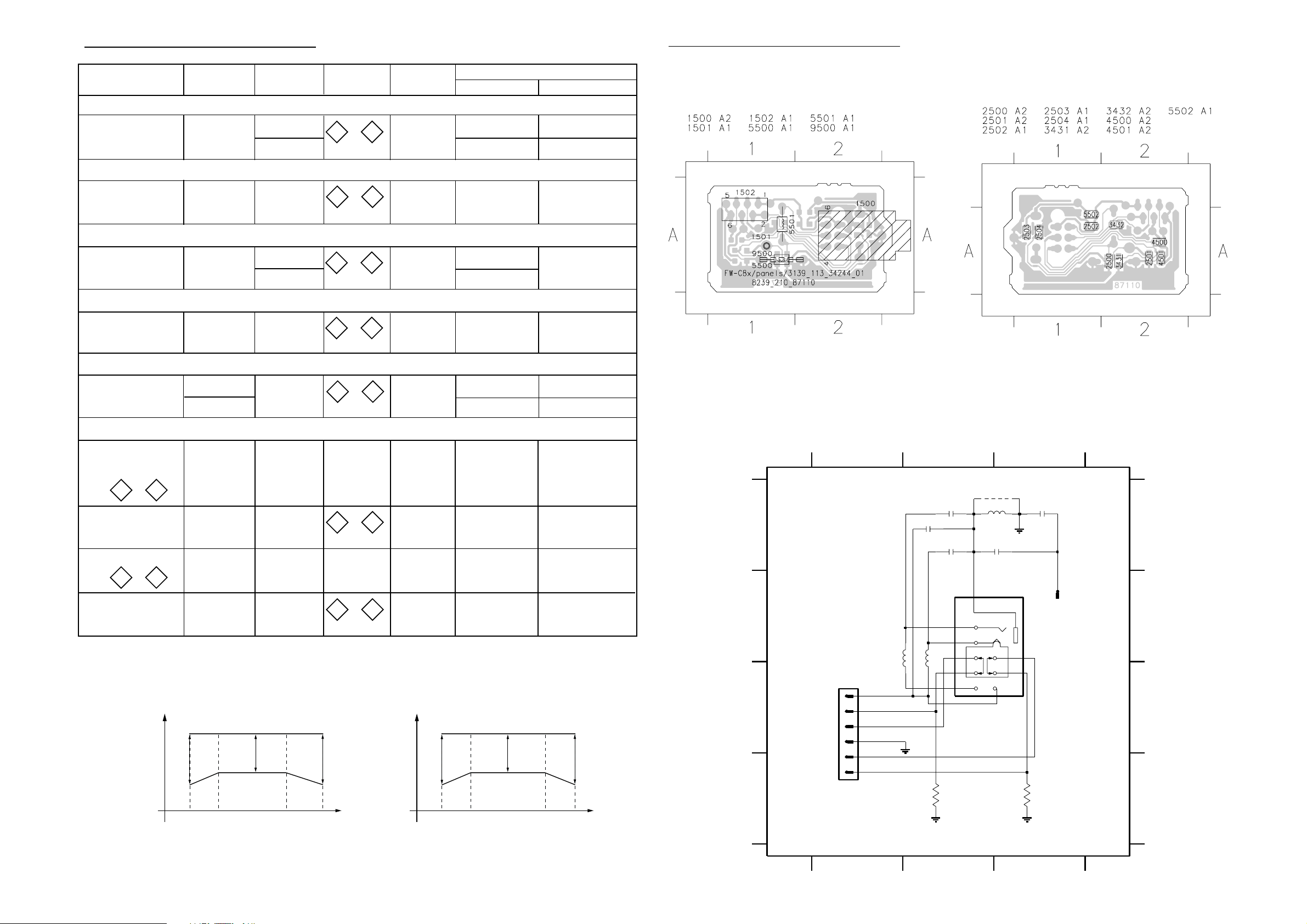
LAYOUT
This assembly drawing shows a summary of all possible versions.
For components used in a specific version see schematic diagram
and respective parts list.
3139 113 3424 pt4 dd wk0104
HEADPHONE PART - CIRCUIT DIAGRAM
1500 B2
1501 B3
1502 C1
2500 A2
2501 A3
2502 A2
2503 A2
2504 A3
123
Note : Some values may varies, see respective
parts list for correct value.
# : Provision
A
B
2u2
5501
a
C
FE-BT-VK-N
DPL_SW
Rhp
R
GNDa
L
Lhp
1502
1
2
3
4
5
6
2502
22n
5502
3431 D3
3432 D2
2500
22n
2503
100n
2u2
HEADPHONE BOARD - CHIP LAYOUTHEADPHONE BOARD - COMPONENT
This assembly drawing shows a summary of all possible versions.
For components used in a specific version see schematic diagram
and respective parts list.
3139 113 3424 pt4 dd wk0104
5500 A3
5501 B1
# 9500
5500
2u2
2504
100n
1500
9
7
8
4
5
6
3
TC38
5502 B2
9500 A3
# 2501
a
1
2
22n
A
1501
1
B
C
80
250
figure. 1
4k
12.5k
f(Hz)
100
250
figure. 2
4k
10k
f(Hz)
D
3432
a
330R
3139 118 53120...87110 for...3424 pt4 dd wk0104
3431
a
330R
123
D
 Loading...