

Color Television Chassis
FUZ2.0U
LA
32MF338B/27
I_17710_000.eps
040308
Contents Page Contents Page
1. Specifications 2
2. Operating Controls and Functions 6
3. Important Safety Precautions 8
4. Standard Notes for Servicing 12
5. Directions for Use 17
6. Cabinet Disassembly Instructions 18
7. Troubleshooting 24
8. Block Diagrams
System Control Block Diagram 31
Video Block Diagram 32
Audio-1 Block Diagram 33
Audio-2 Block Diagram 34
Digital Signal Process Block Diagram 35
Inverter Block Diagram 36
Power Supply Block Diagram 37
9. Circuit Diagrams & PWB Layouts 38
Power Supply 1/3 Parts Location Guide 39
Power Supply 1/3 Diagram 40
Power Supply 2/3 Diagram 41
Power Supply 2/3 Parts Location Guide 42
Power Supply 3/3 Parts Location Guide 43
Power Supply 3/3 & Side Jack Diagram 44
Power Supply Board Layout ( Top Side ) 45
Power Supply Board Layout ( Bottom Side ) 46
Power Supply Board Parts Location Guide 47
Side Jack Board Layout ( Top & Bottom Side ) 48
Side Jack Board Parts Location Guide 48
Inverter & Junction-B Diagram 49
Inverter Parts Location Guide 50
Inverter Board Layout ( Top Side ) 51
Junction-B Board Layout ( Top & Bottom Side ) 51
Inverter Board Layout ( Bottom Side ) 52
Inverter Board Parts Location Guide 53
Function Diagram 54
©
Copyright 2008 Philips Consumer Electronics B.V. Eindhoven, The Netherlands.
All rights reserved. No part of this publication may be reproduced, stored in a
retrieval system or transmitted, in any form or by any means, electronic,
mechanical, photocopying, or otherwise without the prior permission of Philips.
Function Diagram Parts Location Guide 54
Function Board Layout (Top & Bottom Side) 55
Function Board Parts Location Guide 55
IR Sensor & Junction-A Diagram 56
IR Sensor Diagram Parts Location Guide 56
IR Sensor Board Layout (Top & Bottom Side) 57
Junction-A Board Layout ( Top & Bottom Side ) 57
Digital Main 1/4 Diagram 58
Digital Main 2/4 Diagram 59
Digital Main 3/4 Diagram 60
Digital Main 4/4 Diagram 61
Digital Main Board Layout (Top Side) 62
Digital Main Board Layout (Bottom Side) 63
10. Waveforms 64
11. Wiring Diagram 65
12. Alignments 66
13. Abbreviations List 70
14. Structure & IC 73
15. Electrical Parts List 78
16. Mechanical Parts List 92
17. Revision List 93
Published by CS 0863 BU CD Consumer Care Printed in the Netherlands Subject to modification EN 3122 785 17710
2 FUZ2.0U LA
1. SPECIFICATIONS
1.1 Specifications
< TUNER / NTSC >
ANT. Input -----------------------75 Ω Unbal., F type
Description Condition Unit Nominal Limit
1. AFT Pull-in Range --- MHz ±2.3 ±2.1
20
20
23
2. Syncronizing Sens.
TV.ch.4
CA.ch.31
CA.ch.87
dBµ
dBµ
dBµ
---
---
---
< TUNER / ATSC >
Description Condition Unit Nominal Limit
1. Received Freq. Range (-28dBm) --- kHz --- ±100
-76/0
-76/0
-74/+4
2. ATSC Dynamic Range (min / max)
ch.4
ch.10
ch.41
dBm
dBm
dBm
---
---
---
< LCD PANEL >
Description Condition Unit Nominal Limit
1. Native Pixel Resolusion
2. Brightness --- cd/m
3. Viewing Angle
Horizontal
Ver ti ca l
Horizontal
Ver ti ca l
pixels
pixels
°
°
1366
768
2
320 ---
-88 to +88
-88 to +88
---
---
---
---
< VIDEO >
Description Condition Unit Nominal Limit
1. Over Scan
2. Color Temperature
3. Resolution (composite video)
Horizontal
Ver ti ca l
--x
y
Horizontal
Ver ti ca l
%
%
°K
---
---
line
line
5
5
12000
0.272
0.278
400
350
5±5
5±5
--±3%
±3%
---
---
< AUDIO >
All items are measured across 8 Ω load at speaker output terminal with L.P.F.
Description Condition Unit Nominal Limit
1. Audio Output Max Power
(ATSC 0dBfs)
2. Audio Distortion (NTSC) 500mW: Lch/Rch % 0.5/0.5 2.0/2.0
3. Audio Freq. Response (NTSC)
Note: Nominal specifications represent the design specifications. All units should be able to approximate these.
Some will exceed and some may drop slightly below these specifications. Limit specifications represent
the absolute worst condition that still might be considered acceptable. In no case should a unit fail to meet
limit specifications.
Lch/Rch W 10.0/10.0 9.0/9.0
-
6dB: Lch
-
6dB: Rch
Hz
Hz
70 to 10 k
70 to 10 k
---
---

< PICTURE / DISPLAY >
Description Specification
FUZ2.0U LA 3
1. Aspect ratio
2. Picture Enhancement
SOUND >
<
Description Specification
1. Output Power (RMS)
2. Sound Enhancement
3. Sound Mode
CONVENIENCE >
<
Description Specification
ON SCREEN DISPLAY LANGUAGE >
<
Description Specification
<
CONNECTIVITY >
Description Specification
Widescreen
Progressive Scan, 3D comb filter,
Smart Picture (4 models): Nature, Rich, Movie, Soft
2 x 10W
Mono, Stereo
Tr e bl e, B a s s
Auto Program, Closed Captioning Full Text, Sleeptimer
English, French, Spanish
1. Rear 75Ω / RF
COMPONENT 1- Component Video (YPbPr), Audio L/R input
COMPONENT 2- Component Video (YPbPr), Audio L/R input
VIDEO 1- Composite Video (Video In), S-Video, Audio L/R input
Coaxial digital audio output (Digital Only)
PC-VGA, Audio
HDMI 1, HDMI 2
2. Side Video 2- Composite Video (Video In), S-Video, Audio L/R input
<
WEIGHT & DIMENSIONS >
Description Specification
1. Weight (incl. Packaging):
2. Weight (excl. Packaging):
3. Carton Dimension
(W x H x D):
4. Product Dimension
(W x H x D):
<
POWER >
Description Specification
1. Power Consumption:
2. Standby Power Consumption:
3. Mains Power:
13.9 kg / 30.7 lbs
11 kg / 24.3 lbs
904 x 665 x 228 mm
35.6″ x 26.2″ x 9.0″
776 x 562 x 272 mm
30.6″ x 22.2″ x 10.7″
155W (Maximum)
< 1W
120V, 60Hz
4 FUZ2.0U LA
1.2 Technical Specifications
1.2.1 Technical Specifications
Panel : CMO
Active Area : 697.685mm(H) x
392.256mm(V)
Outline Dimension : 776.0mm(H) x 562.0mm(V) x
272.0mm(D)
Pixel Pitch : 0.17025mm(H) x
0.51075mm(V)
Pixel Format : 1366 x 768 (WXGA)
Color Depth : 8-bit, 16.7M colors
Luminance : 430 cd/m
Backlight : CCFL
Response Time : 8 msec.
Viewing Angle : 176/176 (L/R,U/D)
Contrast Ratio : 1500:1
Tuning system : PLL
CCFL MTBF : 40,000 hrs (min.)
Formats for PC : 800 x 600p 60Hz
(D-SUB 15pin) 1024 x 768p 60Hz
1280 x 768p 60Hz
1360 x 768p 60Hz
Formats for HDMI : 640 x 480p 60Hz
720 x 480i 30Hz (29.97Hz)
720 x 480p 60Hz (59.94Hz)
1920 x 1080i 30Hz (29.97Hz)
1280 x 720p 60Hz (59.94Hz)
Formats for : 720 x 480i 30Hz (29.97Hz)
Component 720 x 480p 60Hz (59.94Hz)
1920 x 1080i 30Hz (29.97Hz)
1280 x 720p 60Hz (59.94Hz)
Formats for S-in, : 720 x 480i 60Hz (59.94Hz)
NTSC & Video
Formats for ATSC : 640 x 480i 30Hz (29.97Hz)
640 x 480p 24Hz (23.976Hz)
640 x 480p 30Hz (29.97Hz)
640 x 480p 60Hz (59.94Hz)
704 x 480i 30Hz (29.97Hz)
704 x 480p 24Hz (23.976Hz)
704 x 480p 30Hz (29.97Hz)
704 x 480p 60Hz (59.94Hz)
1280 x 720p 24Hz (23.976Hz)
1280 x 720p
1280 x 720p
1920 x 1080i 30Hz (29.97Hz)
1920 x 1080p 24Hz (23.976Hz)
1920 x 1080p
1.2.2 Sound
Sound systems : Mono / Stereo / Sap
Maximum power : 2 x 10W
2
30Hz (29.97Hz)
60Hz (59.94Hz)
30Hz (29.97Hz)
1.2.3 Miscellaneous
Power supply
AC-input : 120V AC, 60Hz
Normal Operation
Power Consumption : < 155W
Standby power : < 1W
Power cord length : 1545 mm (min.)
Power cord type : NISPT-2
Power indicator : LED (On: Green, Standby:
Red)
Ambient conditions
Temperature : 0 to 50 °C
Humidity :
Power consumption
Normal Operation : < 155W
Standby power : < 1W
≦80%RH
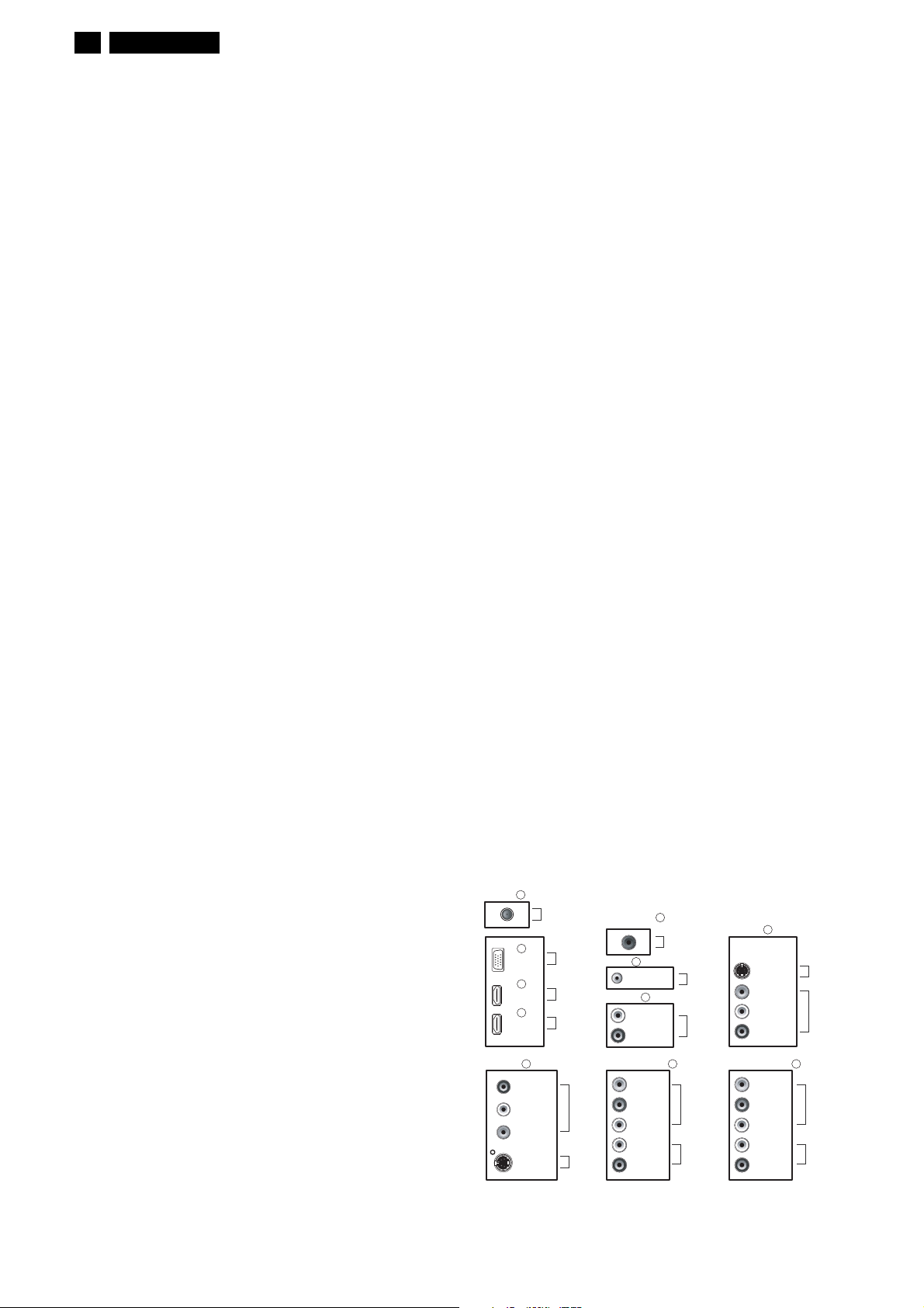
1.3 Connections
1.3.1 Signal Connector
(1)Tuner : NTSC / ATSC.
(2)D-SUB : VGA input (D-SUB 15 pins).
(3)HDMI 1 : HDMI 1 input with HDMI-IN audio
R/L.
(4)HDMI 2 : HDMI 2 input.
(5)DIGITAL AUDIO OUT :RCA jack.
(6)PC-IN Audio : Mini-jack.
(7)HDMI-IN Audio : Audio R/L (RCA jack) for
HDMI(DVI).
(8)VIDEO 1 : Video 1 (CVBS, RCA jack) and S-
Video 1 share with same audio R/
L (RCA jack).
(9)VIDEO 2 : Video 2 (CVBS, RCA jack) and S-
Video 2 share with same audio R/
L (RCA jack).
(10)COMPONENT 1 : Y/Pb/Pr component video1
(RCA jack) with audio R/L (RCA
jack).
(11)COMPONENT 2 : Y/Pb/Pr component video2
(RCA jack) with audio R/L (RCA
jack).
1
TUNER
TU1
2
D-SUB
3
HDMI 1
4
HDMI 2
9 10 11
VIDEO 2
AUDIO-R
AUDIO-L
VIDEO
S-VIDEO
JK3701
JK4001
JK4002
JK752
JK751
DIGITAL
AUDIO OUT
(COAXIAL)
6
PC-IN
AUDIO
HDMI-IN
AUDIO-L
AUDIO-R
Y
Pb
Pr
AUDIO-L
AUDIO-R
5
JK7515
JK7501
7
JK7705
JK7711
JK7712
VIDEO 1
COMPONENT 2COMPONENT 1
8
S-VIDEO
VIDEO
AUDIO-L
AUDIO-R
Y
Pb
Pr
AUDIO-L
AUDIO-R
JK7701
JK7702
JK7713
JK7714

FUZ2.0U LA 5
0
1.3.2 Input Signal
TV Signal type
RF Signal : Aerial input / 10mV(80dBuV)
Video signal : Video (RCA CVBS input) / 1Vpp
(300mV-sync, 700mV-video.)
S video input / 1VppY-signal,
300mVpp C-signal
COMPONENT Video (Y/Pb/Pr
input) / 1Vpp Y signal, 350mVpp Pb,
Pr signal
HDMI : Digital interface with 4 channels
TMDS signal
Audio signal :
Audio R/L for COMPONET 1.
Level :- Nominal : 0.5 V rms.
- Maximum : 1.5 V rms.
- Impedance > 10 k Ω.
Audio R/L for COMPONET 2.
Level :- Nominal : 0.5 V rms.
- Maximum : 1.5 V rms.
- Impedance > 10 k Ω.
Audio R/L for VIDEO 1.
Level :- Nominal : 0.5 V rms.
- Maximum : 1.5 V rms.
- Impedance > 10 k Ω.
Audio R/L for VIDEO 2.
Level :- Nominal : 0.5 V rms.
- Maximum : 1.5 V rms.
- Impedance > 10 k Ω.
Audio R/L for HDMI-IN.
Level :- Nominal : 0.5 V rms.
- Maximum : 1.5 V rms.
- Impedance > 10 k Ω.
PC Signal type
Analog Video : 0.7 Vp-p linear, positive polarity
Separate Sync.: TTL level, separate, positive or
negative polarity
Audio signal : Mini-jack audio input,
Level: - Nominal : 0.5 V rms.
- Maximum : 1.5 V rms.
- Impedance > 10 k Ω.
Digital Audio output : 0.5 V ~ 1 V Square Wave.
1.3.3 HDMI Pin assignment
Type A Connector
No.1
No.19
PIN No. SIGNAL
8 TMDS Data0 shield
9 TMDS Data0-
10 TMDS Clock+
11 TMDS Clock shield
12 TMDS Clock-
13 CEC
14 Reserved (N.C. on device)
15 SCL
16 SDA
17 DDC/CEC Ground
18 +5V Power
19 Hot Plug Detect
1.3.4 VGA Pin assignmentnput
1
6
11
PIN No. SIGNAL
1Red
2Green
3Blue
4GND
5Self test
6 Red GND
7 Green GND
8 Blue GND
9 +5V (Supply from PC)
10 Sync GND
11 GND
12 Bi-directional data (SDA)
5
1
15
No.18No.2
PIN No. SIGNAL
1TMDS Data2+
2TMDS Data2 shield
3TMDS Data2-
4TMDS Data1+
5TMDS Data1 shield
6TMDS Data1-
7TMDS Data0+
13 H-sync
14 V-sync
15 Data clock (SCL)
6 FUZ2.0U LA
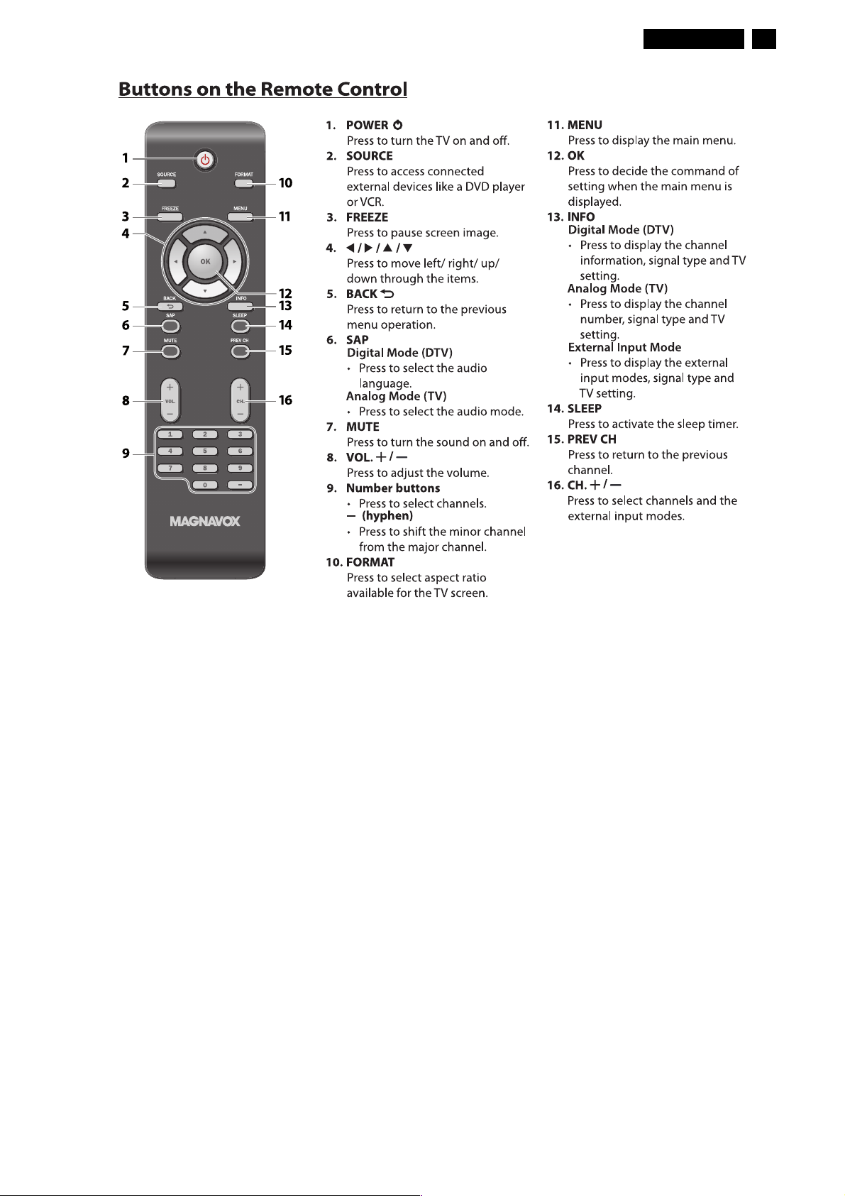
2. OPERATING CONTROLS AND FUNCTIONS
FUZ2.0U LA 7
8 FUZ2.0U LA
3. IMPORTANT SAFETY PRECAUTIONS
Prior to shipment from the factory, our products are strictly inspected for recognized product safety and electrical
codes of the countries in which they are to be sold. However, in order to maintain such compliance, it is equally
important to implement the following precautions when a set is being serviced.
Safety Precautions for LCD TV
Circuit
1. Before returning an instrument to the
customer, always make a safety check of the
entire instrument, including, but not limited to, the
following items:
a. Be sure that no built-in protective devices are
defective and have been defeated during
servicing. (1) Protective shields are provided
on this chassis to protect both the technician
and the customer. Correctly replace all missing
protective shields, including any removed for
servicing convenience. (2) When reinstalling
the chassis and/or other assembly in the
cabinet, be sure to put back in place all
protective devices, including but not limited to,
nonmetallic control knobs, insulating
fishpapers, adjustment and compartment
covers/shields, and isolation resistor/capacitor
networks. Do not operate this instrument or
permit it to be operated without all
protective devices correctly installed and
functioning. Servicers who defeat safety
features or fail to perform safety checks
may be liable for any resulting damage.
b. Be sure that there are no cabinet openings
through which an adult or child might be able to
insert their fingers and contact a hazardous
voltage. Such openings include, but are not
limited to, (1) spacing between the Liquid
Crystal Panel and the cabinet mask, (2)
excessively wide cabinet ventilation slots, and
(3) an improperly fitted and/or incorrectly
secured cabinet back cover.
c. Antenna Cold Check - With the instrument AC
plug removed from any AC source, connect an
electrical jumper across the two AC plug
prongs. Place the instrument AC switch in the
on position. Connect one lead of an ohmmeter
to the AC plug prongs tied together and touch
the other ohmmeter lead in turn to each tuner
antenna input exposed terminal screw and, if
applicable, to the coaxial connector. If the
measured resistance is less than 1.0 megohm
or greater than 5.2 megohm, an abnormality
exists that must be corrected before the
instrument is returned to the customer. Repeat
this test with the instrument AC switch in the off
position.
d. Leakage Current Hot Check - With the
instrument completely reassembled, plug the
AC line cord directly into a 120 V AC outlet. (Do
not use an isolation transformer during this
test.) Use a leakage current tester or a
metering system that complies with American
National Standards Institute (ANSI) C101.1
Leakage Current for Appliances and
Underwriters Laboratories (UL) 1410, (50.7).
With the instrument AC switch first in the on
position and then in the off position, measure
from a known earth ground (metal water pipe,
conduit, etc.) to all exposed metal parts of the
instrument (antennas, handle brackets, metal
cabinet, screw heads, metallic overlays, control
shafts, etc.), especially any exposed metal
parts that offer an electrical return path to the
chassis. Any current measured must not
exceed 0.5 milli-ampere. Reverse the
instrument power cord plug in the outlet and
repeat the test.
READING SHOULD
NOT BE ABOVE 0.5 mA
LEAKAGE
DEVICE
BEING
TESTED
TEST ALL EXPOSED
METAL SURFACES
ALSO TEST WITH
PLUG REVERSED
USING AC
ADAPTER PLUG
AS REQUIRED
ANY MEASUREMENTS NOT WITHIN THE
LIMITS SPECIFIED HEREIN INDICATE A
POTENTIAL SHOCK HAZARD THAT MUST
BE ELIMINATED BEFORE RETURNING THE
INSTRUMENT TO THE CUSTOMER OR
BEFORE CONNECTING THE ANTENNA OR
ACCESSORIES.
2. Read and comply with all caution and safety-
related notes on or inside the receiver cabinet, on
the receiver chassis, or on the Liquid Crystal
Panel.
3. Design Alteration Warning - Do not alter or add
to the mechanical or electrical design of this TV
receiver. Design alterations and additions,
including, but not limited to circuit modifications
and the addition of items such as auxiliary audio
and/or video output connections, might alter the
safety characteristics of this receiver and create a
hazard to the user. Any design alterations or
additions will void the manufacturer's warranty and
may make you, the servicer, responsible for
CURRENT
TESTER
+
EARTH
GROUND
_

FUZ2.0U LA 9
personal injury or property damage resulting
therefrom.
4. Hot Chassis Warning -
a. Some TV receiver chassis are electrically
connected directly to one conductor of the AC
power cord and maybe safety-serviced without
an isolation transformer only if the AC power
plug is inserted so that the chassis is
connected to the ground side of the AC power
source. To confirm that the AC power plug is
inserted correctly, with an AC voltmeter,
measure between the chassis and a known
earth ground. If a voltage reading in excess of
1.0 V is obtained, remove and reinsert the AC
power plug in the opposite polarity and again
measure the voltage potential between the
chassis and a known earth ground.
b. Some TV receiver chassis normally have 85V
AC(RMS) between chassis and earth ground
regardless of the AC plug polarity. This chassis
can be safety-serviced only with an isolation
transformer inserted in the power line between
the receiver and the AC power source, for both
personnel and test equipment protection.
c. Some TV receiver chassis have a secondary
ground system in addition to the main chassis
ground. This secondary ground system is not
isolated from the AC power line. The two
ground systems are electrically separated by
insulation material that must not be defeated or
altered.
5. Observe original lead dress. Take extra care to
assure correct lead dress in the following areas: a.
near sharp edges, b. near thermally hot parts-be
sure that leads and components do not touch
thermally hot parts, c. the AC supply, d. high
voltage, and, e. antenna wiring. Always inspect in
all areas for pinched, out of place, or frayed wiring.
Check AC power cord for damage.
6. Components, parts, and/or wiring that appear to
have overheated or are otherwise damaged
should be replaced with components, parts, or
wiring that meet original specifications.
Additionally, determine the cause of overheating
and/or damage and, if necessary, take corrective
action to remove any potential safety hazard.
7. Product Safety Notice - Some electrical and
mechanical parts have special safety-related
characteristics which are often not evident from
visual inspection, nor can the protection they give
necessarily be obtained by replacing them with
components rated for higher voltage, wattage, etc.
Parts that have special safety characteristics are
identified by a # on schematics and in parts lists.
Use of a substitute replacement that does not
have the same safety characteristics as the
recommended replacement part might create
shock, fire, and/or other hazards. The product's
safety is under review continuously and new
instructions are issued whenever appropriate.
Prior to shipment from the factory, our products
are strictly inspected to confirm they comply with
the recognized product safety and electrical codes
of the countries in which they are to be sold.
However, in order to maintain such compliance, it
is equally important to implement the following
precautions when a set is being serviced.

10 FUZ2.0U LA
Precautions during Servicing
A. Parts identified by the # symbol are critical for
safety.
Replace only with part number specified.
B. In addition to safety, other parts and assemblies
are specified for conformance with regulations
applying to spurious radiation. These must also be
replaced only with specified replacements.
Examples: RF converters, RF cables, noise
blocking capacitors, and noise blocking filters, etc.
C. Use specified internal wiring. Note especially:
1) Wires covered with PVC tubing
2) Double insulated wires
3) High voltage leads
D. Use specified insulating materials for hazardous
live parts. Note especially:
1) Insulation Tape
2) PVC tubing
3) Spacers
4) Insulators for transistors.
E. When replacing AC primary side components
(transformers, power cord, etc.), wrap ends of
wires securely about the terminals before
soldering.
F. Observe that the wires do not contact heat
producing parts (heat sinks, oxide metal film
resistors, fusible resistors, etc.)
G. Check that replaced wires do not contact sharp
edged or pointed parts.
H. When a power cord has been replaced, check that
5~6 kg of force in any direction will not loosen it.
I. Also check areas surrounding repaired locations.
J. Use care that foreign objects (screws, solder
droplets, etc.) do not remain inside the set.
K. When connecting or disconnecting the internal
connectors, first, disconnect the AC plug from the
AC supply outlet.
L. When installing parts or assembling the cabinet
parts, be sure to use the proper screws and
tighten certainly.

FUZ2.0U LA 11
Safety Check after Servicing
Examine the area surrounding the repaired location for damage or deterioration. Observe that screws, parts and
wires have been returned to original positions. Afterwards, perform the following tests and confirm the specified
values in order to verify compliance with safety standards.
1. Clearance Distance
When replacing primary circuit components, confirm
specified clearance distance (d) and (d') between
soldered terminals, and between terminals and
surrounding metallic parts. (See Fig. 1)
Table 1: Ratings for selected area
Chassis or Secondary Conductor
Primary Circuit
AC Line Voltage Region
110 to 130 V
Note: This table is unofficial and for reference only. Be
sure to confirm the precise values.
U.S.A. or
Canada
Clearance
Distance (d), (d’)
≥ 3.2 mm
(0.126 inches)
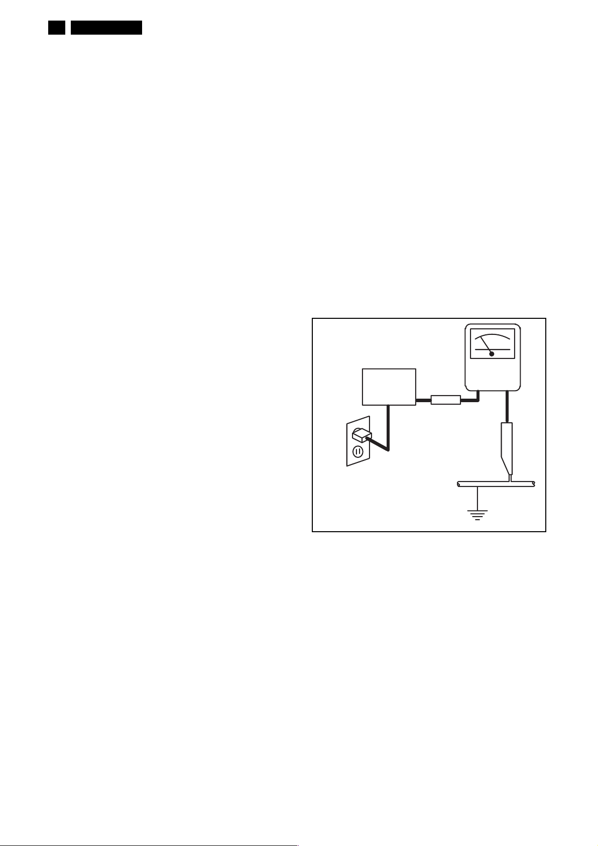
2. Leakage Current Test
Confirm the specified (or lower) leakage current
between B (earth ground, power cord plug prongs) and
externally exposed accessible parts (RF terminals,
antenna terminals, video and audio input and output
terminals, microphone jacks, earphone jacks, etc.) is
lower than or equal to the specified value in the table
below.
Measuring Method: (Power ON)
Insert load Z between B (earth ground, power cord plug
prongs) and exposed accessible parts. Use an AC
voltmeter to measure across both terminals of load Z.
See Fig. 2 and following table.
d' d
Fig. 1
Exposed Accessible Part
Z
AC Voltmeter
(High Impedance)
Earth Ground
B
Power Cord Plug Prongs
Fig. 2
Table 2: Leakage current ratings for selected areas
AC Line Voltage Region Load Z Leakage Current (i) Earth Ground (B) to:
110 to 130 V
Note: This table is unofficial and for reference only. Be sure to confirm the precise values.
U.S.A. or
Canada
0.15 µF CAP. & 1.5 kΩ
RES. Connected in parallel
i ≤ 0.5 mA rms
Exposed accessible
parts
12 FUZ2.0U LA
4. STANDARD NOTES FOR SERVICING
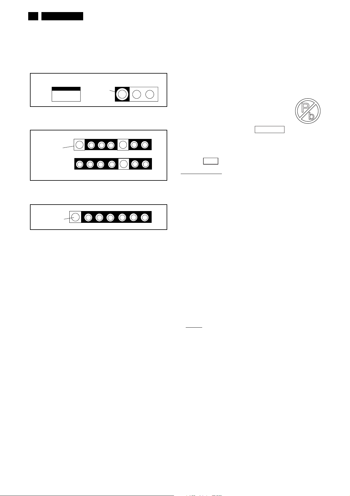
Circuit Board Indications
1. The output pin of the 3 pin Regulator ICs is
indicated as shown.
Top View
Out
2. For other ICs, pin 1 and every fifth pin are
indicated as shown.
Pin 1
3. The 1st pin of every male connector is indicated as
shown.
Pin 1
Input
In
Bottom View
5
10
Pb (Lead) Free Solder
When soldering, be sure to use the Pb free solder.
Information about lead-free soldering
Philips CE is producing lead-free sets from 1.1.2005
onwards.
IDENTIFICATION
Regardless of special logo (not always
indicated)
One must treat all sets from
onwards, according to the next rule:
Serial Number gives a 14-digit. Digit 5&6 shows the
YEAR, and digit 7&8 shows the WEEK.
So from onwards=from 1 Jan 2005 onwards
Important note
must be treated in this way as long as you avoid
mixing solder-alloys (leaded/ lead-free). So best to
always use SAC305 and the higher temperatures
belong to this.
Due to lead-free technology some rules have to be
respected by the workshop during a repair:
• Use only lead-free solder alloy Philips SAC305 with
order code 0622 149 00106. If lead-free solderpaste is required, please contact the manufacturer
of your solder-equipment. In general use of solderpaste within workshops should be avoided because
paste is not easy to store and to handle.
• Use only adequate solder tools applicable for lead-
free solder alloy. The solder tool must be able
• To reach at least a solder-temperature of 400°C,
• To stabilize the adjusted temperature at the solder-
• To exchange solder-tips for different applications.
• Adjust your solder tool so that a temperature around
360°C
solder joint. Heating-time of the solder-joint should
not exceed ~ 4 sec. Avoid temperatures above
400°C otherwise wear-out of tips will rise drastically
and flux-fluid will be destroyed. To avoid wear-out of
tips switch off un-used equipment, or reduce heat.
0501
: In fact also products of year 2004
tip
- 380°C is reached and stabilized at the
1 Jan 2005

FUZ2.0U LA 13
• Mix of lead-free solder alloy / parts with leaded
solder alloy / parts is possible but PHILIPS
recommends strongly to avoid mixed solder alloy
types (leaded and lead-free).
If one cannot avoid or does not know whether
product is lead-free, clean carefully the solder-joint
from old solder alloy and re-solder with new solder
alloy (SAC305).
• Use only original spare-parts listed in the Service-
Manuals. Not listed standard-material (commodities)
has to be purchased at external companies.
• Special information for BGA-ICs:
- always use the 12nc-recognizable soldering
temperature profile of the specific BGA (for desoldering always use the lead-free temperature
profile, in case of doubt)
- lead free BGA-ICs will be delivered in so-called
'dry-packaging' (sealed pack including a silica gel
pack) to protect the IC against moisture. After
opening, dependent of MSL-level seen on indicatorlabel in the bag, the BGA-IC possibly still has to be
baked dry. (MSL=Moisture Sensitivity Level). This
will be communicated via AYS-website.
Do not re-use BGAs at all.
• For sets produced before 1.1.2005 (except products
of 2004), containing leaded solder-alloy and
components, all needed spare-parts will be available
till the end of the service-period. For repair of such
sets nothing changes.
Alternative BOM Identification
In September 2003, Philips CE introduced a change in
the way the serial number is composed. from this data
on, the third digit in the serial number (example:
AG2B0335000001) indicates the number of the
alternative BOM (Bill of Materials used for producing
the specific model of TV set). It is possible that the
same TV model on the market is produced with e.g.
two different types of displays, coming from two
different O.E.M.s. By looking at the third digit of the
serial number, the service technician can see if there
is more than one type of B.O.M. used in the production
of the TV set he is working with. He can then consult
the At Your Service Web site, where he can type in the
Commercial Type Version Number of the TV set (e.g.
28PW9515/12), after which a screen will appear that
gives infomation about the number of alternative
B.O.M.s used. If the third digit of the serial number
contains the number 1 (example: AG1B033500001),
then there is only one B.O.M. version of the TV set on
the market. If the third digit is a 2 (example:
AG2B0335000001), then there are two different
B.O.M.s. Information about this is important for
ordering the correct spare parts! For the third digit, the
numbers 1...9 and the characters A...Z can be used,
so in total: 9 plus 26 = 35 different B.O.M.s can be
indicated by the third digit of the serial number.
For additional questions please contact your local
repair-helpdesk.
14 FUZ2.0U LA
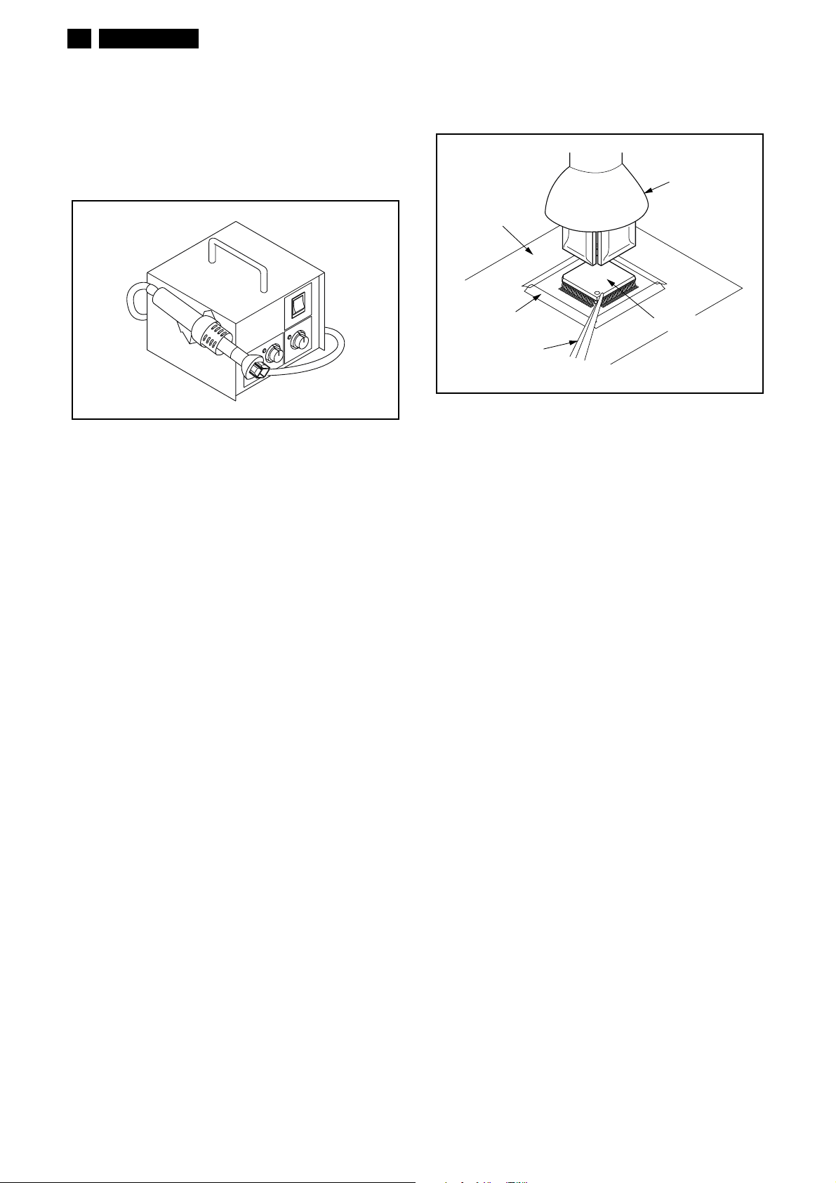
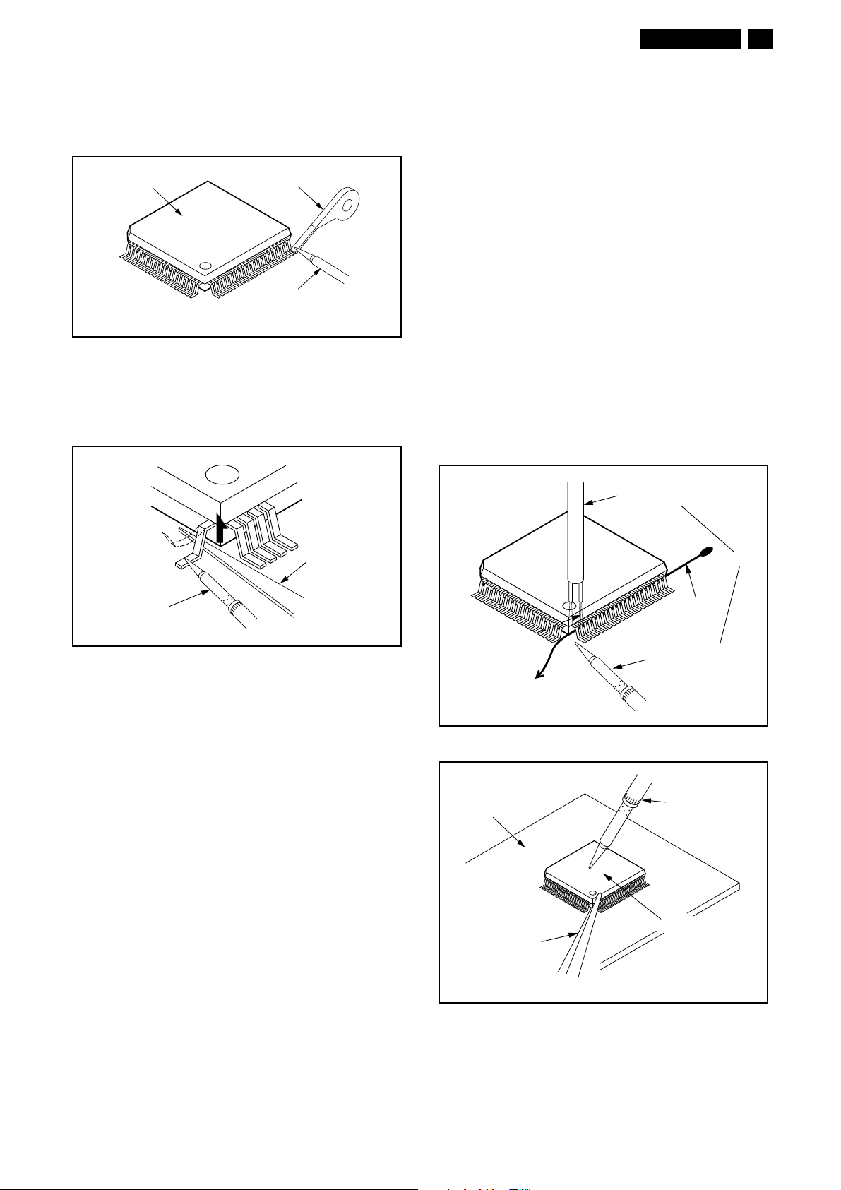
How to Remove / Install Flat Pack-IC
1. Removal
With Hot-Air Flat Pack-IC Desoldering Machine:
1. Prepare the hot-air flat pack-IC desoldering
machine, then apply hot air to the Flat Pack-IC
(about 5 to 6 seconds). (Fig. S-1-1)
Fig. S-1-1
2. Remove the flat pack-IC with tweezers while
applying the hot air.
3. Bottom of the flat pack-IC is fixed with glue to the
CBA; when removing entire flat pack-IC, first apply
soldering iron to center of the flat pack-IC and heat
up. Then remove (glue will be melted). (Fig. S-1-6)
4. Release the flat pack-IC from the CBA using
tweezers. (Fig. S-1-6)
3. The flat pack-IC on the CBA is affixed with glue, so
be careful not to break or damage the foil of each
pin or the solder lands under the IC when
removing it.
Hot-air
Flat Pack-IC
Desoldering
CBA
Masking
Tape
Tweezers
Machine
Flat Pack-IC
Fig. S-1-2
CAUTION:
1. The Flat Pack-IC shape may differ by models. Use
an appropriate hot-air flat pack-IC desoldering
machine, whose shape matches that of the Flat
Pack-IC.
2. Do not supply hot air to the chip parts around the
flat pack-IC for over 6 seconds because damage
to the chip parts may occur. Put masking tape
around the flat pack-IC to protect other parts from
damage. (Fig. S-1-2)
FUZ2.0U LA 15
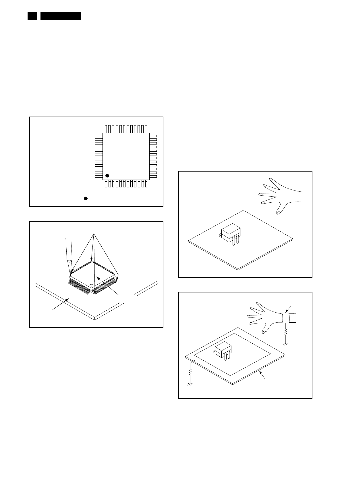
With Soldering Iron:
1. Using desoldering braid, remove the solder from
all pins of the flat pack-IC. When you use solder
flux which is applied to all pins of the flat pack-IC,
you can remove it easily. (Fig. S-1-3)
Flat Pack-IC
Desoldering Braid
Soldering Iron
Fig. S-1-3
2. Lift each lead of the flat pack-IC upward one by
one, using a sharp pin or wire to which solder will
not adhere (iron wire). When heating the pins, use
a fine tip soldering iron or a hot air desoldering
machine. (Fig. S-1-4)
With Iron Wire:
1. Using desoldering braid, remove the solder from
all pins of the flat pack-IC. When you use solder
flux which is applied to all pins of the flat pack-IC,
you can remove it easily. (Fig. S-1-3)
2. Affix the wire to a workbench or solid mounting
point, as shown in Fig. S-1-5.
3. While heating the pins using a fine tip soldering
iron or hot air blower, pull up the wire as the solder
melts so as to lift the IC leads from the CBA
contact pads as shown in Fig. S-1-5.
4. Bottom of the flat pack-IC is fixed with glue to the
CBA; when removing entire flat pack-IC, first apply
soldering iron to center of the flat pack-IC and heat
up. Then remove (glue will be melted). (Fig. S-1-6)
5. Release the flat pack-IC from the CBA using
tweezers. (Fig. S-1-6)
Note: When using a soldering iron, care must be
taken to ensure that the flat pack-IC is not
being held by glue. When the flat pack-IC is
removed from the CBA, handle it gently
because it may be damaged if force is applied.
Sharp
Pin
Fine Tip
Soldering Iron
3. Bottom of the flat pack-IC is fixed with glue to the
CBA; when removing entire flat pack-IC, first apply
soldering iron to center of the flat pack-IC and heat
up. Then remove (glue will be melted). (Fig. S-1-6)
4. Release the flat pack-IC from the CBA using
tweezers. (Fig. S-1-6)
Fig. S-1-4
To Solid
Mounting Point
CBA
Hot Air Blower
or
Iron Wire
Soldering Iron
Fig. S-1-5
Fine Tip
Soldering Iron
Tweezers
Flat Pack-IC
Fig. S-1-6
16 FUZ2.0U LA
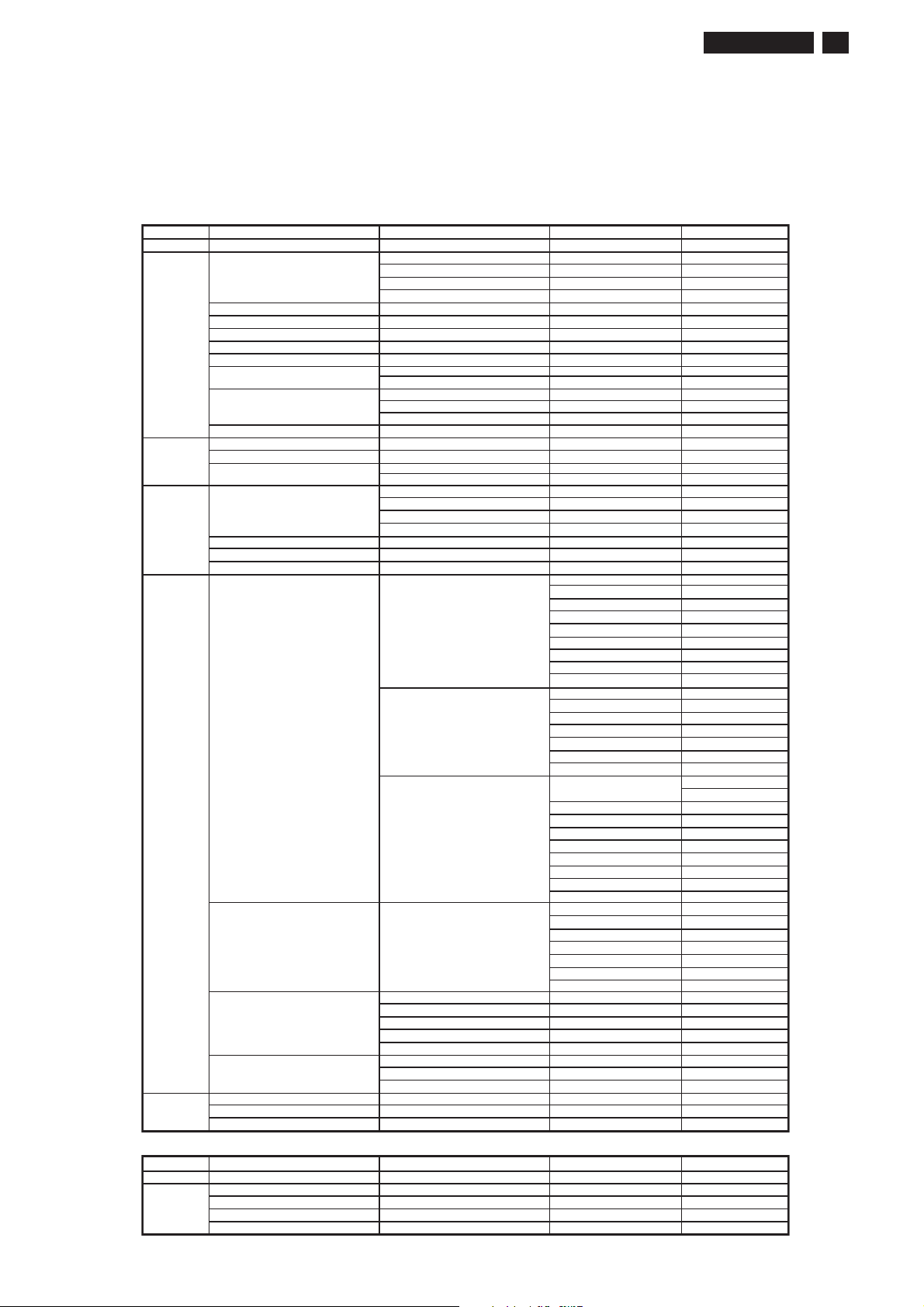
2. Installation
1. Using desoldering braid, remove the solder from
the foil of each pin of the flat pack-IC on the CBA
so you can install a replacement flat pack-IC more
easily.
2. The “●” mark on the flat pack-IC indicates pin 1.
(See Fig. S-1-7.) Be sure this mark matches the 1
on the PCB when positioning for installation. Then
presolder the four corners of the flat pack-IC. (See
Fig. S-1-8.)
3. Solder all pins of the flat pack-IC. Be sure that
none of the pins have solder bridges.
Example :
Pin 1 of the Flat Pack-IC
is indicated by a " " mark.
Fig. S-1-7
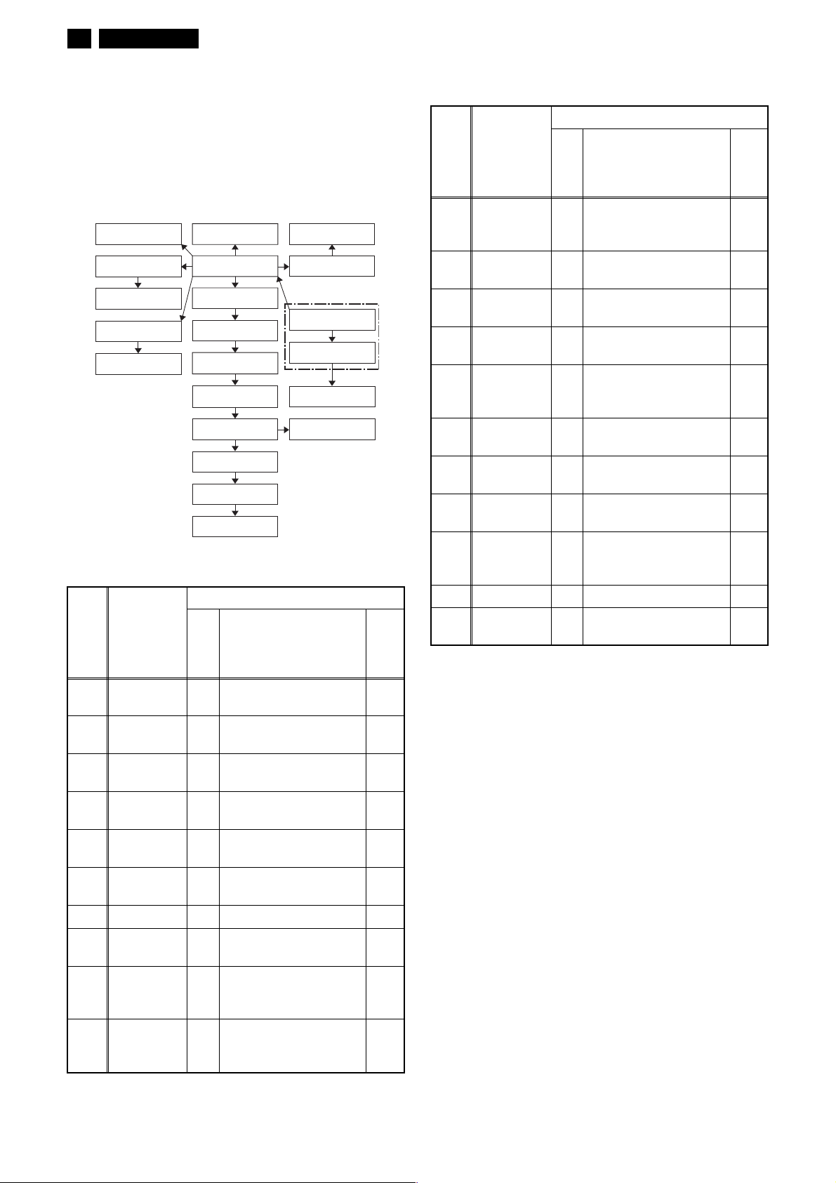
Instructions for Handling Semiconductors
Electrostatic breakdown of the semi-conductors may
occur due to a potential difference caused by
electrostatic charge during unpacking or repair work.
1. Ground for Human Body
Be sure to wear a grounding band (1 MΩ) that is
properly grounded to remove any static electricity that
may be charged on the body.
2. Ground for Workbench
Be sure to place a conductive sheet or copper plate
with proper grounding (1 MΩ) on the workbench or
other surface, where the semi-conductors are to be
placed. Because the static electricity charge on
clothing will not escape through the body grounding
band, be careful to avoid contacting semi-conductors
with your clothing.
<Incorrect>
CBA
Presolder
Flat Pack-IC
Fig. S-1-8
<Correct>
1MΩ
CBA
Grounding Band
1MΩ
CBA
Conductive Sheet or
Copper Plate
5. Directions for Use
You can download this infomation from the following website:
http://www.philips.com/support
http://www.p4c.philips.com
OSD Menu list
Menu Label
EXIT
Picture
Setup
Features
Language English
Smart Picture
Reset Picture Setting
Color temperature Cool
Energy Saving slider
Reset Sound Setting
Channel List
Manual Register
Antenna
Closed Caption
PC Settings
HDMI1 Audio Auto
Español
Français
Live TV Label
Picture Mode
Movie expand Movie expand
Nature
Rich
Movie
Soft
redilsssenthgirB
redilstsartnoC
redilsroloC
redilstniT
redilsssenprahS
Off
Reset to default
Normal
Warm
redilselberTdnuoS
redilsssaB
Off
Reset to default
kcaBmargorpotuA
Air
Analog Cable
Auto
Conventional CC Off
Auto Adjustment slider
Horizontal Position slider
Vertical Position slider
Digital
Analog
langis 9:61 roflangis 3:4 rof
lamroNlamroN
mooZ9:61
ediWediW
FUZ2.0U LA 17
reyaL ht5reyaL ht4reyaL dr3reyaL dn2reyaL ts1
CC-1
CC-2
CC-3
CC-4
T-1
T-2
T-3
T-4
ffOCC VTD
CS-1
CS-2
CS-3
CS-4
CS-5
CS-6
nOgnitteS resUelytS CC
Off
Font Style
Font Size
Font Color
Font Opacity
Back Color
Back Opacity
Edge Color
Edge Type
kcol sgnitar eivoM SUniP retnElortnoC latneraP
US TV ratings lock
Canadian English Rating
Canadian French Rating
Region ratings lock
Clear Regions lock
Change Pin
redilskcolC
redilsesahP
reyaL ht5reyaL ht4reyaL dr3reyaL dn2reyaL ts1
18 FUZ2.0U LA
6. CABINET DISASSEMBLY INSTRUCTIONS
1. Disassembly Flowchart
This flowchart indicates the disassembly steps for the
cabinet parts, and the Board in order to gain access to
item(s) to be serviced. When reassembling, follow the
steps in reverse order. Bend, route and dress the
cables as they were.
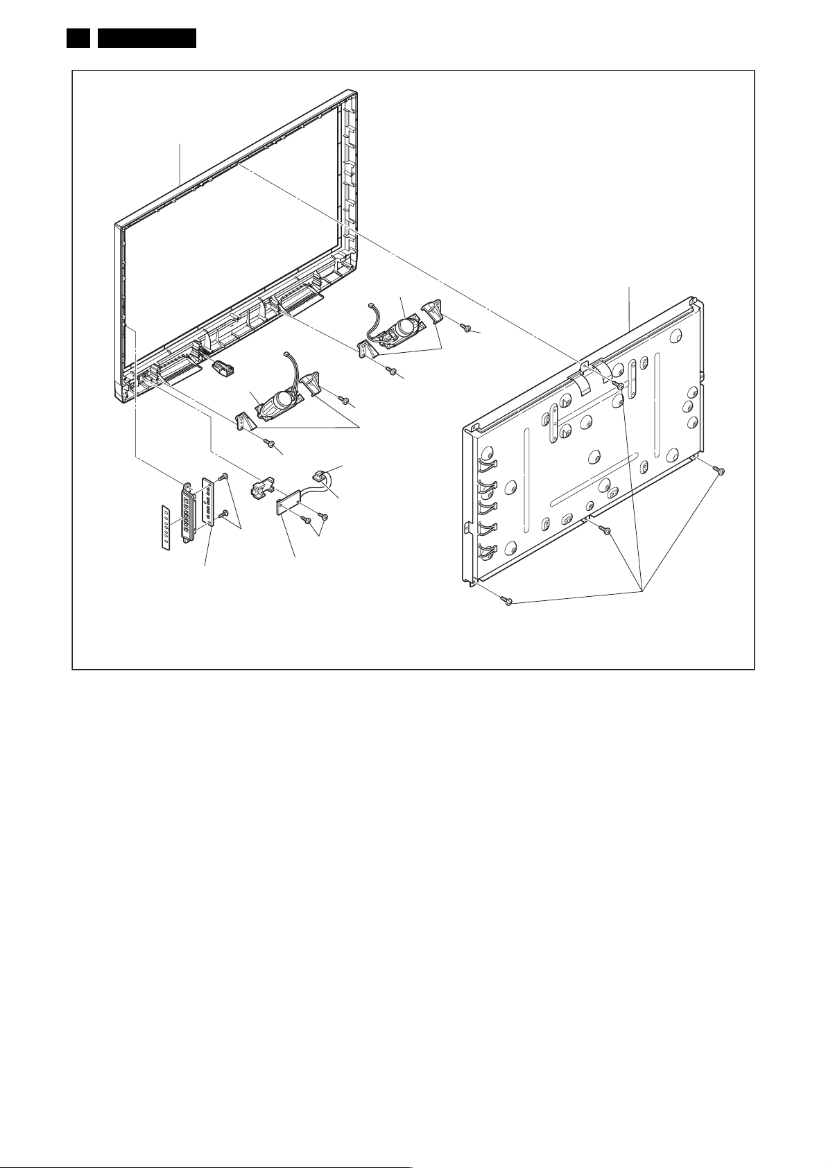
[18] Function Board
[19] Speaker
Holder (L,R)
[20] Speaker(s)
[16] Junction-A
Board
[17] IR Sensor
Board
[14] Stand Holder
[4] Rear Cabinet
[7] Shield (T)
[8] Shield Box
[9] Digital Main
Board Unit
[10] Power Supply
Board
[11] Inverter Board
[13] PCB Holder
(L,R)
[15] LCD Module
Assembly
[21] Front Cabinet
[6] Side Jack Board
[5] Jack Holder (A)
Stand Assembly
[1] Stand Base
Plate
[2] Stand Cover
[3] Stand Hinge
[12] Junction-B
Board
2. Disassembly Method
Removal
Step/
Loc.
Part
No.
Stand Base
[1]
Plate
Stand
[2]
Cover
Stand
[3]
Hinge
Rear
[4]
Cabinet
Jack Holder
[5]
(A)
Side Jack
[6]
Board
[7] Shield (T) D2 (S-9), (S-10), (N-1) ---
[8] Shield Box D2
Digital Main
[9]
Board UnitD2D5
Power
[10]
Supply
Board
Remove/*Unhook/
Fig.
No.
Unlock/Release/
Unplug/Unclamp/
Note
Desolder
D1 4(S-1), 3(S-2), 4(S-3) ---
D1 --------------- ---
D1 --------------- ---
D1 12(S-4), (S-5), 2(S-6) ---
D2 (S-7) ---
D2
2(S-8), *CN751 ---
D5
2(S-11), 2(S-12),
3(S-13), 4(S-14)
*CN3601, *CN3701,
*CN3704, *CN4501,
*CN4502
7(S-15), *CN102,
D2
*CN501, *CN801,
D5
*CN802, *CN1901
---
---
---
Removal
Step/
Loc.
No.
Part
Remove/*Unhook/
Fig.
No.
Unlock/Release/
Unplug/Unclamp/
Note
Desolder
7(S-16), *CN1050,
D3
*CN1100, *CN1150,
D5
*CN1200, *CN1250
D3
Desolder ---
D5
---
D3 4(S-17) ---
D3 2(S-18), 2(S-19) ---
[11]
[12]
[13]
[14]
Inverter
Board
Junction-B
Board
PCB Holder
(L,R)
Stand
Holder
LCD
[15]
Module
D4 4(S-20) ---
Assembly
[16]
[17]
[18]
Junction-A
Board
IR Sensor
Board
Function
Board
D4
Desolder ---
D5
D4
2(S-21), *CL102A ---
D5
D4
2(S-22) ---
D5
Speaker
[19]
Holder
D4 4(S-23) ---
(L,R)
[20] Speaker(s) D4 --------------- ---
Front
[21]
↓
(1)
Cabinet
↓
(2)
D4 --------------- ---
↓
(3)
↓
(4)
↓
(5)
Note:
(1) Order of steps in procedure. When reassembling,
follow the steps in reverse order. These numbers
are also used as the Identification (location) No. of
parts in figures.
(2) Parts to be removed or installed.
(3) Fig. No. showing procedure of part location
(4) Identification of parts to be removed, unhooked,
unlocked, released, unplugged, unclamped, or
desoldered.
N = Nut, L = Locking Tab, S = Screw,
CN = Connector
* = Unhook, Unlock, Release, Unplug, or Desolder
e.g. 2(S-2) = two Screws (S-2),
2(L-2) = two Locking Tabs (L-2)
(5) Refer to the following "Reference Notes in the
Ta b le . "
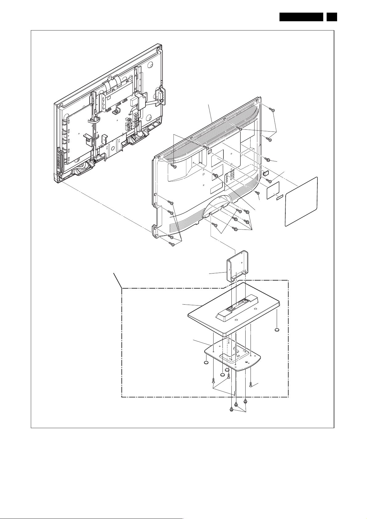
[4] Rear Cabinet
FUZ2.0U LA 19
Stand Assembly
[2] Stand Cover
(S-4)
(S-4)
[3] Stand Hinge
(S-4)
(S-6)
(S-4)
(S-5)
(S-6)
(S-1)
(S-4)
[1] Stand Base Plate
(S-3)
(S-3)
(S-2)
Fig. D1

20 FUZ2.0U LA
[9] Digital Main
Board Unit
[8] Shield Box
(S-13)
(S-11)
[10] Power Supply Board
(S-12)
(S-13)
(S-7)
(S-15)
(S-14)
(S-14)
[6] Side Jack
Board
(N-1)
(S-15)
(S-15)
[5] Jack Holder (A)
(S-7)
(S-8)
[7] Shield (T)
(S-10)
(S-9)
Fig. D2
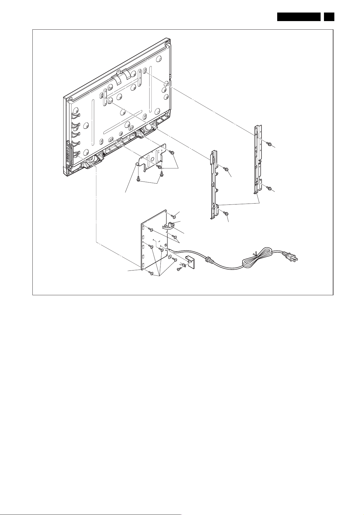
(S-19)
[14] Stand Holder
(S-18)
(S-16)
FUZ2.0U LA 21
(S-17)
(S-17)
(S-17)
[13] PCB Holder (L,R)
[11] Inverter Board
(S-16)
Desolder
(S-17)
[12] Junction-B Board
(S-16)
Fig. D3
22 FUZ2.0U LA
[21] Front Cabinet
[20] Speaker
(S-22)
[18] Function
Board
[20] Speaker
(S-23)
(S-23)
Desolder
[16] Junction-A
Board
(S-21)
[17] IR Sensor
Board
(S-23)
[19] Speaker
Holder (L,R)
[15] LCD Module Assembly
(S-23)
[19] Speaker
Holder (L,R)
(S-20)
Fig. D4
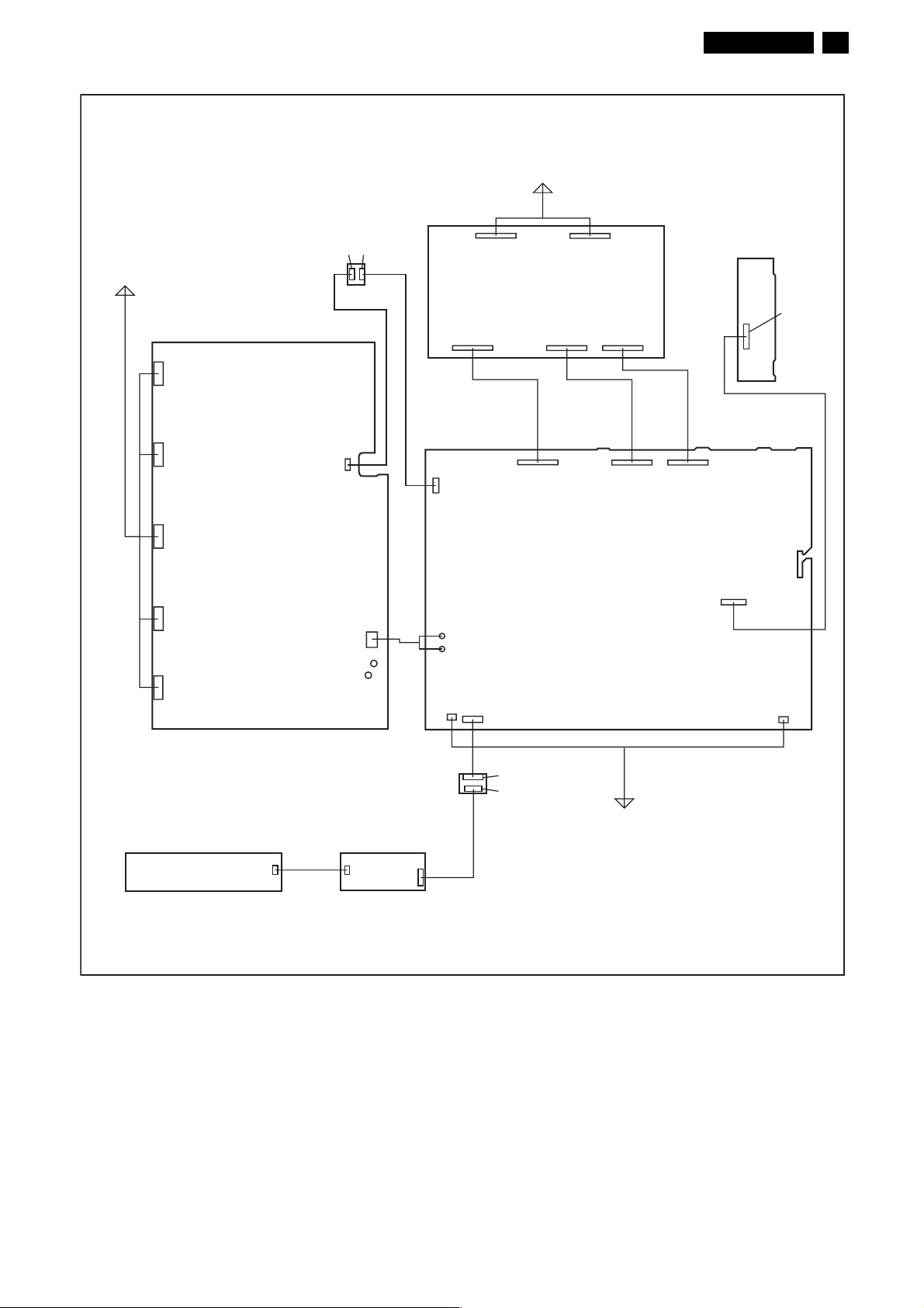
TV Cable Wiring Diagram
To LCD
Module
Assembly
Inverter Board
CN1050
CN1100
Junction-B
Board
CL1000A
FUZ2.0U LA 23
To LCD Module
Assembly
Digital Main
Board Unit
CN1000CL1000B
CN4501 CN4502
CN3601 CN3701
CN3704
Side Jack
Board
CN751
Power Supply
Board
CN301 CN302 CN303
CN501
CN1150
CN1200
CN1250
Function Board
CL102B
CN1901
AC CORD
Junction-A
Board
IR Sensor Board
CL101A
CL102A
CN601
CN802
CN102
CN101
CL101B
CN701
CN801
To Speaker
Fig. D5
24 FUZ2.0U LA
7. TROUBLESHOOTING
7.1 Power Supply Section
FLOW CHART NO.1
The power cannot be turned on.
Is the fuse (F1901) normal?
Ye s
Is normal state restored when once unplugged
power cord is plugged again several seconds?
Ye s
Is the AL +13V line voltage normal?
Ye s
Check each rectifying circuit of the secondary
circuit and service it if defective.
FLOW CHART NO.2
The fuse blows out.
Check the presence that the primary component
is leaking or shorted and service it if defective.
After servicing, replace the fuse.
FLOW CHART NO.3
When the output voltage fluctuates.
No
No
No
See FLOW CHART No.2 <The fuse blows out.>
Check if there is any leak or short-circuiting on the
primary circuit component, and service it if defective.
(C601, D1901, D1902, D1903, D1904, Q601, Q603,
T601)
Check the presence that the rectifying diode or circuit
is shorted in each rectifying circuit of secondary side,
and service it if defective.
Does the photocoupler circuit on the
secondary side operate normally?
Ye s
Check IC603, D603, D607 and their periphery,
and service it if defective.
FLOW CHART NO.4
When buzz sound can be heard in the vicinity of power circuit.
Check if there is any short-circuit on the rectifying diode and the circuit in each rectifying circuit of the secondary side,
and service it if defective. (IC637, D503, D632, D633, D636, D637, D638, D639, D640, D647, D669)
FLOW CHART NO.5
+40V is not output.
Is approximately 40V voltage supplied to the
cathode of D636?
Ye s
Check if there is any leak or short-circuit on
the loaded circuit, and service it if defective.
No
No
Check IC603, D631, Q631 and their periphery,
and service it if defective.
Check C639, D636 and their periphery circuit, and
service it defective.

FLOW CHART NO.6
AL+13V is not output.
FUZ2.0U LA 25
Is approximately 13V voltage supplied to the
cathode of D638?
Ye s
Check if there is any leak or short-circuit on
the loaded circuit, and service it if defective.
FLOW CHART NO.7
AL+3.3V is not output.
Is approximately 6.6V voltage supplied to the
cathode of D669?
Ye s
Check IC637, D654, D657 and their periphery circuit,
and service it if defective.
FLOW CHART NO.8
P-ON+5V is not output.
Is approximately 6.6V voltage supplied to the
collector of Q637?
Ye s
Is approximately 6V voltage supplied to the
base of Q637?
Ye s
Replace Q637.
No
No
No
No
Check C638, D638, D639 and their periphery circuit,
andservice it defective.
Check C654, D669 and their periphery circuit, and
service it if defective.
See FLOW CHART No.7
See FLOW CHART No.10
FLOW CHART NO.9
LCD+24.5V is not output.
Is approximately 36V voltage supplied to the
cathode of D636?
Ye s
Is approximately 36V voltage supplied to the
collector of Q632?
No
Is the voltage of base on Q632 lower than the
voltage of emitter on Q632 when turning the
power on?
Ye s
Replace Q632.
No
Ye s
No
Check C639, D636 and their periphery circuit, and
service it if defective.
Check D641, D652 and their periphery circuit, and
service it if defective.
Check Q634 and P-ON-H1 line, and
service it if defective.
26 FUZ2.0U LA
FLOW CHART NO.10
LCD+13V is not output.
Is approximately 15V voltage supplied to the
cathode of D633?
Ye s
Is approximately 14V voltage supplied to the
base of Q645?
Ye s
Replace Q645.
FLOW CHART NO.11
LCD-6.8V is not output.
Is approximately -9V voltage supplied to the
anode of D637?
Ye s
Is approximately -9V voltage supplied to the
base of Q646?
Ye s
Replace Q646.
No
No
No
No
Check C633, D633 and their periphery circuit, and
service it if defective.
See FLOW CHART No.9
Check C663, D637 and their periphery circuit, and
service it if defective.
See FLOW CHART No.9
FLOW CHART NO.12
P-ON+3.3V (LCD+3.3V) is not output.
Is approximately 5V voltage supplied to the
cathode of D632?
Ye s
Is approximately 4V voltage supplied to the
base of Q638?
Ye s
Replace Q638.
FLOW CHART NO.13
+3.0V is not output.
Is approximately 3V voltage supplied to the
cathode of D647?
Ye s
Check if there is any leak or short-circuit on
the loaded circuit, and service it if defective.
No
No
No
Check C634, D632 and their periphery circuit, and
service it if defective.
Check Q639, Q671 and their periphery circuit, and
service it if defective.
Check C664, D647 and their periphery circuit, and
service it if defective.
FLOW CHART NO.14
+3.0V(1) is not output.
FUZ2.0U LA 27
Is approximately 3V voltage supplied to the
cathode of D640?
Ye s
Check if there is any leak or short-circuit on
the loaded circuit, and service it if defective..
FLOW CHART NO.15
P-ON+9V is not output.
Is approximately 13V voltage supplied to the
collector of Q801?
Ye s
Is approximately 10V voltage supplied to the
base of Q801?
Ye s
Replace Q801.
FLOW CHART NO.16
The key operation is not functioning.
No
No
No
Check C642, D640 and their periphery circuit, and
service it if defective.
See FLOW CHART No.6
See FLOW CHART No.10
Are the contact point and installation state of the key
switches (SW108, SW109, SW110, SW111,
SW112, SW113, SW114) normal?
Ye s
When pressing each switches (SW108, SW109,
SW110, SW111, SW112, SW113, SW114) do the
voltage of Pin(1) on CN301 increase?
Ye s
Replace Digital Main Board Unit.
No
No
Re-install the switches (SW108, SW109, SW110,
SW111, SW112, SW113, SW114) correctly or
replace the poor switch.
Check the switches (SW108, SW109, SW110,
SW111, SW112, SW113, SW114) and their
periphery, and service it if defective.
28 FUZ2.0U LA
FLOW CHART NO.17
No operation is possible from the remote control unit.
Operation is possible from the remote control unit.
Is 3.3V voltage supplied to Pin(2) terminal of the
infrared remote control receiver (RCV101)?
Ye s
Is the "L" pulse sent out Pin(1) terminal of receiver
(RCV101) when the infrared remote control is
activated?
Ye s
Is the "L" pulse supplied to the Pin(4) of CN301?
Ye s
Replace Digital Main Board Unit.
No
No
No
7.2 Video Signal Section
FLOW CHART NO.18
Picture does not appear normally. (Video input/S-Video input/Y/Pb/Pr input)
Are the video signals outputted to the specific
terminal?
Are the video signals outputted to the
Pin(23) of CN302?
Are the luminance signals outputted to the
Pin(19) of CN302?
Are the chrominance signals outputted to the
Pin(21) of CN302?
Are the component video(Y/Pb/Pr) signals outputted
to the Pin(14, 16, 17) of CN302?
Ye s
No
No
No
No
Check AL+3.3V line and service it if defective.
Replace the infrared remote control receiver
(RCV101) or the remote control unit.
Check the line between Pin(1) terminal of receiver
(RCV101) and Pin(4) of CN301 , and service
it if defective.
Check the line between each pin of CN302 and input
terminal and service it if defective.
Check the video signal line and IC7001,
and service it if defective.
Check the luminance signal line and IC7001,
and service it if defective.
Check the chrominance signal line and IC7001,
and service it if defective.
Check the component video(Y/Pb/Pr) signal line
and IC7001, and service it if defective.
Replace Digital Main Board Unit or LCD Module
Assembly.
FLOW CHART NO.19
Picture does not appear normally. (Tuner input (Digital))
Are the DIF signals outputted to the Pin(20, 22) of CN303?
Ye s
Replace Digital Main Board Unit or LCD Module
Assembly.
FLOW CHART NO.20
Picture does not appear normally. (Tuner input(Analog))
Are the video signal outputted to Pin(11) of CN303?
Ye s
Replace Digital Main Board Unit or LCD Module
Assembly.
No
No
Check the line between Pin(20, 22) of CN303 and
Pin(20, 21) of TU1 and TU1(Tuner Unit),
and service it if defective.
Check the line between Pin(11) of CN303 and
Pin(4) of TU1 and TU1(Tuner Unit),
and service it if defective.
 Loading...